Voltage-Mode Universal Biquadratic Filter Using
Tunable OTA in 180nm Technology
Smaranika Sahoo1, Sruti Suvadarsini Singh2
1
M.Tech in VLSI & ES, School of Electronics Engineering, KIIT University, 2
Assistant Professor, School of Electronics Engineering, KIIT University, Bhubaneswar, India
Abstract: Conventional Operational Amplifiers (Op-Amps) limit their applications at high frequencies. Since output is a voltage, Op-Amps limit to frequencies up to few Megahertz. At those high frequencies, Operational Transconductance Amplifiers (OTAs) are being promising to replace Op-Amps as building blocks. OTAs are useful in realisation of active Gm-C filters. A Balanced OTA which is the simplest configuration of an Operational Transconductance Amplifier is chosen as a basic building block for the present work. The resulting OTA has improvement as compared to the basic balanced OTA in terms of better gain, CMRR and slew rate. Further, the improved circuit of balanced OTA is used to implement tunable OTA. The Tunable OTA designed in the present work has gain 55.48dB, Common Mode Rejection Ratio (CMRR) of 133.775dB, Slew rate of 45.67V/μs. A Bi-Quad Filter is implemented using Tunable OTA as an application example. A Low pass, High pass, Band pass, Band Reject and All pass filters are demonstrated by controlling the input control voltages. The circuits are implemented in gpdk180 in Cadence software.
Keywords - Operational Transconductance Amplifiers (OTAs), Common Mode Rejection Ratio (CMRR), gain, Balanced OTA, Tunable OTA
I. INTRODUCTION
Tunable OTA is a versatile building block for continuous time analog signal processing. Tuning of transconductance (gm) is an important requirement in many applications such as gm-C active filters, tunable grounded resistors, automatic gain control circuits, etc. Transconductance tuning is required not only to compensate for fabrication tolerances but also to achieve programmability of relevant parameters. Tuning in operational transconductance amplifier (OTA) is achieved by either varying transconductance as function of control voltage or bias current. With recent scaling in CMOS technologies use of voltage as control parameter for tuning is becoming increasingly difficult and thus for low voltage OTA applications, tuning is often achieved using bias current as it shows better linear range at low voltages.[1]
[image:2.612.174.418.552.710.2]Tunability provides flexibility to change the range of filters and also the gain in automatic gain controllers. The OTA is known as tunable OTA when the MOSFET using in it operating in saturation or triode regions. If we change the control voltage or the bias current, then the transconductance will be varied. Because of linearity restrictions, the circuits which use voltage as control parameter to change the OTA transconductance will have limited range of operation at low voltage. OTA transconductance can also be made vary by changing the bias current. [6][7]
The tunable OTA is modelled as three input and one output terminals device as shown in Figure 1.1. Where V+ and V- is the input
voltages applied at non-inverting terminal and inverting terminal respectively. Ibias is the bias current. The transconductance should
be linearly dependent on the bias current for linear filter application. The circuit is biased by a constant current source. The use of constant current source is to prevent the transistors from leaving strong inversion region and hence improves the linearity.
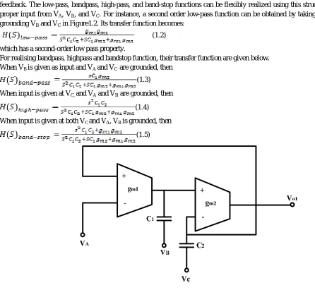
A. Second Order Bi-Quad Filter
Operational amplifiers can be used to realize a linear system with an arbitrary biquadratic transfer function. A biquad transfer function can be realized straightforwardly with a pair of integrators in series, each introducing a factor 1/s, with their outputs added to the input signal in a summer.
The parameters f0, Q and the band pass gain at the centre frequency are given in terms of the circuit parameters.[2]
The general second order (bi-quadratic)filter transfer function is given by,
(1.1)
Figure 1.2 gives a structure of second-order biquad filters based on the OTA integrators. Each structure contains a global negative feedback. The low-pass, bandpass, high-pass, and band-stop functions can be flexibly realized using this structure by selecting the proper input from VA, VB, and VC. For instance, a second order low-pass function can be obtained by taking VA as the input and
grounding VB and VC in Figure1.2. Its transfer function becomes:
(1.2)
which has a second-order low pass property.
For realising bandpass, highpass and bandstop function, their transfer function are given below. When VB is given as input and VA and VC are grounded, then
(1.3)
When input is given at VC, and VA and VB are grounded, then
(1.4)
When input is given at both VC and VA, VB is grounded, then
[image:3.612.41.487.264.675.2](1.5)
Figure 1.2 : Bi-Quad Filter using OTA
II. CIRCUITS AND OPERATION A. Balanced OTA circuit
[image:4.612.89.525.196.426.2]The circuit is called a symmetric or three current-mirror OTA uses self-biased loads. It has a larger trans-conductance, slew rate, and GBW. These specifications are made larger by increasing current mirror factor. The trans-conductance can be set by the tail current source, current mirror ratio, or size of the input transistors. The trans-conductance is usually the most important parameter, and it is fortunate that it can be determined by several parameters. Automatic tuning circuits sometimes vary the bias current in order to adjust the trans-conductance to the desired value. The phase margin is a measure of stability for the amplifier. This circuit is constructed from all the basic elements. The input stage is a differential pair. The sub-circuits composed of M1,3 and M2,4 are self-biased inverters. Transistors M3,5 M4,6 M7,8 and are simple current mirrors.[1][3]
Figure 2.1: Design of balanced OTA in cadence tool
When designing the symmetrical OTA, transistors M1 =M2, M3=M4, M5=M6, and M7=M8. This reduces the number of designable parameters to four transistor sizes and the tail current.[1]
Table 2.1: Transistor sizing of Balanced OTA
Transistors W/L (µm/ µm)
M1, M2 0.40/0.18
M3, M4 0.40/0.18
M5, M6 6/0.18
[image:4.612.74.538.530.716.2]M7, M8 0.70/0.18
Table 2.2: Input specification for balanced OTA
Technology Cadence gpdk180
Supply voltage 1.8 V
Input voltage in+ AC amplitude =500 mV
Magnitude = 1 mV
Input voltage in- AC amplitude = 1 mV
Magnitude = 1 mV
Frequency 1 KHz
DC current 10 µA
B. Tunable OTA circuit
Tunable OTA comprises of two stages of BOTA and a resistor connected in between the two stages. The first stage converts the differential input signal voltage into a signal current Io to flow into a resistor (Active-R). The voltage across the resistor is VR is
given by:
(2.1)
The schematic of Tunable OTA is shown in Figure 4 and the voltage drop across resistor is given by:
(2.2)
(2.3) The total current Iout is given by,
(2.4)
(2.5)
and (2.6)
(2.7)
[image:5.612.40.505.56.715.2]Where β is the transconductance parameter of Active-R transistors.[5]
Figure 2.2: Design of Tunable OTA in Cadence
Table 2.3: Transistor sizing of Tunable OTA
Transistors W/L(µm/ µm)
M1, M2,M11, M12 7.2/0.18
M3, M4, M13, M14 10.8/0.18
M5, M6, M15, M16 9.8/0.18
M7, M8, M17, M18 9.6/0.18
C. Bi-Quad Filter using TOTA
Figure 2.3: All pass filter using TOTA
III. SIMULATION RESULTS
Figure3.1. Amplified output of OTA at Cadence tool A. AC Analysis
Gain=32.9 dB UGB=344.40 MHz
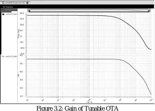
Figure 3.2: Gain of Tunable OTA
The gain of the tunable OTA is coming 55.48 dB with phase margin 209.32MHz.
The power dissipated at the output is coming 8.615mW. Slew rate is 45.67 . The worst case delay propagation through critical
[image:6.612.179.434.489.671.2]B. CMRR
Figure 3.3: CMRR of Tunable OTA
CMRR of this circuit can be calculated as
[image:7.612.94.484.275.716.2](3.1)
Figure 3.4:Low pass Response of TOTA
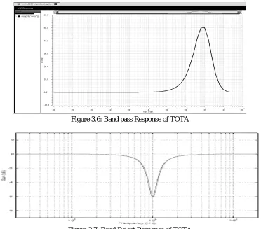
Figure 3.6: Band pass Response of TOTA
Figure 3.7: Band Reject Response of TOTA
IV. CONCLUSION
All designs are done in Cadence gpdk180. The balanced OTA has gain of 32.9 dB, Slew rate is 48.61 V/μS, CMRR is 123.91 dB,
120μW power dissipation. The advanced tunable OTA has gain of 55.48 dB, Slew Rate is 45.67 V/μS, CMRR is 133.775 dB and 8.615 mW power dissipation. In addition, the performance of both balanced and Tunable OTA is verified in the Simulation. A Bi-Quad Filter is implemented using Tunable OTA as an application example. A Low pass, High pass, Band pass, Band Reject and All pass filters are demonstrated by controlling the input control voltages.
REFERENCES
[1] Lucía Acosta, Mariano Jiménez, Ramón G. Carvajal, Antonio J. Lopez-Martin, ” Highly Linear Tunable CMOS -Low-Pass Filter” IEEE TRANSACTIONS ON CIRCUITS AND SYSTEMS—I: REGULAR PAPERS, VOL. 56, NO. 10, OCTOBER 2009.
[2] R. L. Geiger and E. Sanchez-Sinencio, “Active filter design using operational transconductance amplifiers: A tutorial,” IEEE Circuit and Device Magazine, vol. 1, pp. 20-32, Mar. 1985.
[3] F. A. P. Baruqui and A. Petraglia, “Linear tunable CMOS OTA with constant dynamic range using source-degenerated current mirrors,” IEEE Trans. Circuits and Systems II: Express Briefs, vol. 53, no. 9, pp. 797-801, Sep. 2006.
[4] T. Lo and C. Hung, “A 1-V 50-MHz pseudo differential OTA with compensation of the mobility reduction,” IEEE Trans. Circuits and Systems II: Express Briefs, vol. 54, no. 12, pp. 1047-1051, Dec. 2007.
[5] T. Lin, C. Wu, and M. Tsai, “A 0.8-V 0.25-mW current-mirror OTA with 160- MHz GBW in 0.18-um CMOS,” IEEE Trans. Circuits and Systems II: ExpressBriefs, vol. 54, no. 2, pp. 131-135, Feb. 2007.
[6] F. A. P. Baruqui and A. Petraglia, “Linear tunable CMOS OTA with constant dynamic range using source-degenerated current mirrors,” IEEE Trans. Circuits and Systems II: Express Briefs, vol. 53, no. 9, pp. 797-801, Sep. 2006.nics, vol. 88, pp. 1093–1101, 2001
[7] H.–P. Chen, S.– S.Shen, and J.–P. Wang, ―Electronically tunable versatile voltage-mode universal filter, International Journal of Electronics and Communications, vol.62, pp. 316-319, 2008