JEEECCS, Volume 1, Issue 1, pages 21-26, 2015
System for Generating Very High Precision
Sinusoidal Signals
Arcan Alexandru-Marian
Department of Networks and Telecommunication Software, ECC Faculty, University of Pitesti
Pitesti, Romania
Abstract – The article presents the realization of a System For Generating Very High Precision Sinusoidal Signals using a DDS (Direct Digital Synthesizer), a programmable digital circuit able to generate signals with a very small error, high fidelity and high stability.
Keywords: DDS, high fidelity, very small error, high stability.
I. INTRODUCTION
DDS are programmable digital circuits capable of generating very high fidelity signals. Although their working principle is known for many years they have not played an important role in generating broadband frequencies signals because they were limited by the D / A converters (Digital - Analog). Moreover, they consume power quite large and had considerable size, being first used in the military domain. Modern DDS are extremely small, on the order of mW power consumption and are commonly used in applications such as modulators, demodulators, various communications systems, radio software define, radar, etc. due to their performance.[1]
Chapter 2 presents the operating principle of a DDS starting from its internal scheme and explaining the main steps with which this little circuit can generate very high precision signals. In addition in this chapter are presented the main parameters of these circuits .
Chapter 3 presents the hardware design of the system starting from its block diagram detailing the main issues in choosing components
Chapter 4 presents the software design of the system which includes the main program flowchart and communication protocol restrictions that must be respected to communicate with the circuit
Chapter 5 presents practical results where there can be observed system functionality and performances at different work frequencies.
II. WORKING PRINCIPLE OF DDS
DDS is a programmable circuit which has many advantages such as reduced size and power consumption measured in mW, is easy to configure and make quick jumps between frequencies. Moreover it can be programmed to generate both
sinusoidal, triangular or rectangular signals whose maximum frequency and resolution depends on a reference oscillator that is the only external component that DDS needs after it was programmed. The calculation formula for the resolution is in the equation (1) :
28
2
MCLK
F
RESOLUTION
(1)Four examples of resolution of the output signal depending on the frequency of the reference oscillator are presented in the following table: [2]
Table 1. DDS resolutions
FMCLK RESOLUTION
1MHz 0.004Hz
10MHz 0.04Hz
25MHz 0.1Hz
40MHz 0.16Hz
It is seen form the table that we can not have at the same time a good resolution and a high working frequency, so that a compromise will be made in this regard depending on the application where DDS is used
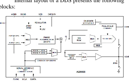
Internal layout of a DDS presents the following blocks:
Figure 1. Intern DDS layout
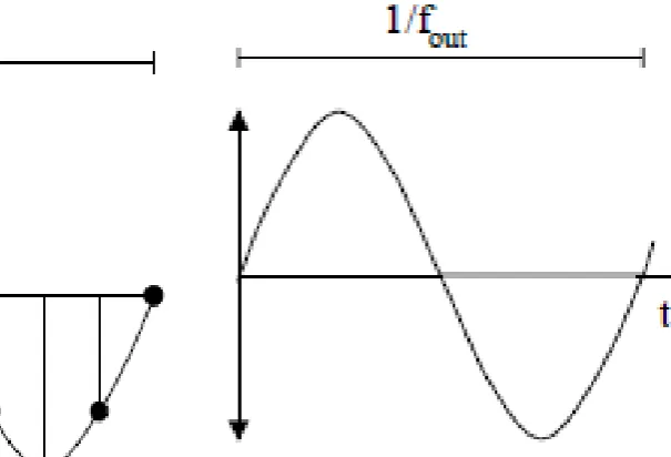
frequency and phase registers. The information from the 2 frequency registers reaches a 28-bit phase accumulator. Its output is summed with the information from the 2 phase registers reaching at the exit of the adder samples of different phases resembling a sawtooth signal as shown as shown in figure 2. :[2]
Figure 2. Signal at ROM memory input
This signal reaches the input of a ROM memory, which functions as a phase – amplitude converter generating at its output one sample with amplitude corresponding to the input signal phase. This samples are the exactly the samples from the signal you want at the DDS output as seen in figure 3. :
Figure 3. Signal at ROM memory output
This signal then enters in a digital – analog converter that convert the discrete input signal into a continuous one as shown in figure 4.:
Figure 4. Signal at D/A converter output
It can be observed that the sinusoid obtained at the output of RAM memory is not clean, this is being formed through integrating some discrete signals, thus it being a step signal. If we visualize the spectral diagram of the signal we would observe the apparition of many more spectral components with a superior frequency than desired. In order to eliminate these frequencies there will be a low-pass filtering, inside the DDS, which will eliminate the components with a higher frequency than the useful signal, thus it is obtained the following signal:
Figure 5. Signal at DDS output
III. HARDWARE DESIGN
The block diagram of system is submitt in figure 6.:
Figure 6. System block diagram
The principal component of the system is DDS, the circuit who was submitted previous. To be working this requires a reference oscillator to provide it a stable time base. In order to the DDS it must be programmed, appointment what is done with a microprocessor. By appointment mode of work is set of circuit and parameter of output signal
In addition to change easier the frequency of the output signal the processor manage two more keys wich are designed to increase or decrease the output signal frequency with a particular step set by program depending of the application where the generator of signal is used.
Because DDS can generate at output signals with a maxim 650 mV amplitude it was added an operational amplifier on the output of system which is designed to lead the signal amplitude to a maxim 10V.
IV. SOFTWARE DESIGN
As a programmable circuit DDS must be controlled by a microprocessor. Because it was meant to provide a system with small dimensions and low cost has been opted for a processor from PIC12 family, a small processor with low consume and low cost that has SPI interface, this it's necessary because DDS programming is done using this protocol.
SPI protocol is a serial protocol, synchronous, which uses only 3-wire to communicate. However DDS impose certain restrictions on the SPI communication, as seen in Figure7.:[2]
Figure 7 SPI communication restrictions
It is noticed that somewhere in these restrictions include the minimum timings of signals that are given by the manufacturer in datasheet, active landing of Fsync which is 0 logic and FCLK pulse signals for reading data meaning falling edge. Considering these can be configured SPI interface for the processor to communicate with DDS.
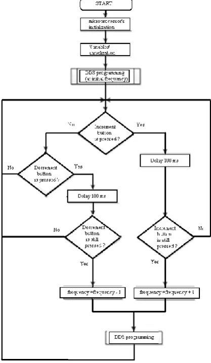
The main program flowchart is presented in the figure 8.:
Figure 8. Main program flowchart
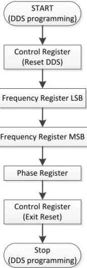
At effective programming DDS is programmed in just 5 steps presented in following flowchart:[3]
Control Register (Reset DDS)
Frequency Register LSB
Frequency Register MSB
Phase Register
Control Register (Exit Reset)
START (DDS programming)
Stop (DDS programming)
Figure 9. DDS programming flowchart
It noted that through the control word does not only transmit information about the reset, it is only compulsory condition to be fulfilled. With this control word the user can choose how they make writing in the registry frequency and phase, sleep functions of DDS's and of output signal type . If that change any of the parameters of frequency or phase should be followed again across organizational, even if, for example, we want to modify only the information in the phase register must first relaying information from the frequency register by which we can make the desired changes. [3]
We must not forget that the buttons mentioned above with which we can increase or decrease the frequency of the output signal are mechanical buttons and bouncing effect can occur, so should be performed debouncing software to eliminate any inconvenience.
V. PRACTICAL RESULTS
Bearing in mind the above details was done the practically installation of generator of very high precision signals.
After the practical realization system has been tested to generate sinusoidal signals in the range 10-100 Hz. It can generate lower frequency but I have no disposed the necessary equipment for the measurements. After testing were performed following oscilloscope screenshots:
Figure 10. Signal obtained for 10 Hz
Figure 11. Signal obtained for 30 Hz
Figure 13. Signal obtained for 100 Hz
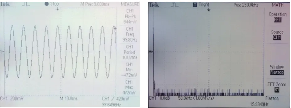
It is noticed in the 4 figures are obtained primarily as perfect sinusoids as their amplitude is constant regardless of frequency signal. In addition it can be seen the error of the circuit, error in case we wanted to get 10 Hz was 0.4% yielding 9.96 Hz. This error is quite high because the circuit error between 0 and 0.5%, so we have a maximum error. Still fault circuit is not constant while varying it. So for a desired signal of 30 Hz to obtain a frequency of 29.94 Hz that is an error of 0.2%, or a desired signal 90 Hz 89.93 Hz yield of 0.077% that is an error, an error just below 0.1%. Last measurement was performed for 100 Hz frequency which achieved a 0.2% error .We can see that the error decreases or after a certain law but simply be in the range 0 - 0.5%.
To convince us of DDS capabilities there were performed a Fourier transform using the oscilloscope case to notice the the spectrum of the signal generated by the track and see if sinusoid generated is clean or if there appear other spectral components besides the fundamental . Oscilloscope screen captures are shown in the following figure:
Figure 14. FFT on a 50 Hz band
Figure 15. FFT on a 500 KHz band
Both measurements are performed at the same frequency of 20 Hz only thing that differ from each other that is the scale,the scale of the Figure 11 having 5 Hz / division, while in Figure 12 with 50 kHz / division. In Figure 11 we can observe spectral component positioning exactly on 20 Hz, and the figure 12 is observed as a spectrum of 500 KHz not have other spectral components. Because the spectrum we have only 20 Hz fundamental frequency harmonics without any addition it means that we have a pure sinusoid.
No measurements were performed on a larger spectrum as the noise grew very comparable to the signal. This noise can be reduced significantly if a battery to power the circuit.
VI. CONCLUSIONS
We were able to achieve one system with low consumption and low cost which was easy to interpret and to configure , which can generate not only sinusoid signal but rectangular or triangular too with an frequent up to 10 MHz , with an maximum error of 0,5% and an resolution 0.04 Hz . Depending on the application where it s used you can opt for an big speed of work and an high rate of error or you can opt for a low speed of work at an low frequent of work , which can be changed simply by changing the reference oscillator. In addition the system is easy to manipulate using 2 keys to increase or decrease the output signal frequency of the system
The system can be upgraded as needed, such as you can add a key to change the shape of the output signal, which was not done because it wanted to keep simplicity and low cost of the project, and this needs a bigger process with more pins.
ACKNOWLEDGEMENTS
Thanks to Prof. Iana Vasile Gabriel who guided me in the diploma project and sacrificed some of his time whenever I needed guidance. I would like to thank the research center Mira Telecom where Prof. Iana Gabriel offered me possibility to do the diploma project using latest equipment.
REFERENCES
[1] PhD degree of Jouko Vankka – Direct Digital Synthesizers: Theory, Design and Applications
[2] Analog Devices – datasheet Programable Waveform Generator AD9833