International Journal of Science Engineering and Advance
Technology, IJSEAT, Vol. 5, Issue 4
ISSN 2321-6905
April -2017
A New Modular Multilevel Inverter Topology of Reduced Components
P Venkateswara Rao1, S Hema Supriya Reddy2
PG Student, Department of EEE, Pydah College of Engg, Kakinada, India.1 Asst.Professor, Department of EEE, Pydah College of Engg, Kakinada, India.2
Abstract— Harmonic content of the yield voltage waveform diminishes as the quantity of yield voltage level increments. The primary focal points are lower Total Harmonic Distortion (THD), less weight on the power switches and higher proficiency. Be that as it may, increment in the gadget number because of expanded voltage levels makes the control strategy complex and subsequently costly. This venture displays a nine level inverter with lessened DC sources which is equipped for acquiring all added substance and subtractive mixes of information DC levels. This topology requires less power changes contrasted with regular multilevel inverter and less entryway drives. The proposed topology is exhibited through a nine-level inverter with a proper balance plot and definite reproduction has been done in MATLAB/Simulink. A correlation is made between proposed topology and the customary multilevel topology on the premise of gadget include, number of levels the yield voltage and THD.
Index Terms—Classical topologies, multilevel inverter (MLI), pulsewidth modulation (PWM), reduced component count, total harmonic distortion (THD).
I. INTRODUCTION
Over the most recent couple of decades, multilevel voltage-source inverters have risen as a practical answer for high-control dc-to-air conditioning change applications [2]. A multilevel inverter (MLI) is a linkage structure of different info dc levels (gotten from dc sources as well as capacitors) and power semiconductor gadgets to blend a staircase waveform. Voltage stresses experienced by the power switches are lower when contrasted with the general working voltage level [3]. Also, the multilevel waveform has a superior consonant profile when contrasted with a two-level waveform acquired from regular inverters. Different focal points of MLIs are decreased dv/dt weight on the heap and plausibility of blame tolerant operation [4]. Specialists are additionally investigating roads to utilize MLIs for low-control applications [5].The nature of the multilevel waveform is upgraded by expanding the quantity of levels. Nonetheless, it incidentally prompts countless semiconductor gadgets and going with door driver circuits. This expands framework unpredictability and cost and has a
tendency to diminish the framework unwavering quality and proficiency. For a high-determination waveform, in this manner, useful contemplations require decrease in the quantity of switches and entryway driver circuits [6].The topologies which have been broadly examined and are industrially accessible for multilevel voltage yield are impartial point clasped (NPC), fell H-connect (CHB), and flying capacitor (FC) converters [2], [4], [5]–[7]. Be that as it may, there is a critical increment in the quantity of energy switches, the quantity of switches leading all the while, and the general cost of the framework with the expansion in the quantity of yield levels. Specialists, hence, keep on focusing on decreasing the segment check in multilevel topologies through different methodologies. These methodologies can be characterized into three classifications: topological changes [9]–[12], utilization of deviated sources [14]–
[16], and mix of topological changes and unbalanced source setups [17]–[19]. In this venture, another topology is proposed in which interchange dc sources are connected in inverse polarities by means of energy switches. This approach altogether reduces the quantity of energy switches required when contrasted with the traditional topologies. In addition, for symmetric information dc sources, the proposed topology demonstrates closeness with the CHB topology in two ways: 1) It needs different detached info dc voltages; and 2) input dc voltage levels can be joined into every single added substance esteem. In this manner, the topology can be utilized as an utility interface for sustainable power source frameworks where a substantial number of disengaged dc sources are accessible [3], [8], [10]. It can likewise be utilized as a part of medium-voltage drive applications where a stage moving transformer with different auxiliary windings is for the most part utilized (chiefly for the diminishment of line current bending), in this way giving separated dc sources [7]. The proposed topology may likewise be suitable for battery-controlled applications, (for example, electric vehicles and submarine drive).
II. PROPOSED MULTILEVEL TOPOLOGY
the help of a solitary stage five-level inverter. Expressions for yield voltage, source streams, voltage stresses, and so forth., are moreover introduced.
A. Summed up Structure
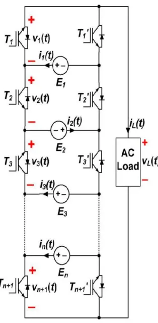
The summed up single-stage structure of the proposed topology is appeared in Fig. 1. It has n number of secluded info dc sources. The linkage structure is with the end goal that the higher potential terminal of the former source is associated with the lower potential terminal of the succeeding source and the other way around through power switches. Input sources are assigned as Ej (where j = 1 to n). Source current from each source is assigned as ij(t).
Fig. 1. Generalized single-phase structure of the proposed topology.
Control switches can be actualized utilizing a transistor gadget [e.g., MOSFET and protected entryway bipolar transistor (IGBT)] with an antiparallel diode. In Fig. 1, control switches are
represented with IGBTs with antiparallel diodes, and integral sets are assigned as (Tj, T_j) (where j = 1 to n + 1). Different nodal voltages are shown as vj(t) (where j = 1 to n + 1). Stack voltage and load current are assigned as vL(t) and iL(t), separately.
B. Working Principle
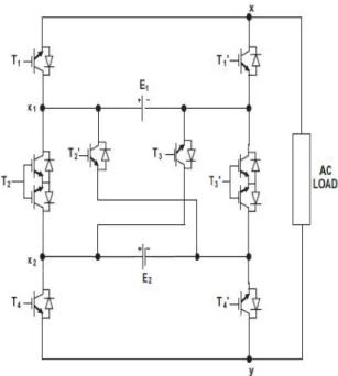
The working standard of the proposed topology is portrayed with the assistance of a solitary stage inverter with two information dc sources E1 and E2, as appeared in Fig. 2. It has three sets of dynamic switches (Tj, T_ j) (j = 1, 2, 3). Since the components of these sets are reciprocal, there are eight legitimate working modes. These modes are appeared in Fig. 3 and are abridged in Table I alongside nodal voltages and source streams. With the utilization of the working modes appeared in Fig. 3, the heap is provided with five levels, viz., }Vdc, }2Vdc, and zero for E1 = E2 = Vdc. With such a symmetric source setup, modes 3 and 4 wind up plainly repetitive for yield level +Vdc, while modes 6 and 7 end up noticeably excess for yield level−Vdc. It is imperative to note here that,
for all positive voltage levels and one "zero" level (modes 1, 3, 4, and 5), switch T_ 2 dependably directs, while for all negative voltage levels and another "zero" level (modes 2, 6, 7, and 8), switch T2 dependably leads. In this way, it is conceivable to work these two switches at the essential recurrence to get five yield levels. To do as such, modes 1, 3 (or 4), and 5 should be utilized for the union of positive levels (counting a "zero" level), and modes 2, 6 (or 7), and 8 should be utilized for the combination of negative voltage levels (counting a "zero" level).
Fig. 2. Single-phase inverter based on the proposed topology with two input sources.
this variety, both equipment based arrangements (e.g., utilizing separate dc–dc converters [8]) and control-calculation based arrangements (e.g., battery adjusting technique [19]) can be executed.
In the praposed topology has eight changes and to get any coveted voltage level, three changes should be ON. There are four sets of complimentary switches. Subsequently, three changes (to stay ON) can be browsed four conceivable outcomes in 4C3 (= 4) ways and each switch has two potential outcomes (either ON or OFF). In this manner, add up to number of states feasible for the topology is 24 = 16. In this single stage arrangement, the AC load is sustained by nine levels (E1 + E2), (E1), (E1 - E2), (E2), (0), (-E2), (E2 - E1), (- E1) and - (E1 + E2). It is additionally imperative to specify that any unbalance in information DC source extents would not bring about a multilevel waveform with equivalent voltage steps. All the conceivable states, voltage levels and switch positions are outlined in Table, where excess states are assigned as (1, 1‟), (2, 2‟),(5, 5‟, 5", 5‟"), (6, 6‟) and (7, 7‟). Excess can be utilized for ideal exchanging of energy semiconductor switches.
Fig. 3. Single-phase inverter based on the proposed topology with two input sources and eight switch network.
III. Control switch arrangements:
The proposed inverter can be acknowledged with self commutating power switches like MOSFET‟s and IGBT‟s.It is additionally essential to note that the switches at positions T2 and T‟3 are fundamentally
required to be „fully directional switches‟ generally
their undesirable exchanging will occur. In this manner, at both positions T2 and T‟3, completely directional switches having the capacity of blocking voltages in both bearings are to be utilized. A typical
producer mix is having low ON state drop however requires just a single door driver circuit. This switch arrangement has been decided for switches T2 and T‟3 of the proposed multilevel structure with two DC sources as appeared in Fig3.
IV. Exchanging SCHEME
High-exchanging recurrence balance strategies like multicarrier PWM and space vector regulation methods have been utilized for MLI adjustment control [22], [23]. On the
other hand, dynamic symphonious end, particular consonant
end, and central recurrence technique are considered as low-exchanging recurrence strategies [24]–[26]. The proposed topology can be regulated with any of these strategies with reasonable adjustment. In the present work, the multicarrier PWM plan is utilized. In a multicarrier PWM plot, bearer signs are contrasted and the reference flag, and the beats acquired are utilized for exchanging of gadgets comparing to individual voltage levels. In the proposed topology, one switch may contribute for blend of more than one level at yield terminals. In addition, as specified in Section II-B, appropriate use of six modes (viz., modes 1, 2, 3, 5, 6, and 8) will prompt central exchanging of T2 and T_
Fig. 4. (a) Reference and carrier waveforms for the proposed scheme for a Nine-level output.
IV.SIMULINK MODELLING
The component requirements of various topologies for a
three-phase configuration are given in [1] in terms of the number of voltage levels (N) in phase voltage. It can be inferred from the table that the number of components in the proposed structure is lower than those in other topologies, particularly for higher number of voltage levels. For example, implementing a nine-level inverter will entail component counts of 272, 188, and 108 for the NPC, FC, and CHB topologies, respectively, but only 72 in the proposed topology. It can also be observed from [1] that the proposed topology requires significantly lesser number of power switches than the classical topologies.
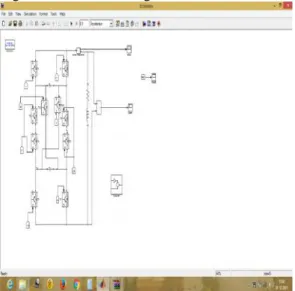
Fig5a:5-level inverter simulink diagram
Fig5b:Control block diagram
Fig6a:9-level inverter simulink diagram
Fig6b:Control block diagram for 9-level inverter
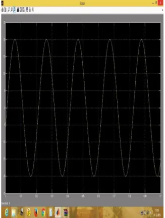
V.SIMULATION RESULTS
7(b) Harmonic spectrum of the load current
Fig. 8. Simulation results. (a) Five-level voltage output.
8(b) Harmonic spectrum of the load voltage
Simulation results.9 (a) Load current waveform
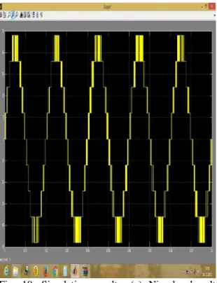
Fig. 10. Simulation results. (a) Nine-level voltage output.
10(b) Harmonic spectrum of the load voltage
VI. CONCLUSION
As MLIs are gaining interest, efforts are being directed toward reducing the device count for increased number of output levels. A novel topology for MLIs has been proposed in this project to reduce the device count. The working principle of the proposed topology has been explained, and mathematical formulations corresponding to output voltage, source currents, voltage stresses on switches, and power losses have
been developed. Simulation studies performed on a five-level inverter based on the proposed structure have been simulated and a nine level inverter also praposed .By the simulation observation the total harmonic distortion was reduced in nine level when compared to the five level inverter output. Comparison of the proposed topology with conventional topologies reveals that the proposed topology significantly reduces the number of power switches and associated gate driver circuits. Analytical comparisons on the basis of losses and switch cost indicate that the proposed topology is highly competitive. The proposed topology can be effectively employed for applications where isolated dc sources are available. The advantage of the reduction in the device count, however, imposes two limitations: 1) requirement of isolated dc sources as is the case with the CHB topology and 2) curtailed modularity and fault-tolerant capabilities as compared to the CHB topology.
REFERENCES
[1] A Novel Multilevel Inverter Based on Switched DC Sources Krishna Kumar Gupta and Shailendra Jain, Senior Member, IEEE
[2] S. Kouro, M. Malinowski, K. Gopakumar, J. Pou, L. Franquelo, B. Wu, J. Rodriguez, M. Perez, and J.
Leon, “Recent advances and industrial applications of
multilevel converters,” IEEE Trans. Ind. Electron.,
vol. 57, no. 8, pp. 2553–2580, Aug. 2010.
[3] G. Buticchi, E. Lorenzani, and G. Franceschini, “A
five-level single-phase grid-connected converter for
renewable distributed systems,” IEEE Trans.Ind. Electron., vol. 60, no. 3, pp. 906–918, Mar. 2013.
[4] J. Rodriguez, J.-S. Lai, and F. ZhengPeng,
“Multilevel inverters: A surveyof topologies, controls,
applications,”IEEE Trans. Ind. Electron., vol. 49, no.
4, pp. 724–738, Aug. 2002.
[5] S. De, D. Banerjee, K. Siva Kumar, K. Gopakumar, R. Ramchand, and C. Patel, “Multilevel
inverters for low-power application,” IET Power Electronics, vol. 4, no. 4, pp. 384–392, Apr. 2011.
[6] J. Rodriguez, S. Bernet, B. Wu, J. O. Pontt, and S.
Kouro, “Multilevel voltage-source-converter topologies for industrial medium-voltage drives,” IEEE Trans. Ind. Electron., vol. 54, no. 6, pp. 2930–
2945, Dec. 2007.
[7] L. M. Tolbert and F. Z. Peng, “Multilevel
converters as a utility interface for renewable energy
systems,” inProc. IEEE Power Eng. Soc. Summer Meeting, 2000, vol. 2, pp. 1271–1274.
[8] J. Ebrahimi, E. Babaei, and G. B. Gharehpetian, “A
new multilevel converter topology with reduced
Trans. Ind. Electron., vol. 59, no. 2, pp. 655–667, Feb. 2012.
[9] Y. Hinago and H. Koizumi, “A switched-capacitor inverter using series/ parallel conversion with
inductive load,” IEEE Trans. Ind. Electron., vol. 59,
no. 2, pp. 878–887, Feb. 2012.
[10] S.-J. Park, F.-S. Kang, M. H. Lee, and C.-U. Kim,
“A new single-phase five-level PWM inverter employing a deadbeat control scheme,” IEEE Trans. Power Electron., vol. 18, no. 3, pp. 831–843, May 2003.
[11] G.-J. Su, “Multilevel DC-link inverter,” IEEE Trans. Ind. Appl., vol. 41, no. 3, pp. 848–854, May/Jun. 2005.
[12] E. Najafi and A. H. M. Yatim, “Design and
implementation of a new multilevel inverter
topology,”IEEE Trans. Ind. Electron., vol. 59, no. 11,
pp. 4148–4154, Nov. 2012.
[13] J. Pereda and J. Dixon, “High-frequency link: A solution for using only one DC source in asymmetric cascaded multilevel inverters,” IEEE Trans. Ind. Electron., vol. 58, no. 9, pp. 3884–3892, Sep. 2011.
[14] T. A. Lipo and M. D. Manjrekar, “Hybrid
topology for multilevel power conversion,” U.S.
Patent 6 005 788, Dec. 21, 1999.
[15] X. Kou, K. A. Corzine, and Y. L. Familiant, “Full
binary combination schema for floating voltage source
multilevel inverters,” IEEE Trans.Power Electron.,
vol. 17, no. 6, pp. 891–897, Nov. 2002.
[16] Y. Ounejjar, K. Al-Haddad, and L. A. Dessaint,
“A novelsix-band hysteresis control for the packed U cells seven-level converter: Experimental validation,” IEEE Trans. Ind. Electron., vol. 59, no. 10, pp. 3808–
3816, Oct. 2012.
[17] C. A. Silva, L. A. Cordova, P. Lezana, and L.
Empringham, “Implementationand control of a hybrid multilevel converter with floating DC links for current
waveform improvement,” IEEE Trans. Ind. Electron.,
vol. 58, no. 6, pp. 2304–2312, Jun. 2011.
[18] K. K. Gupta and S. Jain, “Topology for multilevel
inverters to attain maximum number of levels from
given DC sources,”IET Power Electron., vol. 5, no. 4,
pp. 435–446, Apr. 2012.
[19] C.-M. Young, N.-Y. Chu, L.-R. Chen, Y.-C. Hsiao, and C.-Z. Li, “A single-phase multilevel
inverter with battery balancing,”IEEE Trans. Ind. Electron., vol. 60, no. 5, pp. 1972–1978, May 2013.
Authors:
P Venkateswara Rao pursuing M.TECH in Pydah College of Engg. ,Kakinada. His interested areas are power systems and power electronics.
S Hema Supriya Reddy currently