University of Dublin
Trinity College
Doctoral Thesis
Characterization, Simulation and
Optimization of Surface Etched Slotted
Tunable Laser Diodes
Author:
Michael
Wallace
Supervisor:
Prof. John
Donegan
A thesis submitted in fulfilment of the requirements
for the degree of Doctor of Philosophy
in the
Photonics Group
School of Physics
Declaration of Authorship
I, Michael Wallace, declare that this thesis titled, “Characterization, Simulation and
Optimization of Surface Etched Slotted Tunable Laser Diodes” and the work presented
in it are my own. I confirm that:
• This thesis has not been submitted as an exercise for a degree at this or any other university and it is entirely my own work.
• I agree to deposit this thesis in the University’s open access institutional repos-itory or allow the library to do so on my behalf, subject to Irish Copyright
Legislation and Trinity College Library conditions of use and acknowledgement.
• Where I have consulted the published work of others, this is always clearly
attributed.
• Where I have quoted from the work of others, the source is always given. With the exception of such quotations, this thesis is entirely my own work.
• I have acknowledged all main sources of help.
• Where the thesis is based on work done by myself jointly with others, I have made clear exactly what was done by others and what I have contributed myself.
Signed:
v
Summary
The past decades have seen near exponential growth in internet traffic. To meet
this growth, optical communication networks continue to branch deeper into network
architectures, replacing electrical based communication. In order to reduce
deploy-ment costs of such expansive networks, low-cost optical components integrated at
ever-increasing densities are needed. Tunable semiconductor laser diodes represent
an indispensable optical component in such networks, with significant research being
undertaken to reduce their cost and complexity. Such laser diodes are sensitive to thermal fluctuations and with increasing component density this thermal behaviour
becomes an important factor.
Previous research in the Trinity College Dublin semiconductor photonics group
has yielded a low-cost laser diode design based on surface etched slotted gratings. In
contrast to conventional low-order buried grating structures — used in distributed
feedback and distributed Bragg reflector lasers — slotted grating structures can be
fabricated without the need for re-growth or high resolution e-beam lithography.
This slotted design has previously been implemented in the form of tunable laser
arrays capable of covering the C-band with low linewidth and high SMSR. Further-more, widely tunable lasers based on the vernier effect have also been demonstrated
achieving > 50 nm tuning range. The research presented in this thesis builds upon the aforementioned work through experimental characterization, numerical simulation
and optimization of these slotted laser diodes.
Firstly, the tuning behaviour of multi-section single mode slotted laser diodes is
experimentally characterized in detail. This experimental characterisation yields a
more rigorous tuning scheme for the various laser sections, replacing the previous
ad hoc approach of avoiding mode hops. This tuning method is adopted to actively
athermalize the laser relative to changing ambient temperatures. Continuously tuned athermal operation is demonstrated from 8◦C to 47◦C with a wavelength stability of
±0.04 nm/±5 GHz and a minimum SMSR of 37.5 dB. Utilizing dis-continuous tun-ing, extended athermal operation is also demonstrated from 10◦C up to 85◦C, with
analytic predictive model for laser tuning is also developed utilizing surface
tempera-ture profile data measured via the CCD thermo-reflectance (CCD-TR) method. The
model proves capable of predicting tuning maps matching experimental results to a
high degree of accuracy.
A thermo-optic numerical model is subsequently developed (implemented using free and open source software), in order to accurately simulate a wide range of laser
dy-namics. This model utilizes the two-dimensional scattering matrix method (2D-SMM)
to model the slotted gratings, the time-domain transfer matrix method (TD-TMM) to
simulate the laser dynamics and the 3-D FEM solver FEniCS, to simulate the on-chip
temperature distribution. The model is compared to a range of experimental
measure-ments, including laser threshold, slope efficiency, linewidth, wavelength tuning maps
and CCD-TR measured temperature, and shows good agreement. The model is also
used to explain in detail the tuning dynamics of both single mode lasers and widely
tunable Vernier lasers. Moreover, the performance experimentally observed in widely tunable Vernier lasers is investigated through simulation. The relatively high tuning
current required for such lasers is attributed to the increasing carrier density in the
mirror sections. This high carrier density is also identified as likely being detrimental
to the linewidth and SMSR performance of such lasers.
Finally, a genetic algorithm is developed in order to optimize single mode
slot-ted laser diodes, with a view to improving efficiency and temperature stability. The
genetic algorithm incorporates the aforementioned 2D-SMM and TD-TMM to
ac-curately guide the optimization process toward ideal solutions. Using the genetic
algorithm, the previous iteration of laser array designs are re-optimized, yielding
de-signs with significantly improved output power and stability at elevated temperatures. Furthermore, the genetic algorithm is applied to optimize a laser for low linewidth
operation and a laser for direct modulation. The low linewidth design is theoretically
capable of achieving a linewidth of≤ 120 kHz; compatible with advanced modulation
formats such as 16PSK and 16QAM. A directly modulated laser design achieves a
theoretical performance of a −3 dB bandwidth of 30 GHz at 87.5 mA and clear
vii
Acknowledgements
I would like to express my sincere gratitude to my supervisor Professor John Donegan,
for giving me the opportunity to undertake this research. Over the past four years,
Professor Donegan’s supervision has made this work possible and I thank him for all
the invaluable advice, ideas, feedback, guidance and moral support, which were always
readily available. This supervision was also complemented with a freedom to pursue my own research interests and put my own mark on the research — an opportunity
which not all post graduate students are so lucky to be afforded with. Suffice it to
say, the past four years have been an incredible learning experience for me, and I
thank Professor Donegan wholeheartedly for this. Of course, this research would not
have been possible without the funding provided by CONNECT, Science foundation
Ireland and AMBER and I express my thanks for this.
I would also like to thank all the collaborating researchers who helped on this
project. I would like to thank Prof. David McCloskey for all his work on the
CCD-TR measurements. These measurements were also made possible by Simon Corbett, whose assistance is greatly appreciated. I would like to thank Rudi O’ Reilly Meehan
for his help with the laser athermalization experiments and Ryan Enright for his
insights on this topic.
I would like to thank both Marta Nawrocka and Azat Abdullaev for introducing
me to the experimental aspects of laser diodes and teaching me how to use the lab
equipment. I thank Gaurav Jain, Robert McKenna and Kevin Brazel for their help
with characterization. Furthermore, I would like to thank Jules Braddell for managing
device fabrication runs and teaching me about said fabrication. I would like to thank
Frank Bello for the many informative discussions on device modelling. I would also
like to thank the photonics group and the school of Physics as a whole for all their help over the years.
Though not directly involved in the research, there are those without whom I
would not have finished this undertaking. To my family I can not begin to express
how much your support was appreciated over the years. I owe my parents a debt
for all their moral (and financial) support which I can only hope to one day re-pay.
Thank you both so much for your help and support, and I hope I was not too much
of a burden in those last months writing up. To my father, thank you for all the
invaluable proofreading — not to mention my morning porridge and coffee which you
so masterfully prepared during my write up. To my mother, your unfaltering support
and encouragement made a world of difference: if I’m taken care of that well when
Aileen; in those last months of intensive writing, watching with you your awful TV shows, was a much-needed respite from the thesis: I think I may have lost my mind
without it!
I would like to thank my close friends and colleagues, Brian and Chuan. Thank
you for your company over the past four years and all the great times.
I would also like to thank my housemates: Susan, Patrick and Michael. Thank
you for a great four years and always giving feedback on my presentations.
Finally, this project made extensive use of free and open source software, which
thousands of people across the world have developed. These people have spent
count-less hours of their spare time, developing and maintaining the software tools used in
ix
Contents
Declaration of Authorship iii
Acknowledgements vii
1 Introduction 1
1.1 History of Optical Communications . . . 1
1.2 Challenges in modern optical networks . . . 2
1.2.1 Short reach networks . . . 3
1.2.2 Long-haul networks . . . 4
1.2.3 Advanced modulation formats . . . 4
1.3 Tunable laser diodes . . . 5
1.4 Thesis scope and goals . . . 7
2 Semiconductor Lasers 9 2.1 Introduction . . . 9
2.1.1 Energy bands in solids . . . 9
2.1.2 Heterostructures . . . 11
2.1.3 Recombination and rate equations . . . 13
Recombination . . . 13
Rate equations . . . 14
2.2 Fabry Pérot laser . . . 14
2.3 Single mode lasers . . . 17
2.3.1 Gratings . . . 17
2.3.2 Laser linewidth . . . 21
2.4 Laser tuning . . . 22
2.4.1 Tuning schemes . . . 22
2.4.2 Wavelength tuning mechanisms . . . 23
Free-carrier plasma effect . . . 23
Quantum confined stark effect . . . 24
Thermal tuning . . . 24
2.5 Conclusions . . . 27
3 Modelling, design and fabrication of slotted gratings 29 3.1 2D scattering matrix method . . . 29
3.2 Single mode slotted lasers . . . 31
3.2.1 Slotted grating design . . . 32
3.3 Widely tunable vernier lasers . . . 37
3.4 Laser fabrication . . . 37
3.5 Conclusions . . . 41
4 Laser tuning and athermal stabilization 43 4.1 Introduction . . . 43
4.2 Experimental Set up . . . 44
4.2.1 Instrumentation . . . 44
4.2.2 Laser Characterisation . . . 44
4.3 Laser tuning . . . 47
4.4 Athermal operation . . . 53
4.5 CCD-TR surface temperature measurements . . . 57
4.5.1 CCD-TR method . . . 58
4.6 Device modelling . . . 61
4.6.1 Model theory . . . 62
4.6.2 Simulation results . . . 64
4.7 Conclusion . . . 68
5 Thermo-optic laser model 69 5.1 Introduction . . . 69
5.2 Time domain transfer matrix method . . . 69
5.2.1 Transfer matrix formulation . . . 69
5.2.2 Rate equations . . . 74
5.2.3 Gain . . . 74
5.2.4 Spontaneous emission . . . 76
5.2.5 Effective index . . . 77
5.2.6 Output . . . 78
5.3 Implementation . . . 78
5.4 Modelling results . . . 81
5.4.1 Static results . . . 81
Spectra . . . 81
xi
Linewidth . . . 82
5.4.2 Transient results . . . 87
5.4.3 Laser modulation . . . 91
5.5 Thermal model . . . 95
5.5.1 FEM solvers — FEniCS . . . 95
5.6 Optical and Thermal model coupling . . . 97
5.6.1 Theory . . . 97
5.6.2 Results . . . 98
Light-current curves . . . 98
5.6.3 Tuning maps . . . 104
5.6.4 Vernier lasers . . . 109
Front period 70 µm Back period 80 µm . . . 109
Front period 70 µm Back period 80 µm with micro-heaters . . . 116
Front 97 µm Back 108 µm — asymmetric case . . . 120
Vernier linewidth . . . 122
5.7 Conclusion . . . 125
6 Laser optimization 127 6.1 Introduction . . . 127
6.2 Slotted laser diode optimization . . . 127
6.2.1 Simulated parameters . . . 128
Output power and linewidth . . . 129
SMSR . . . 129
Temperature tuning . . . 131
6.3 Optimization algorithms . . . 132
6.4 Genetic algorithm theory . . . 134
6.4.1 Nomenclature and theory . . . 134
Fitness / Figure of merit . . . 135
Mutation . . . 138
Cross over . . . 138
Selection . . . 138
Grating definition . . . 139
6.5 Optimization results . . . 140
6.5.1 Single mode lasers at 1550 nm . . . 140
Varying performance requirements . . . 141
6.5.2 Optimizing Laser Arrays . . . 146
[image:13.595.99.524.85.782.2]Simulated performance . . . 147
Etch tolerance . . . 151
6.5.4 1000 µm / 0.5 MHz array . . . 153
Simulated performance . . . 154
6.5.5 Linewidth optimization . . . 159
6.5.6 Directly modulated laser optimization . . . 162
6.6 Conclusion . . . 167
7 Conclusions and outlook 169 7.1 Conclusions . . . 169
7.2 Future work . . . 171
7.2.1 Athermal and laser tuning . . . 171
7.2.2 Laser modelling . . . 172
7.2.3 Optimization . . . 172
A IIR filter 175 A.1 Introduction . . . 175
A.2 IIR filter . . . 175
B Stabilization algorithm 177
C Optimization results 181
xiii
List of Publications
A. Abdullaev et al. “Improved performance of tunable single-mode laser array based
on high-order slotted surface grating”. Opt. Express 23.9 (May 2015), pp. 12072–
12078. doi: 10.1364/OE.23.012072.
I. Mathews et al. “Reducing thermal crosstalk in ten-channel tunable slotted-laser
arrays”. Opt. Express 23.18 (Sept. 2015), pp. 23380–23393. doi: 10.1364/OE.23 .023380.
F. Bello et al. “Traveling Wave Analysis for a High-Order Grating, Partially Slotted
Laser”. IEEE Journal of Quantum Electronics 51.11 (Nov. 2015), pp. 1–5. doi:1 0.1109/JQE.2015.2485219.
M. Wallace et al. “Athermal operation of a multi-section laser for optical
communi-cations”. 2017 Optical Fiber Communications Conference and Exhibition (OFC).
xv
List of Figures
1.1 Wavelength Division Multiplexing. . . 2
1.2 Dimensions along which capacity can be increased in coherent
commu-nication (from Agrell et al. [4]). . . 5
2.1 Change of energy levels from the single atom case to the band structures
of crystals. . . 10
2.2 Electron energy vs. wave vector magnitude in a direct band gap material. 11 2.3 Double heterostructure band structure. . . 11
2.4 Density of states in a quantum well and bulk semiconductor. . . 12
2.5 Primary paths of electron-hole recombination: spontaneous emission
(Rsp), stimulated emission (Rstim) and non-radiative recombination (Rnr). 13
2.6 Fabry Pérot laser schematic. . . 15
2.7 Typical threshold behaviour of a laser diode. . . 16
2.8 Fabry Pérot cavity’s possible longitudinal modes and gain curve (top).
Measured 400 µm Fabry Pérot lasing spectrum at 60 mA (bottom). . . . 17
2.9 Typical grating structure, where changes in refractive index profile re-sults in reflection. . . 18
2.10 Bragg peak resulting from a periodic change in refractive index. . . 19
2.11 Longitudinal cavity cross sections of (a) DFB and (b) DBR lasers. . . . 19
2.12 Effect of introducing a wavelength filter on lasing spectrum.
Longitu-dinal modes experience different mirror loss; the mode with the lowest
mirror loss reaching threshold first. In this way single mode lasing is
achieved. . . 20
2.13 Effect of a spontaneous emission event on the field β =I1/2eiφ. . . 21 2.14 Various tuning schemes. . . 23 2.15 Schematic of a SG-DBR laser. Two gratings with differing periods Λ1
and Λ2 have reflection spectra with differing FSRs, resulting in a vernier
2.16 Illustration of vernier effect: reflection spectra produced by gratings in
Figure 2.15 (top), spectra multiplied together where the largest peak
determines the lasing mode (bottom). By tuning one of the spectra by
a small wavelength a large wavelength change is achieved in the lasing
mode. . . 26
3.1 (a) Scattering matrix junction, (b) Dielectric interface. . . 31
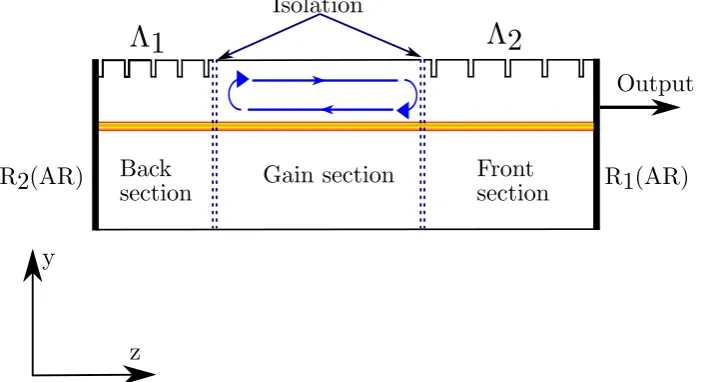
3.2 Slotted single mode laser with two electrically isolated sections. . . 32
3.3 y,z plane of the cavity structure, illustrating the various slot parameters. 33 3.4 Simulated TE field profile. . . 34
3.5 Contour plot of simulated amplitude reflection versus slot period order and slot width order for 20 slots, etched to 1.35 µm. . . 34
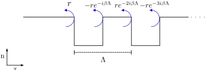
3.6 Schematic of a multiple period grating: in this case a three period grating. Individual colours correspond to the distinct grating periods. . 35
3.7 Reflectivity spectrum of a 1 and 3 period slotted grating. FSR reflection peaks are significantly reduces in amplitude in the 3 period grating. . . 36
3.8 Measured lasing spectrum of a laser with a one period grating (top) compared with a three period grating laser (bottom). The competing mode resulting from the FSR reflection peak is significantly suppressed in the three period grating laser. . . 36
3.9 Slotted vernier laser schematic. . . 37
3.10 Overview of the slotted laser diode fabrication process. The absence of any re-growth reduces the complexity and number of steps required. . . 39
3.11 SEM image of a slotted grating (bottom) and a single slot (top). . . 39
4.1 Experimental set up. . . 45
4.2 400 µm device performance. . . 46
4.3 SMSR of a 400 µm cavity length array of 12 lasers temperature-tuned over the C-band. SMSR is maintained close to or above 50 dB over the tuning range. . . 46
4.4 Wavelength tuning maps of differing cavity lengths. . . 48
4.5 SMSR map for a laser with 400 µm cavity length. . . 49
4.6 Wavelength tuning of a 1000 µm cavity length device. . . 50
4.7 Output power of a 1000 µm device. . . 51
xvii
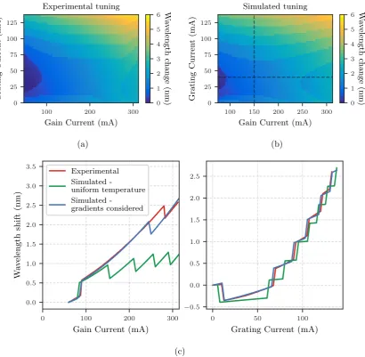
4.9 Experimental tuning map for a 1000 µm long laser cavity at 20◦C,
where black and red lines represent discontinuous and continuous
cur-rent paths, respectively. The red square corresponds to an ambient
temperature of 20◦C during athermal operation. . . 53
4.10 Wavelength tuning performance for continuous tuning scheme showing
wavelength stability (top), applied currents (middle), SMSR (bottom). 54
4.11 Wavelength tuning performance for the discontinuous tuning schemes
showing wavelength stability (top), applied currents (middle) and SMSR
(bottom) . . . 55
4.12 Output power (top), wall-plug efficiency (bottom) for (a) the
continu-ous tuning scheme with the output power stabilised using the SOA and
(b) the discontinuous tuning scheme. . . 56
4.13 Wavelength tuning performance for three lasers (numbers 1, 6 and 12)
in a 12-laser array at a heat sink temperature of 20◦C. For comparison, shaded regions represent the maximum spectral excursion of±12.5 GHz
allowed for a 50 GHz channel spacing next-generation passive optical
network 2 (NG-PON2) transmitter [47]. . . 57
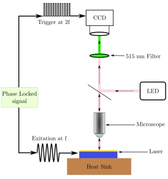
4.14 CCD-TR set up. . . 59
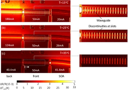
4.15 CCD-TR images: temperature profile of three section laser
operat-ing athermally at ambient temperatures of (a) 15◦C, (b) 25◦C and (c)
35◦C. Inset are the currents to each section to maintain athermal
per-formance. ∆R/R is the relative change in reflectivity and ∆T is the amplitude of the temperature increase from the ambient temperature
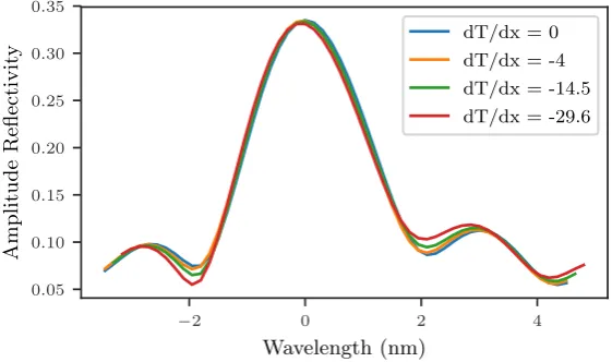
in each case. Magnified views of the grating sections are also provided. 60 4.16 Simulated grating reflectivity for experimentally measured thermal
gra-dients (mK µm−1), thermal gradients induced by the athermal tuning
have a negligible effect on the grating reflection spectrum. . . 61
4.17 Analytical simulation of laser behaviour: (a) experimental tuning map
for a 1000 µm long laser cavity at 20◦C, where black and red lines
represent discontinuous and continuous current paths, respectively, (b)
corresponding simulated map, (c) Wavelength shift across the paths
highlighted on (b), with and without temperature gradients. . . 65
4.18 Discontinuous tuning schemes, showing applied currents and SMSR found by (a) experiment and (b) simulation. . . 66
4.19 Wavelength tuning maps with a varying cleave error corresponding to
a phase change from 0π to 2π. Grey dashed line represents uniform
5.1 Basic principle of the time domain transfer matrix method. . . 70
5.2 Homogeneous segment. . . 71
5.3 Reflective interface, in our case this interface is a slot etched into the
waveguide ridge. . . 72
5.4 Comparison of 2D-SMM against 1D-TMM simulated spectrum.
Am-plitude reflection in the 1D case matches the 2D results well (Top).
Transmission of the 2D case only matches the one 1D case close to the
Bragg peak (Bottom). . . 73
5.5 Frequency response of the gain filter vs. experimental data. . . 76
5.6 TD-TMM algorithm. . . 79
5.7 Output spectrum of a 400 µm Fabry Pérot laser: simulated (top)
com-pared with experimental (bottom). . . 81
5.8 Simulated output spectrum of an array of 12, 700 µm cavity length lasers. 82
5.9 Simulated carrier and photon density profiles for lasers with cavity
lengths of 400 µm, 700 µm and 1000 µm, biased at 100 mA each. Solid
and dashed lines represent the gain and grating sections respectively. . 83
5.10 Simulated linewidth of a 400 µm slotted laser at 100 mA bias
cur-rent. Simulated linewidth of the laser is fitted to a Lorentzian with
FWHM = 3.74 MHz. Experimental data is fitted with a Voigt profile
with the Lorentzian component FWHM = 4.04 MHz . . . 84
5.11 Simulated linewidth of a 700 µm slotted laser at 100 mA bias
cur-rent. Simulated linewidth of the laser is fitted to a Lorentzian with
FWHM = 1.19 MHz. Experimental data is fitted with a Voigt profile
with an extracted Lorentzian component of FWHM = 1.29 MHz . . . . 85 5.12 Simulated (modified Schawlow-Townes equation) and experimental linewidth
of a 700 µm slotted laser. . . 86
5.13 Simulated (modified Schawlow-Townes equation) and experimental linewidth
of a 1000 µm slotted laser. . . 87
5.14 Simulated transient response of cavity lengths (a) 400 µm, (b) 700 µm,
(c) 1000 µm; each at 100 mA bias current. . . 90
5.15 Simulated radio frequency spectra. . . 91
5.16 Simulated modulation response for three differing laser cavity lengths. . 92
5.17 Simulated 3 dB bandwidth with varying cavity length. . . 93 5.18 Simulated eye diagrams for cavity lengths: (a) 400 µm, (b) 700 µm, (c)
1000 µm. . . 94
xix
5.20 Scanning electron microscope (SEM) image of a laser face on. Height of
different epitaxial layers can be seen, where the solder layer in particular
varies along the width of the chip. . . 99
5.21 Simulated and measured L-I curves of a 400 µm Fabry Pérot laser. . . . 100
5.22 Simulated (top) and experimental (bottom) L-I curves of a 700 µm length laser with increasing temperature. . . 101
5.23 Simulated and measured wavelength shift of a 400 µm cavity length laser.102
5.24 Simulated temperature of a 400 µm slotted laser compared to CCD-TR
measurements. . . 102
5.25 CCD-TR map of a 400 µm laser at 100 mA corrisponding to the
mea-surement in Figure 5.24. . . 103
5.26 Simulated and experimental lasing wavelength of 400 µm length single
mode lasers with one, two and three period gratings over a range of heat
sink temperatures. The temperature at which the lasing wavelength jumps increases with the number of periods used in the grating as a
result of increasing FSR peak suppression. . . 103
5.27 Wavelength map of a 400 µm length laser: simulation (top),
experimen-tal measurement (bottom). . . 105
5.28 Wavelength map of a 700 µm length laser: simulation (top),
experimen-tal measurement (bottom). . . 106
5.29 Wavelength map of a 1000 µm length laser: simulation (top),
experi-mental measurement (bottom). Star markers correspond to the
cur-rents simulated in Figure 5.30. . . 107
5.30 Carrier and photon density profiles within the grating section under varying gain section currents. Injecting the gain section is seen to
decrease the grating section’s carrier density. . . 108
5.31 Simulated power reflectivity, transmission and loss for a 9 slot grating
of period 80 µm. . . 109
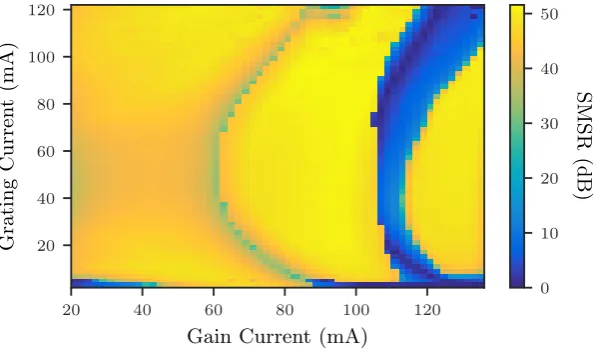
5.32 Experimental tuning map of wavelength (top) and SMSR (bottom). . . 110
5.33 Simulated tuning map of wavelength (top) and SMSR (bottom). . . 111
5.34 Simulated temperature distributions for the three supermodes labelled
in Figure 5.35. . . 112
5.35 Simulated profiles in the laser cavity for the three supermodes labelled in Figure 5.35, (top) temperature, (middle) photon density, (bottom)
carrier density. The Front/Back section currents for I, II and III are
265/180, 220/230 and 150/264 mA respectively with a constant gain
5.36 Individual contribution of physical effects to the overall tuning. . . 115
5.37 Simulated lasing spectrum for the three supermodes labelled in
Fig-ure 5.35. . . 115
5.38 Simulated tuning map of wavelength (top) and SMSR (bottom) for a
vernier laser biased uniformly at 300 mA with varying Front and Back section micro-heater power. . . 117
5.39 Simulated tuning map of wavelength (top) and SMSR (bottom) for a
vernier laser biased uniformly at 300 mA with varying Front and Back
section average temperatures. . . 118
5.40 Simulated SMSR map of micro-heater tuning (top) and direct current
injection (bottom) over an equivalent tuning range. Shaded regions are
below 40 dB. . . 119
5.41 Experimental tuning map of wavelength (top) and SMSR (bottom). . . 120
5.42 Simulated tuning map of wavelength (top) and SMSR (bottom) . . . . 121 5.43 Simulated lasing spectrum of a vernier laser tuned to two different
channels. . . 122
5.44 Experimental and simulated linewidth of a vernier laser with front and
back currents of 75 mA each; gain section current of 120 mA. . . 123
5.45 Experimental and simulated linewidth of a vernier laser with front and
back currents of 110 mA and 240 mA respectively; gain section current
of 120 mA. . . 124
6.1 Mirror loss, net gain and longitudinal mode positions with variables
relating to Equation 6.1. . . 130
6.2 Simulated SMSR versus wavelength detuning over one modespacing.
Red shading corresponds to SMSR below a defined minimum, and green
is above. . . 131
6.3 Simulated yield versus injection current for previously designed single
mode 700 µm cavity length laser. . . 131
6.4 SMM simulation of grating reflection (top) and transmission (bottom).
Slot width is constant at ∼ 1.1 µm (slot order of 4.5). . . 133
6.5 Flowchart illustrating the genetic algorithm. . . 136
6.6 Illustration of optimization process. Markers on each line represent spe-cific performance requirements. Figure (a) represents an unoptimized
case and figure (b) represents the optimized case where the various
requirements have been balanced against one another. . . 137
xxi
6.8 Convergence of population FOM (top) and the best solution within the
population (bottom). . . 143
6.9 Convergence of parameters represented by 2D histograms. The
popu-lation at generation 0 has a uniform distribution for each of the
param-eters — as the population evolves each parameter converges around a favourable value. . . 144
6.10 Simulated performance of the optimized and previous laser arrays:
slope efficiency (top), output power at respective operating current
(middle), operating current (bottom). . . 148
6.11 Operating current as a function of cavity length. . . 149
6.12 Simulated performance of the previous 700 µm cavity length array
de-sign and the optimized dede-sign: single mode yield (top) and maximum
operating temperature (bottom). . . 150
6.13 Experimental measurement of a 700 µm length laser designed for room temperature operation at 1536.36 nm (top), simulated spectra of a
700 µm length laser designed for room temperature operation at 1530 nm
and 1536.36 nm (bottom). . . 151
6.14 Simulated lasing spectra of the optimized lasers. . . 152
6.15 Fractional increase in operating current versus etch depth error. . . 153
6.16 Experimental measurement of a 1000 µm cavity length laser designed
for∼ 1533 nm lasing wavelength. The laser is biased at 100 mA with a
heatsink temperature of 25◦C. . . 154
6.17 Simulated performance of the previous 1000 µm cavity length array
design and the optimized design: slope efficiency (top), output power at respective operating current (middle), operating current (bottom). . 155
6.18 Simulated performance of the previous 1000 µm cavity length array
design and the optimized design: single mode yield (top) and maximum
operating temperature (bottom). . . 156
6.19 Simulated lasing spectra: previous 1000 µm cavity length design (top),
optimized laser design (bottom). . . 157
6.20 SMM simulated grating reflection and transmission spectra: previous
design (top), optimized laser design (bottom). . . 158
6.21 Distribution of parameters during optimization of a low linewidth laser. Red line represents parameters of the best individual in a given
6.22 Simulated linewidth of the optimized design. A waveguide loss of
28 cm−1used in the optimization corresponds to the most recent
waveg-uide loss measurement, wavegwaveg-uide loss of 18 cm−1 corresponds to the
lowest waveguide loss which has been measured for our devices. . . 160
6.23 Simulated lasing spectrum, biased at 265 mA. . . 161 6.24 Distribution of parameters during optimization of a directly modulated
laser. Red line represents parameters of the best individual for a given
generation. . . 163
6.25 Simulated modulation response of the optimized DML. . . 164
6.26 Simulated eye diagrams of the optimized DML at 28 GBd symbol rate
at a constant active region temperature of 25◦C under varying bias
currents. . . 165
6.27 Simulated eye diagrams of an optimized DM laser modulated at 28
GBd symbol rate for a range of active region temperatures. . . 166
7.1 Potential athermal grating design. . . 171
7.2 Simulated linewidth of a Vernier laser with a gain section length of
1000 µm. . . 173
B.1 Stabilization algorithm. . . 178
B.2 Result of applying the stabilization algorithm. Artefacts near edge
xxiii
List of Tables
3.1 Specifications for the IQE wafer. . . 40
4.1 Mean temperatures across the gain and SOA section, along with the
resultant temperature gradient across the grating section. . . 59
4.2 Analytical model parameters . . . 62
5.1 TD-TMM model parameters . . . 77 5.2 Physical parameters for each layer. . . 98
6.1 Genetic algorithm parameters. Ng is the number of free varying genes. 139
6.2 Example of a multiple period grating composition. . . 139
6.3 Initial population specifications. . . 140
6.4 Optimization result for a single laser at 1550 nm. . . 141
6.5 Optimization results for varying linewidth requirements. . . 143
6.6 Optimization results for varying output power requirements. . . 145
6.7 Linewidth requirements for a range of modulation formats [77]. . . 159
C.1 Optimization 1. . . 182 C.2 Optimization 2. . . 183
C.3 Optimization 3 — Lower single mode yield. . . 184
C.4 Optimization results, 0.5 MHz. . . 185
C.5 Optimization results for low linewidth laser. . . 186
xxv
List of Abbreviations
AR / HR Anti-Reflective / High-Reflective
CCD Charge-Coupled Device
CCD-TR CCD Thermo-Reflectance
CW Continuous Wave
DBR Distributed Bragg Reflector
DCN Data Centre Network
DFB Distributed Feedback
DWDM Dense Wavelength Division Multiplexing
EA Electro Absorption
EDFA Erbium Doped Fibre Amplifier
FEM Finite Element Method
FOSS Free and Open Source Software
FSR Free Spectral Range
FWHM Full Width at Half Max
ICP Inductively Coupled Plasma
IIR Infinite Impulse Response
ITU-T International Telecommunication Union-Telecommunication
Laser Light Amplification by Stimulated Emission of Radiation
LED Light Emitting Diode
LIV Light Current Voltage
MQW Multiple Quantum Well
ONU Optical Network Unit
OOK On-Off Keying
OSA Optical Spectrum Analyser
PKS Phase-shift Key Modulation
PIC Photonic Integrated Circuit
PON Passive Optical Network
QAM Quadrature Amplitude Modulation
QCSE Quantum Confined Stark Effect
QW Quantum Well
SCH Separate Confinement Heterostructure
SEM Scanning Electron Microscope
SG-DBR Sample Grating Distributed Bragg Reflector
SMSR Side Mode Supression Ratio
SMM Scattering Matrix Method
SOA Semiconductor Optical Amplifier
TEC Thermo-Electric Peltier Cooler
TMM Transfer Matrix Method
xxvii
Physical Constants
Speed of Light c0 = 2.997 924 58×108m s−1
Elementary charge q= 1.602 176 620 8×10⁻¹⁹C
1
Chapter 1
Introduction
1.1 History of Optical Communications
The 1960s saw the emergence of two key advances that would make high speed optical
communications feasible. The first of these was the development of the semiconductor
laser diode by Hall et al. [1] in 1962 . These early homojunction laser diodes only
functioned at ∼ 80 K and as a result were not suitable for any practical uses. With
the development of liquid phase epitaxy (LPE), the first heterojunction lasers were fabricated, bringing semiconductor lasers closer to room temperature operation. It
was not until the development of double heterostructure lasers that room
tempera-ture operation was realized in 1970 [2]. Double heterostructempera-ture lasers were rapidly
commercialized for a variety of uses including optical communications. The second
ad-vancement which allowed for long distance communication based on optical signals was
the development of a suitable material to transport light signals. This breakthrough
was achieved in 1966 with the proposal of a method to improve fibre performance by
removing impurities in glass which otherwise led to high attenuation in the order of
1000 dB km−1 [3]. By 1970, optical fibers with attenuation of ∼ 20 dB km−1 — low enough for communication purposes — were successfully developed by Corning Glass
Works Inc.
These advancements heralded the deployment of the first fibre-optic networks —
implemented over a range of wavelengths. In 1978, the firstfibre-to-the-home solution using multi-mode fibers at 850 nm, as part of Japan’s Hi OVIS project, was deployed.
Soon thereafter, 1300 nm systems using single-mode fibres were implemented in 1981.
By 1984 the first submarine fibres had been deployed by British Telecommunications
PLC. Due to fibre attenuation, many of these early fibre networks relied on optical
repeats for signal regeneration, making network deployment and upkeep costly [4].
systems are based. The optical gain exhibited by EDFAs in the 1550 nm region saw
the implementation of optical communication predominantly in the c-band (1530 to
1565 nm). Crucially, EDFAs allowed for the transmission of long reach signals without
the need for signal regeneration, previously a barrier to widespread deployment.
Signal Direction
Laser array Multiplexing De-Multiplexing
Input Data Detection
Figure 1.1: Wavelength Division Multiplexing.
In conjunction with EDFAs, the development of non-zero dispersion shifted fibres
and dispersion management enabled a key technology of modern optical
communi-cation systems: wavelength division multiplexing (WDM). WDM transmits data in parallel by using several optical carriers each at a specific wavelength, as shown in
Fig-ure 1.1. The ability to send multiple signals over a single fibre has yielded dramatic
increases in data rates. Dense wavelength division multiplexing (DWDM), a form
of WDM with closely spaced carriers, is now commercially available achieving data
rates upward of 20 Tb/s, and forms the backbone of modern optical communication
networks [4, 5].
1.2 Challenges in modern optical networks
Despite the significant pace of progress, contemporary optical communication
net-works face a growing challenge in meeting the ever-increasing demand for data
band-width. Data intensive services such as video streaming, cloud and gaming are
cur-rently causing acapacity crunch, driving a need for increases in data rates. Numerous emerging technologies, such as the internet of things and self driving cars also have
the potential to dramatically increase network congestion often in unpredictable ways.
In general, modern optical networks can be categorised by their transmission distance
into short reach and long-haul networks each of which face unique challenges with
1.2. Challenges in modern optical networks 3
1.2.1 Short reach networks
Short reach networks generally have transmission distances on the order of tens of
kilometres. Short reach networks include access networks which connect end users to
the metro and core. Access networks have in recent years seen significant adoption
of optical networking in place of electrical, with a view to increasing capacity. In
order to support a larger number of end users, access networks have sought to employ
WDM passive optical networks (PON). WDM-PON, with channel spacing generally
≤ 100 GHz is seen as a key technology in expanding access capacity. By using a
larger number of tightly spaced optical carriers, a larger number of end users can
be supported at high data rates. However, with increasing spectral density the risk
of channel crosstalk increases and as a result, each optical transmitter needs to be carefully controlled such that each carrier is at the appropriate wavelength. In
partic-ular, the thermally induced wavelength shift associated with semiconductor lasers is a
challenge for DWDM systems. Given the large number of user optical network units
(ONUs) required for fibre to the home applications, inventory cost also becomes a key
factor. As such, balancing the performance and cost of optical components represents
a crucial factor in the adaptation of PON access networks.
Another short reach network, which has seen significant growth, is that of
inter-and intra-data centre networks (DCNs). In order to increase efficiency inter-and capacity
within data centres, electronic components will increasingly be replaced by optical solutions. Such architectures have been proposed with high energy efficiency, however,
the use of optical components generally increases deployment cost [6]. Additionally, as
data centres typically have size constraints, the spatial footprint of optical solutions
becomes critical. Form factors such as C form-factor pluggable (CFP), consisting
of several discrete optical components were rather large for DCN applications. In
recent years, CFP2 and CFP4 have leveraged improved optical integration to double
and quadruple port density over the original CFP [4]. In order to further reduce
spatial footprint and cost, research into monolithic photonic integrated circuits (PICs)
continues, seeking to integrate more optical components on a single chip. As photonic devices begin to be integrated at higher densities, thermal management again becomes
an important consideration. As a result, there is a need for a detailed understanding
of individual components’ thermal behaviour, as well as new thermal management
techniques. The viability of such PICs depends largely on the cost and reliability of
the individual components therein and thus considerable effort is being undertaken
1.2.2 Long-haul networks
Long-haul networks include metro and core, with transmission distances of hundreds
or thousands of kilometres. In such networks, cost and power consumption are less
critical than in short reach networks. Long-haul networks specifically face challenges
in maximizing spectral efficiency and transmission distance. New high cardinality
modulation formats in particular seek to improve spectral efficiency of long-haul
net-works. As core networks are already widely deployed, future advances in this context
will likely focus on utilizing existing infrastructure in more efficient ways. Further
ad-vancements may also include: the implementation of integrated arrays for modulation
and coherent reception, optical comb spectrum generation, and transponders capable
of flexible data rates, tuned to required distance are also likely to be implemented in the coming years [4].
1.2.3 Advanced modulation formats
In order to further increase data capacity of WDM systems, increases in spectral
efficiency are required in both short reach and long-haul networks. Limited by
con-ventional modulation such as on-off keying (OOK), recent development of advanced
modulation formats has yielded dramatic improvements in capacity. Such
modula-tion formats allow for the encoding of multiple bits of data during a given symbol for
a given wavelength channel, resulting in improved data rates per wavelength
chan-nel [4]. Phase-shift keying key modulation (PSK) is a widely implemented modulation
technique which uses coherent detection to encode data in amplitude and phase. Com-mercially available formats include binary PSK, quadrature PSK, and 16-quadrature
amplitude modulation (QAM) [4]. Figure 1.2 shows the main dimensions along which
such coherent communication can increase capacity. In order to reach higher order
constellation multiplicity, achieving low linewidth is a key goal for laser diodes.
Prior to more advanced coherent modulation, formats based on intensity
modula-tion and direct detecmodula-tion (IM-DD) were the status quo. The emergence of coherent
communication resulted in a shift of research focus away from IM-DD formats.
How-ever, the capacity crunch in short haul applications has seen a resurgence in research
into IM-DD formats. Such formats offer cheap and energy-efficient alternatives to co-herent detection, suitable for short reach networks. Advanced IM-DD formats include
multi-level schemes such as 4 level pulse amplitude modulation (4-PAM) which have
1.3. Tunable laser diodes 5
Figure 1.2: Dimensions along which capacity can be increased in co-herent communication (from Agrell et al. [4]).
In order to facilitate increased capacity there is a need for next generation PIC
components, in particular semiconductor laser diodes and EA modulators, to be com-patible with cutting edge and emerging modulation formats.
1.3 Tunable laser diodes
Semiconductor laser diodes represent an essential optical component within optical
networks, as they generate the optical carrier signal for the transmission of data. Given
the frequency grid spacing defined by the international telegraph union
telecommu-nication standardisation sector (ITU-T) of 12.5 GHz to 100 GHz and wider, DWDM systems can exceed 80 individual wavelength channels [7]. Such a large number of
wavelength channels means that having an individual laser for each channel is not
economically feasible. Instead, lasers capable of tuning to several channels are used,
reducing the number of lasers required for a DWDM system. Several types of tunable
lasers are used in current networks. As single lasers generally have tuning ranges on
the order of nano meters, one approach is to combine several such lasers together with
their combined tuning range covering the desired wavelength channels. Such early
tunable laser arrays were demonstrated by Kudo et al. [8] in the 1990s, achieving
15.3 nm tuning range. More recent tunable arrays are now capable of fully covering the C-band [9]. Higher tuning ranges can be achieved by individual lasers, albeit
with more complicated designs. Sample grating DBR (SG-DBR) lasers use several
interrupted grating sections to generate super-modes, thereby extending the tuning
[10], achieving 57 nm tuning with more than 30 dB SMSR. SG-DBR lasers are also
capable of integration with other photonic components. Mason et al. [11] integrated
SG-DBR lasers with SOAs to achieve output powers > 8 Bm and Akulova et al. [12] integrated EA modulators allowing for error-free transmission at 2.5 Gb/s for 350 km.
Such SG-DBR lasers are now widely deployed in optical networks as a flexible wave-length source. Modulated grating Y-branch (MG-Y) lasers also tune via the vernier
effect in order to obtain an extended tuning range. These lasers differ from SG-DBRs
by having both gratings located on the same side of the gain section, thus avoiding
the output light passing through the front reflector and being attenuated. Such lasers
have been developed, attaining SMSR ≥ 40 dB, high output power ≥ 13 Bm and a
low power variation < 1.5 dB [13]. A detailed review of the aforementioned tunable lasers can be found in Coldren et al. [14].
For the next generation of long haul communications new lasers designs capable
of full band tunability, such as the digital supermode (DS)-DBR laser, have been investigated to replace fixed channel DFBs, achieving similar performance in terms of
power and SMSR [15].
Although existing tunable laser solutions have achieved wide use in optical
com-munications they generally involve complex and expensive fabrication. In long-haul
systems where the price point of optical components do not have as large of a
foot-print, such complex lasers — fabricated through epitaxial re-growth, embedded
grat-ing structures and high resolution epitaxy — are well deployed and have become the
de facto solution. However, as optical communication penetrates further into short
reach networks and the number of devices increases, inventory cost begins to play a
larger role and the mature laser designs suitable for established networks may not be ideal for emerging demands. There has been a concerted effort to reduce costs of these
components while also maintaining efficiency as well as integrating more components
on a single chip.
A key area of interest which has emerged is replacing embedded gratings with
surface etched gratings. This removes the need for the aforementioned re-growth and
high resolution epitaxy with a view to driving down costs. Recently, Yang et al.
[16] demonstrated a monolithic PIC comprised of tunable single mode lasers, SOAs
and multi-mode interference (MMI) couplers, using a simple slotted grating design.
Cheap widely tunable lasers have also been demonstrated using a monolithic slotted
grating design, demonstrating linewidth ≤ 800 kHz and fast wavelength switching
between channels [17]. Surface grating laser designs have also been simulated for
potential direct modulation applications in the 1.3 µm window, achieving a predicted
1.4. Thesis scope and goals 7
implemented in silicon photonics with an InGaAsP-Si hybrid single-mode laser based
on slotted silicon waveguides achieving good performance with a threshold current of
21 mA, output power of 1.9 mW and side-mode suppression (SMSR)≥35 dB [19]. The
common themes of these recent efforts are low cost, simple fabrication, and monolithic
integration. All of these attributes are increasingly seen as important for laser diodes to enable the next generation of optical communication networks.
1.4 Thesis scope and goals
With the above context and challenges in mind, research into cheap, simply fabricated,
monolithic laser designs has been previously undertaken within the Trinity College
Dublin semiconductor photonics (TCDSP) group. Out of this research, a platform
for low cost laser diodes based on surface etched gratings has been developed. These
lasers are designed to reduced cost in a number of ways. The ability to integrate the lasers with a range of optical components helps increase the number of functions
per package thus reducing cost. In addition, the slotted grating simplifies
manufac-turing, potentially increasing yield and allowing for cheaper manufacturing methods.
(Detailed costing in relation to the high-order surface grating laser have not been
carried out by our group and for companies who sell lasers with similar structures,
this information is proprietary and confidential.)
Most recently, the TCDSP group has demonstrated tunable laser arrays based
on high order surface etched gratings, capable of covering the C-band and achieving
linewidths compatible with advanced coherent modulation formats: star 16QAM and 8PSK [20]. In addition, lasers with monolithically integrated components in the form
of SOAs and electro absorption modulators have been demonstrated using this
plat-form [21, 22]. Widely tunable lasers based on the vernier effect were also fabricated
achieving > 50 nm tuning range with SMSR ≥ 30 dB for the majority of this range [23].
From this preceding work, a number of issues were highlighted. Chief among these
was a need to understand in greater detail the physical behaviour observed in the
fabricated devices. Of particular interest is the wavelength tuning behaviour of said
lasers as well as the thermal dynamics underlying said tuning. In addition, areas where performance could be improved were identified and this thesis focuses on addressing
these with a view to designing new slotted lasers with improved performance. With
the above in mind, the overarching goals of this thesis are to:
• Develop a high fidelity numerical model capable of explaining and predicting laser tuning behaviour as well as overall device performance.
• Iterate upon previous designs to improve performance of laser diodes for the next fabrication run.
With regard to the final goal above, design procedures for surface grating based
lasers in the extant literature tend to rely on an ad hoc approach, simulating grating
properties such as reflectivity over a limited range of design variables and choosing
a suitable grating. A generalized approach to surface grating optimization is lacking
and to our knowledge an efficient method fully covering the various design variables for a slotted grating while also encompassing the complexities introduced by them
has not been demonstrated. As such, this thesis sets out to define an improved
method whereby slotted grating laser diodes can be rigorously optimized, taking all
degrees of freedom into account while being applicable for arbitrary laser performance
requirements.
Thus far, attention has been focused on lasers within the context of optical
com-munication networks. In addition to optical comcom-munications, semiconductor laser
diodes have a number of wide-ranging applications, such as gas detection,
measure-ment systems and atomic clocks. The slotted laser diodes presented herein also have potential application in these fields, though this research is primarily undertaken in
9
Chapter 2
Semiconductor Lasers
2.1 Introduction
Semiconductor laser diodes — as well as lasers in general — require a number of basic
elements in order to operate. These include a:
• Gain medium.
• Pump source.
• Feedback mechanism, i.e. a mirror.
• Wavelength / frequency filter (single mode case).
A gain medium is required for the amplification of light through stimulated
emis-sion. In order for the gain medium to support stimulated emission, a pump source
— generally optical or electrical — is needed to excite electrons to a higher energy
level. Once excited, electrons can decay to a lower energy via stimulated emission,
resulting in gain. In order for lasing to occur, the gain within a laser must be greater
than the losses. To this end, a feedback mechanism is required to overcome loss from
the gain medium. Typically, two mirrors fulfil this requirement, forming a cavity in which light is confined. Once an optical mode within a cavity has more gain than loss,
lasing will occur. Laser cavities generally support a multitude of longitudinal modes
at a number of wavelengths. In order to select a single cavity mode, a mechanism for
filtering out competing modes is needed, normally in the form of a grating. These
concepts will be introduced in this chapter, as well as common semiconductor laser
diode structures and important properties thereof.
2.1.1 Energy bands in solids
the progression of energy levels with an increasing number of atoms N. At low densities, as found in gases, energy levels of the electrons are discrete and are in effect
the same as a single isolated atom. Moving away from this isolated atom case, as
the number of atoms increases, the energy levels of the electrons of each atom are
perturbed resulting in energy splitting. This splitting repeats itself as the number of atoms increases and in the case of a large number of atoms, as in solids, the
discrete energy levels effectively becomes a continuous energy band. The splitting
of the highest occupied atomic energy level forms the valence band with the next
higher atomic level splitting to form the conduction band. Between the valence and conduction band there exists a band gap, which no electron can occupy.
N atoms
Energy
E1
E2
Valence band Conduction
band
Band gap
Figure 2.1: Change of energy levels from the single atom case to the band structures of crystals.
Plotting the valence and conduction band energy levels against their respective
wave-vectors results in the band structure of semiconductors as shown in Figure 2.2.
An important result of the E versus k diagram in Figure 2.2, is that not all energy levels can transition between one another, with energy transitions largely limited to vertical transitions only involving energy transfer. This is due to the fact that any
other transition will involve a change in momentum k, and as the momentum of
photons involved in these transitions is small compared with the momentum available
to electrons and holes in bands, such transitions have a low probability. As a result,
materials with direct band gaps, where Ec and Ev coincide at the same wavevector k, are required in order for optical transitions to occur efficiently between the bands. The region where light is generated through stimulated emission in a laser, known as
the active region, is thus predominantly engineered with direct band gap materials.
2.1. Introduction 11
k
E
Ev
Ec
Figure 2.2: Electron energy vs. wave vector magnitude in a direct band gap material.
2.1.2 Heterostructures
In order to enable the operation of semiconductor lasers, the previously described
band structures of solids can be engineered in numerous ways. Modern semiconductor
lasers are based on the principle of a double heterostructure. In this scheme an active region is sandwiched between two layers of higher band gap energy. Figure 2.3 shows
a simplified band structure of a double heterostructure in forward bias. Due to the
high band gap confinement layers either side of the active region, electrons cannot
escape into the p-type confinement layer and the holes cannot escape into the n-type
layer. As such, they are forced to recombine in the active region.
E
FvE
FcE
cE
Vp-type
confinement
n-type
con
fi
nement
hv
Figure 2.3: Double heterostructure band structure.
Decreasing the width of the active region close to or smaller than the de Broglie
This quantization has the effect of increasing the effective band gap energy as well
as modifying the density of states as shown in Figure 2.4. The step-like behaviour
increases the differential gain as the injected carriers have a narrower energy range.
The gain can further be increased by introducing strain in the active region. This has
the effect of reducing the density of states at the top of the valence band, allowing for population inversion to be obtained at a lower carrier density [24].
Although the carrier confinement is high in quantum wells, their narrow width
means that optical confinement is relatively poor. To improve the optical
confine-ment, separate confinement heterostructure quantum well (SCH-QW) structures are
used. Such SCH-QWs have an additional waveguide around the quantum well,
improv-ing optical confinement. Finally, utilisimprov-ing multiple quantum wells (MQW), whereby
several QWs are grown in series, further increases the optical gain. A strained
SCH-MQW structure composed of five QWs forms the active region for all the proceeding
results shown in this thesis (see Table 3.1, chapter 3 for details).
Density of states,ρ
Energy
,
E
Bulk
Quantum well
2.1. Introduction 13
2.1.3 Recombination and rate equations
Recombinationhv
R
sphv hv
R
stim Ez
R
nr = Electron= Hole
Figure 2.5: Primary paths of electron-hole recombination: spontaneous emission (Rsp), stimulated emission (Rstim) and non-radiative
recom-bination (Rnr).
The two main light generating processes in laser diodes are spontaneous and
stim-ulated emission. With the previously quantum well band structure in mind, these
processes can be understood as shown in Figure 2.5. A detailed description of these processes is available in Coldren, Corzine, and Mashanovitch [25], from which the
definitions in the following three paragraphs are sourced.
In the case of spontaneous emission (Rsp), an electron in the conduction band
spontaneously decays to the valence band. The process of spontaneous emission is
random by nature with random direction and phase, resulting in incoherent emission.
This is the primary source of light in light emitting diodes (LEDs). The probability
of a spontaneous recombination event occurring is proportional to the number of
electrons (N) times number of holes (P), N ×P. As the total charge in undoped
active regions remains constant, the spontaneous recombination rate is proportional to N2.
The process of stimulated emission (Rstim) is also shown in Figure 2.5. An incident
photon of energyhvperturbs the system, stimulating the recombination of an electron and hole with the generation of a new photon. Importantly, both photons have the
same amplitude and phase. As this process cascades throughout the laser cavity,
coherent light is created with high intensity.
In addition to radiative recombination, non-radiative recombination (Rnr) provides
an alternate path through which conduction band electrons may decay. There are
surfaces, and interfaces. This category of non-radiative decay is proportional to the
number of carriers N. On the other hand, Auger recombination involves an excited
conduction band electron decaying to fill a valence band hole. This differs from
spontaneous emission because the energy is transferred as kinetic energy to another
conduction band electron. In this case the process requires two electrons and a hole, and as a result is proportional to N3.
Rate equations
In order for lasing to occur in a diode, there needs to be a population inversion, i.e.
the number of electrons in the conduction band needs to be greater than the number
in the valence band. This can be achieved by electrically pumping electrons from the
valence band into the conduction band. Once this occurs, spontaneous emission will increase and seed the stimulated emission needed for lasing. In semiconductor lasers,
electrically pumping the active region leads to an increase in carrier density given by
Ggen= Iηi
V q, (2.1)
where I is the injection current, ηi represents the injection efficiency, q is elementary
charge andV is the active region volume. Combining the rate of carrier injection with the previously described possible paths of decay gives the rate equation
dN dt =
Iηi
qV −(AN +BN
2+CN3+Rstim), (2.2)
where A, B, C are the coefficients of non-radiative, bimolecular (spontaneous) and Auger recombination respectively [25]. The rate equation determines many of the
dynamics of laser behaviour, both static and transient.
2.2 Fabry Pérot laser
The final requirement for a laser is longitudinal light confinement in the form of
a cavity. The simplest case of this is a Fabry Pérot laser which is illustrated in
Figure 2.6. In this device, light is confined to the gain medium by two reflecting surfaces. r1 and r2 are the amplitude reflectivity of the two cleaved facet mirrors, P1
2.2. Fabry Pérot laser 15
r1 r2
Gain Medium P2
P1
U(x,y)
y z
Figure 2.6: Fabry Pérot laser schematic.
in the cavity can be described by the propagation constant β:
β =κ0n0ef f +jgnet
2 (2.3a)
gnet =gΓ−αi, (2.3b)
whereαi is the waveguide loss, Γ is the confinement factor,gnet is the net modal gain
and κ0 is the free space propagation constant (κ0 = 2λπ) [25]. To achieve lasing, the net gain over a single round trip must equal the net loss, which includes the loss at the reflective boundaries r1 and r2. This will occur when
r1r2e−2iβL = 1, (2.4)
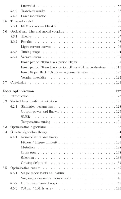
where L is the length of the Fabry Pérot cavity. Once this condition is met the laser is considered to be above threshold. Figure 2.7 shows the main changes when moving
from a below threshold regime to an above threshold regime. Below threshold, carrier density in the active region increases with injection current. The carrier density will
continue to increase until the gain is large enough to satisfy Equation 2.4. Once this
occurs, the output power abruptly increases and the carrier density clamps at the value
at threshold, as any additional carriers injected immediately decay via the stimulated
emission which now dominates the light creation process within the QWs. The current
at which this occurs is known as the threshold current (Ith) with a corresponding
threshold carrier density of (Nth) as shown in Figure 2.7. Once above threshold, the
output power increases approximately linearly. From Figure 2.7 the slope efficiency
can be defined as the differential change in output power for a change in input power,
ηse = ∆P
measured in units of mW mA−1 [25]. It should be noted that the carrier density along
the cavity is non-uniform and Figure 2.7 represents the approximate carrier density
behaviour averaged over the length of the cavity.
Figure 2.7: Typical threshold behaviour of a laser diode.
The lasing spectrum from a Fabry Pérot laser is largely determined by the
cav-ity length. Wavelengths which have a constant phase after one round trip will add
constructively and lase. The wavelengths which satisfy this condition are given by
λm = 2· n 0
ef fL
m , (2.6)
where m∈Z.
Figure 2.8 shows this condition where the vertical lines represent solutions to
Equation 2.6 for an arbitrary cavity length. The wavelength of the longitudinal
modes relative to the modal gain curve (green) will determine the power of each
lasing mode. The gain curve plotted in Figure 2.8 was calculated using the parabolic
approximation given in Westbrook [26]. An experimentally measured spectrum of a
400 µm long Fabry Pérot cavity is also shown in Figure 2.8 (bottom). The spectrum
is strongly multi-mode, which is generally not suitable for optical communications.
To obtain a single lasing wavelength, a method whereby competing modes are
fil-tered out is required. This can be achieved by incorporating grating structures, which
[image:46.595.178.395.170.300.2]2.3. Single mode lasers 17
−200 −100 0 100 200 300 400
Mo
dal
Gain
(cm
−
1)
Longitudinal Modeλ Modal Gain
1520 1530 1540 1550 1560 1570 1580
Wavelength (nm) −60
−50 −40 −30 −20 −10
Output
P
ow
er
(dBm)
Figure 2.8: Fabry Pérot cavity’s possible longitudinal modes and gain curve (top). Measured 400 µm Fabry Pérot lasing spectrum at 60 mA
(bottom).
2.3 Single mode lasers
The multi-mode spectrum produced by Fabry Pérot lasers has a number of negative
properties which make it ill-suited for fibre-optic communications. Considering a
wavelength multiplexing system in which a number of independent signals need to be carried on their own unique wavelength, it is clear multi-mode spectra are not
suitable. In addition, the dispersion which light experiences in optical fibres limits
the use of Fabry Pérot lasers. In order to overcome dispersion it is necessary to
produce a spectrally pure source with a narrow linewidth via single mode lasers.
Grating structures play a pivotal role in enabling such single mode lasers.
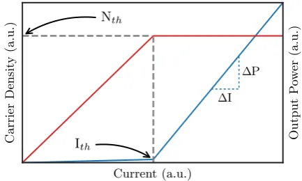
2.3.1 Gratings
A grating consists of a periodic structure from which reflections add up constructively
at a particular wavelength known as the Bragg wavelength. In laser diodes, these
gratings take the form of structural variations which cause variations in the effective
n z
Figure 2.9: Typical grating structure, where changes in refractive index profile results in reflection.
of n1 to one ofn2 can be approximated by the Fresnel equation as
r12 ≈ n1−n2
n1+n2. (2.7)
The periodicity of these reflections determines which wavelengths will be in phase upon
reflection and add constructively, and which will be out of phase and add destructively.
This is known as the Bragg condition and is described by the equation
λBragg= 2nef fΛ, (2.8)
whereλBraggis the Bragg wavelength, Λ is the grating period andnef f is the effective
index of the fundamental mode [25]. Such a grating structure matching the Bragg
condition is illustrated in Figure 2.9. The reflectivity peak of a grating can be tuned
to a desired wavelength via the equation
Λ = λ
2nef f
·m, (2.9)
wherem∈Z. The integer m will be referred to as theorder of the grating henceforth. The result of these constructively interfering reflections is a Bragg peak as shown in
Figure 2.10. Generally, the bandwidth of such a Bragg peak is engineered to be
narrower than the spacing of the longitudinal modes, ensuring that only one mode is supported by the cavity.
Semiconductor laser designs are generally categorized by the type of grating
struc-ture which they utilize. Two examples of single mode lasers which use different
grat-ing structures are distributed feedback lasers (DFBs) and distributed Bragg reflector
lasers (DBRs) as shown in Figure 2.11a and 2.11b. In the case of the DBR laser, a
[image:48.595.113.456.102.217.2]2.3. Single mode lasers 19
1540.0 1542.5 1545.0 1547.5 1550.0 1552.5 1555.0 1557.5 1560.0
Wavelength (nm)
0.0 0.2 0.4 0.6 0.8 1.0
Amplitude
Reflection Transmission
Figure 2.10: Bragg peak resulting from a periodic change in refractive index.
r1
Grating
Active region
r2
(a)
r1 rg(λ)
Grating Gain section
λBragg
Phase section (b)
Figure 2.11: Longitudinal cavity cross sections of (a) DFB and (b) DBR lasers.
laser. The reflection peak of this grating will have