SYS68K/ DRAM-E3Ml
HARDWARE USER'S MANUAL
32 BIT DYNAMIC MEMORY BOARD
WITH FME INTERFACE
2nd Edmon
September 1985
PART NO. 800043
FORC~ COMPUTERS Inc./GmbH All Rights Reserved
This document shall not be duplicated. nor lis contents used for any purpose, unless express permission has been gran1ed.
NOT E
The information in this document has been carefully checked and
is believed to be entirely reliable. FORCE COMPUTERS makes no
warranty of any kind with regard to the material in this
document, and assumes no responsibility for any errors that may
appear in this document. FORCE COMPUTERS reserves the right to
make changes without notice to this, or any of its products, to
improve reliability, performance or design.
FORCE COMPUTERS assumes no responsibility for the use of any
circuitry other than circuitry which is part of a product of
FORCE COMPUTERS GmbH/Inc.
FORCE COMPUTERS does not convey to the purchaser of the product
described herein any license under the patent rights of FORCE
COMPUTERS GmbH/Inc. nor the rights of others.
FORCE COMPUTERS Inc. 727 University Avenue Los Gatos, CA 95030 U.S.A.
Phone Telex FAX
: (408) 354 34 10 172465
(408) 395 77 18
FORCE COMPUTERS GmbH Daimlerstrasse 9
D-80l2 Ottobrunn/Munich West Germany
Phone Telex FAX
(089) 6 09 20 33 : 5 24 190 forc-d
(0 89)6 09 77 93
FORCE COMPUTERS FRANCE SarI 11, rue Casteja
92100 Boulogne France
Phone Telex Fax
(1) 620 37 37 206 304 forc-f : (1) 621 35 19
Table of Contents
1.0 General Information ••
2.0 General Operation . . . .
Hardware Description •••••••••••
Supported Transfer Types •••••••
. .
. .
.
..
Access to the DRAM-E3Ml Board.. • ••••
3.0 3.1 3.2 3.2.1 3.2.2 3.3 3.4 3.5 3.6 3.7 3.8
The Access Address Selection of the DRAM-E3Ml Board ••• Modification of the Access Address of the DRAM-E3Ml ••• The Address Modifier Decoding •••
The Parity Check ••
The Access Times •••••••••••• The Refresh ••••••••••••••••• The Battery Back-up Option ••• The Front Panel •••••••••••••••
4.0 4.1
The FMEbus Interface ••••••••••••••••••••••••••••• Access Address Selection using FME Slave Boards ••
5.0 5.1
Preparation for Use ••
Power On •.••••••••••.
APPENDIX A
·
.
. . .
SpecificationAPPENDIX B
· . . .
. .
.
.
.
.
Component PartAPPENDIX C
·
.
.
.
. .
.
.
. .
Description ofSYS68K/DRAM-E3Ml
List DRAM-E3Ml
the Jumperfields
APPENDIX D
· . . .
.
.
.
.
Circuit SchematicsAPPENDIX E
· . . .
.
. .
.
Connector PIN AssignmentsAPPENDIX F
· . . .
Product Error ReportList of Figures
Page
Figure 1 Photo of the SYS68K/DRAM-E3Ml... 8
Figure 2 Block Diagram SYS68K/DRAM-E3Ml . . . 10
Figure 3 The Decoding Logic Block Diagram . . . 15
Figure 4 Location Diagram of the Access Address Selection Jurnperfields. . . . . 16
Figure 5 The AM-Code Jumperfields . . . 25
Figure 6 Parity Check Jumperfield Locations . . . 37
Figure 7 Location Diagram of the Battery Backup Jumperfields. . . . . 41
Figure 8 The Front Panel of the SYS68K/DRAM-E3Ml . . . 43
Figure 9 The FME C o n c e p t . . . 45
List of Tables
Page
Table 1 Supported Data Transfer Types •••••••••••••••••••• 12
Table 2 Jumperfield Assignment to Access Address
Selection. . . . . 17
Table 3 Default Access Address Selection ••••••••••••••••• 18
Table 4 Access Address Selection Example 1 ••••••••••••••• 2121
Table 5 Access Address Selection Example 2 ••••••••••••••• 21
Table 6 Access Address Selection Example 3 ••••••••••••••• 22
Table 7 Access Address Selection ••••••••••••••••••••••••• 23
Table 8 The Address Modifier Codes ••••••••••••••••••••••• 26
Table 9 The AM Code S e l e c t i o n . . . 28
Table 1121 Default AM Code Selection •••••••••••••••••••••••• 3121
Table 11 AM Code Selection Example 1 •••••••••••••••••••••• 31
Table 12 AM Code Selection Example 2 ••••••••••••••••••.•.. 32
Table 13 AM Code Selection Example 3 •.•••••••••••••••••••• 33
Table 14 AM Code S e l e c t i o n . . . 34
Table 15 Parity Check Jumper Fields ••••••••••••••••••••••• 36
Table 16 Access Times of the DRAM-E3Ml •••••••••••••••••••• 38
Table 17 The Battery Backup Jumper Settings ••••••••••••••• 4121
Table 18 Usable Slave Board Combinations •••••••••••••••••• 46
Table 19 Access Address Selection using a DRAM-E3Sl ••••••• 49
Table 2121 Access Address Selection using a DRAM-E3S3 ••••••• 5121
Table 21 Access Address Selection using a DRAM-E3S6 ••••••• 51
Table 22 Access Address Selection using two DRAM-E3S6 ••••• 52
1.0 General Information
The SYS68K/DRAM-E3Ml high speed dynamic memory board designed for
VMEbus/P10l4* environments offers 1M byte of RAM capacity.
The board is able to transfer 8, 16, 24 or 32 bits of data in the
whole address range of 16M byte or 4G Byte because all 32 address
lines of the VME/P10l4* bus are supported. Additionally, an
FMEbus master interface for memory expansion is included. Battery
backup is provided through a connection on P2.
Three LEDs for status display and a RUN/LOCAL switch allow easy
handling of the board.
IEEE P10l4* Bus specification (VMEbus) of the IEEE Computer
Society TC.
{\ {\ ~ f\
PARITY
~
SELECTOR
PARITY A PARITY BITS
{~ ~
CONTROL BUS
'r-}
{}
,....-PARITY REFRESH AND
DRAM ~
~
GENERATOR"'r- ACCES CONTROL
1M BYTE
~ CHECKER
"'r- I - - - ~ ~ LOGIC
<>
~
11
~
...
"'r- DATA BUS
,....-~
7-~ -
~
I'r
"'r-
-
A
ADDRESS-~
'f
~7
A.
SELECTION ~ 7'
'f
A "- DECODING
DECODINC
't
"- CONTROL
FME A
V
LOGIC
BUS 't
]'
~INTERFACE
~
ADRESS BUSP3 A
POWER DOWN ~ 7
A
DETECTION VME BUS INTERFACE
'I
'"
:.. ~'"
~II
I ,I
.()
" 7' " '7r-2.0 General Operation
The SYS68K/DRAM-E3Ml (see Figure 1) contains the VMEbus interface,
timing and control logic, refresh circuitry and the RAM storage
array (1M byte). The board also contains circuitry to generate
and check parity and to generate a bus error if a Parity Error is
detected.
Easy access address selection in 256K byte increments is provided
through jumper fields. The FMEbus master interface allows easy
memory expansion through SYS68K/DRAM-E3SX boards.
If a Parity Error is detected, a BERR* is driven to the VMEbus as
long as the parity check is enabled.
A RUN/LOCAL switch can separate the board from the VMEbus without
loss of data. This mode is displayed by an LED. An access LED is
required on the front panel to inform the user that an access to a DRAM area is pending.
A general block diagram of the SYS68K/DRAM-E3Ml is shown in
Figure 2.
3.0 Hardware Description
The address selection, VMEbus response timing diagram, functional
description and the jumper settings are described in the following sections.
3.1 Supported Transfer Types
The SYS68K/DRAM-E3Ml is capable of transferring 8, 16, 24 or 32
bits of data. The VMEbus/PI014* spec defines the transfer type as
well as the number of bytes to be transferred.
Table 1 lists all transfer types supported by the DRAM-E3Ml and
the DRAM-E3SX boards connected to the DRAM-E3Ml.
The VME/PI014 specification defines the relationship between the
control signals and the transfer type. Please refer to the
specification for further details.
Table 1: Supported Data Transfer Types
Data Transfer Type 1 b24-D31 1 D16-D23 1 D8-DIS 1 D0-D7 1 Note
Address Only
Single Byte EVEN 1 x
(8 bi t ) ODD 1 1 x
--1----1---- --- --
---Double Byte
1
1
x x(16 bit) 1 1
---
---
---
---
---
---Quad Byte x x x x
(32 bit)
--- ---
--- --- ---
---Single Byte EVEN x
Read Modify Write
(8 bit RMw) ODD x
---
--- ---
---
--
---Double Byte
Read Modify Write x x
(16 bit RMW)
--- --- ---
---
---
---Quad Byte
Read Modify Write x x x x
(32 bit RMW)
--- --- --- ---
--
---Unaligned Transfers x x
x x x
x x x
--- --- ---
--- ---
---Unaligned RMW x x
Transfers x x x
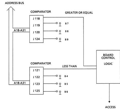
[image:12.612.50.533.309.712.2]3.2 Access to the DRAM-E3Ml Board
Easy access address and address modifier code selection
DRAM-E3Ml board is provided through jumperfields. The
address is jumper selectable in 256K byte steps to
contiguous memory configuration to other VME/P10l4 bus
boards.
3.2.1 The Access Address Selection of the DRAM-E3Ml Board
to the
access allow
based
This chapter describes the address selection of the DRAM-E3Ml
board excluding slave boards (DRAM-E3SX) because the access
address selection of the board including the slave boards is
described in chapter 4.1. The memory capacity of the DRAM-E3Ml
board is 1M byte.
The comparator Ies Jll8 to J125 decode the address range out of
the whole range of 16M byte (A24 mode) or 4G byte (A32 mode).
The least significant address signal which can be modified is A18.
A24 decoding:
23 22 21 20
y y y y
y
=
set to logical 0 or 1x
=
don't care19 18 17 16
y y x x
To allow a flexible lay-out, the DRAM-E3Ml board allows the access
address selection in 256K byte boundaries by jumper settings in
jumper areas (3 jumperfields each).
One jumper area defines the start address at which the board can
be accessed.
The other jumper area defines the first address at which the board
cannot be accessed. The address range at which the board responds
to is set by default from $FF10 0000 to $FFlF FFFF.
In a standard environment (68000 or 68010 processor) the address
lines A24 to A31 are not driven (A24 mode). The decoding logic of
the DRAM-E3Ml board provides the A32 mode and offers a full 32 bit
decoding. For this purpose the address lines A24 to A31 are
decoded every time. In an A24 environment, the upper address
lines A24 to A31 have to be ignored from the decoding logic. This
is provided through internal pull-up resistor networks which pull
the upper address lines to high state. This results in the need
to jumper the start address to $FF10 0000 for parallel decoding in the A24 and A32 mode.
Figure 3 outlines the decoding logic in a general block
and Table 2 lists the relation between the jumperfields
address range to be selected.
diagram
and the
Jumperfields B4, B5 and B6 define the start address because B7, B8
and B9 define the first address which is not on the DRAM-E3Ml.
Figure 4 outlines the location diagram of the access address
selection jumperfields.
Figure 3: The Decoding Logic Block Diagram
ADDRESS BUS
/
t"-COMPARATOR GREATER OR EQUAL
J 118
J 119
-y
87A 18-A31 - 0 88
J 120 ..L
J124
=-y
89BOARD CONTROL
COMPARATOR LOGIC
LESS THAN J 121
J 122
-y
84A18-A31 J 123 ~y 85
J 125 ~y 86
+
ACCESS [image:15.617.48.543.79.528.2]13 12 II 10 9 8
... 1 0\ b 5 'I 3 2
X PRESS F1NISIIIirIIIH IlUEHCHEH IIRfllH3IIIl REV. 2 CIIII'ONENTOR. 8f11JTEILSEITE
~ JI'II1 lrII
~
tiT, til
n
~
I
JI2911
JI'13~
J98~
JIOSj
th.J
~Dl£D2
suBlbBl3B15 B22;s23
Blnl2~
1~1b¥t-
m
~
... J3b~
J21til
JIB. " . '....~
J
Q
JJ5 J2b~
~_
_ JB1 . . - _ - " "
~
!3
T3lE
i
an
','flU\]}
""~
Jl'l~.
J2S~
Jib~
R1
c~1
~J~
I
JJJ J2'i JIS JbJ
.---..no<'"T'l I yR3
I
)
13314
JllfljIn
)1'191 1 yR2-U
L-.J - - - I R I Cl1
£t
""~
m11
~
lI'11
r -- - r nJ1ij2
""'\, JJI
til
J22tI
JIJtI
J'I1
Jg
I !ffJ II qrn
I
)132j
I
JB3j
I
lMl j
I
JB2j
I
JJDt1
J21t1
JI2tJ
JJj
J2JI'" JS
'1
JJ2
111
JI'II
~'{]:.
~
J2D~
JIl~
.J2~
"., , .. , ,on'
"Rl
'fi ... ..
:
L - -_ _
-"c~-..~g
I
.I91jI
JIIIt1J----
_:JlIij
JI9 Jill JI~I ~~
hKj~~ ]:,~ JI"~2:'
I
J::~~
]j
:~
JlW
~k
11
M , , 'Rill . u :9L 9 B2 C'IB
_____ Jll11--1j
I
.190 jI
11
I
Y
Cb2 DCSJ . - 4
Iij I'Xj
...
...
()) I.Q III c::
en 1'1
()) ())
en ~
()) ())
~
t-t0
"0 ()
()) III
::l rt 0- 1-"
...
0~ ::l
() tJ
...
HI III
·0 I.Q
1'1 1'1
III rt S
::T ()) 0
HI
()
0 rt
S ::T
"0 ())
...
()) ~
rt ()
()) ()
())
... en
0 en
()
III ~
rt
0-...
0-0 1'1::l ())
en
0- en
1-'.
III (J)
I.Q ())
1'1 ...
III ())
S ()
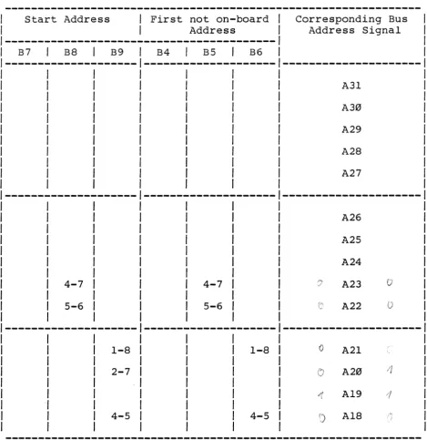
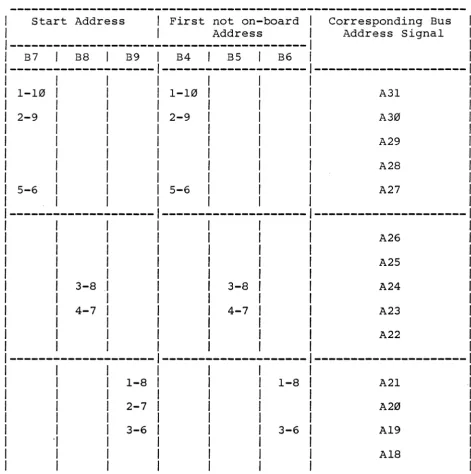
Table 2: Jumperfie1d Assignment to Access Address Selection
START Address Selection
1 Selection of 1st Inot on-board Addr
Jumperfie1d Corresponding Jumperfie1d
Bus Address Signal
. B7 1 B8 1 B9 B4 1 B5 1 B6
1 1
1-101 A31 1-101
1 1
2-9 1 A30 2-9 1
1 1
3-8 1 A29 3-8 1
1 1
4-7 1 A28 4-7 1
1 1
5-6 1 A27 5-6 1
1 1
1 1
1-101 A26 1-101
1 1
2-9 1 A25 2-9 1
1 1
3-8 1 A24 3-8 1
1 1
4-7 1 A23 4-7 1
1 1
5-6 1 A22 5-6 1
1 1
1-8 A21 1-8
2-7 A20 2-7
3-6 A19 3-6
4-5 A18 4-5
[image:17.617.66.547.67.586.2]Table 3: Default Access Address Selection
Start Address 1 First not on-board I Corresponding Bus I
I Address I Address Signal I
1---1
11 B7 1 B8 1 B9 1 B4 1 B5 I B6 1 1
1---1---1---1
1 I 1 1 1 I I I
1 I 1 1 1 I A31 I
1 1 1 1 I 1 I
I I 1 1 1 I A30 1
1 I 1 1 I 1 1
1 1 1 1 1 1 A29 I
I I I 1 I I 1
I 1 1 I I I A28 I
1 1 1 I I I 1
I 1 I I I 1 A27 I
1 I 1 I I I I
---1---1---1
I 1 1 1 1 1 1
1 1 1 1 1 I A26 1
I 1 1 1 1 I I
1 1 1 1 1 1 A25 1
1 1 1 1 1 1 I
I 1 1 1 1 1 A24
1 I 1 1 I 1
I 4-7 1 1 1 4-7 1 1 A23
o
1 1 1 I 1 I
1 5-6 1 I 1 5-6 1 1 A22
1 1 1 1 1 1
---1---1---1 I 1 1 1 1
1 1 1-8 1 1 1 1 A21
1 1 1 1 1 1
1 1 1 1 1 2-7 1 A20
1 1 1 1 1 1
1 1 3-6 I 1 1 3-6 I A19
-I I 1 1 1 1
1 1 4-5 1 1 1 4-5 1 A18
I 1 1 1 1 1
A32 1 A24
--- 1---
!(;'2,
1
Start Address: $FFI0 0000 1 $10 0000
1
End Address: $FFIF FFFF 1 $IF FFFF
1
First not on-board Address: $FF20 0000 1 $20 0000
1
Boundary: $0010 0000 1 $10 0000
[image:18.618.49.547.70.599.2]3.2.2 Modification of the Access Address of the DRAM-E3Ml
Due to the full decoding of the 21 address signals, the DRAM-E3Ml
can be jumpered to react on different access address ranges.
Tables 4, 5 and 6 outline 3 examples of the DRAM-E3Ml
configuration for different memory ranges.
To adapt the board access address range to the appropriate range,
please follow the following rules:
1) Calculate the start address of the board and list the address
line value A3l to AlB in binary form (0 or 1)
2) Calculate the first not on-board address by adding the boundary
and list the address line value A3l to AlB in binary form
(0 or 1)
·3) Install or remove the jumpers in the jumperfields B4 to B9 in
the following way:
a 0 on the corresponding address signal is equivalent to an
inserted jumper,
a 1 on the corresponding address signal is equivalent to a
removed jumper.
Table 7 gives an empty form for installation of the used setup.
Note:l) If the A32 and the A24 mode is used,
A24 to A3l must be high for a valid
not, the A24 decoding is disabled.
the address signals
A24 decoding. If
2) If only the A32 mode is used, there are no limitations
regarding address selection.
3a) If only the A24 mode is used, A24 to A3l must be high
(provided through on-board pull-up register networks) if
not disabled (see 3b).
3b) If only the A24 mode is used, A24 to A3l can be disabled
by removing the jumper at jumperfield BIB.
Caution: In the default configuration BIB is not inserted (A24 mode is enabled!)
Table 4: Access Address Selection Example 1
I Start Address 1 First not on-board 1 Corresponding Bus
1 1 Address 1 Address Signal
1---1
I B7 I B8 1 B9 1 B4 1 B5 1 B6 1
1---1---1---I I 1 1 1 1
I 1 1 1 1 1 A31
1 1 I I 1 1
1 1 I I 1 I A30
1 1 1 1 I I
I I I 1 1 1 A29
1 1 I 1 1 I
1 I 1 I 1 1 A28
I 1 1 1 I I
I I I 1 I 1 A27 1
1 1 1 1 1 1 1
---1---1---I I 1 1 1 1
1 I I I I 1 A26
1 1 1 1 1
1 1 1 1 1 A25
1 1 1 I
1 1 1 I A24
1 1 1 1
1 4-7 1 1 4-7 1 A23
1 1 1 I
1 5-6 1 1 5-6 1 A22
1 1 I 1
I
I
1
1 1 1 1 1 1
1-8
2-7
4-5
1-8
4-5
A21
A20
A19
A18
A32 A24
---1---Start Address: $FF08 0000 $08 0000
End Address: $FF17 FFFF $17 FFFF
First not on-board Address: $FF18 0000 $18 0000
[image:20.618.52.521.61.543.2]Table 5: Access Address Selection Example 2
1 Start Address 1 First not on-board Corresponding Bus
1 1 Address Address Signal
1---1 B7 1 B8 I B9 B4 1 B5 1 B6
1--- ---
---1 1 1 1
1 1 1 1 A31
1 1 1 1
1 1 1 1 A30
I I 1 1
1 1 1 A29
1 1 1
1 1 1 A28
1 1 1
1 1 1 1 A27
1 1 1 1 1
---
---1---1 1 1 1
1 1 1 1 A26
1 1 1 1
1 1 1 1 A25 1
1 1 1 1 . 1
1 1 1 1 A24 1
1 1 1 1 1
1 4-7 1 4-7 1 1 A23 1
1 1 1 1 1
1 1 1 1 1 1 A22 1
1 1 1 1 1 1 1
---1---1---1
1 1 1 1 1 1 1
1 1 1 1 1 1 .. i A21 1
1 1 1 1 1 1 1
1 1 2-7 1 1 1 1 A20 1
1 1 1 1 1 1 1
1 1 3-6 1 1 1 3-6 I A19 1
1 1 1 1 1 I 1
1 1 1 1 1 1 A18 1
1 1 1 1 1 I 1
A32 A24
---
---Start Address: $FF64 0000 $64 0000
End Address: $FF73 FFFF $73 FFFF
First not on-board Address: $FF74 0000 $74 0000
Boundary: $0010 0000 $10 0000
1M byte 1M byte
[image:21.621.68.548.64.544.2]Table 6: Access Address Selection Example 3
Start Address
I
First not on-boardI
Address1---B7 B8
I
B9 B4I
B5I
B6Corresponding Bus Address Signal
--- --- ---1
I
1-10
I
1-10I
2-9
I
2-9I
1
I
1
I
5-6
I
5-61 A31 A30 A29 A28 A27
---
---J---11 A26
1
I
A251
3-8
I
3-8 A241
4-7
I
4-7 A23I
1 A22
1
--- --- ---1
1 1 1 1 1 1 "I 1 1 1-8 2-7 3-6
1-8 A21
A20
3-6 A19
A18
---~---Start Address:
End Address:
First not on-board Address:
Boundary:
A32 A24
$3644 0000
$3653 FFFF
$3654 0000
$0010 0000
[image:22.617.45.517.63.537.2]Table 7: Access Address Selection
Start Address
B7
I
B8 B9---I
I
I
I
I
I
I
I
I
I
I
I
I
I
I
I
I
I
I
I
I
I
---I
I
I
I
I
I
I
I
I
Start Address:
End Address:
I
First not on-boardI
AddressB4 B5
I
B6Corresponding Bus Address Signal
---
---I
I
A31I
I
A30I
I
A29I
I
A28I
I
A27I
I
I
A26I
I
A25I
I
A24I
I
A23I
I
A22I
---
---I
I
A2lI
I
A20I
I
Al9I
I
Al8I
A32 A24
First not on-board Address:
$ $ $ $ $ $ $ $ Boundary:
1M byte 1M byte
[image:23.620.67.549.63.561.2]3.3 The Address Modifier Decoding
The VME/P1014 specification defines address modifier (AM-) codes
which are decoded in parallel to the address signals. The 6 AM
Code signals are routed directly into a PAL and a total number of
10 different codes can be separately enabled via jumper settings.
Table 8 lists the AM-Codes which are defined in the VME/P1014
specification.
A short I/O access to the DRAM-E3M is not necessary because the
memory range of the board is greater than the range for this
AM-Code.
Additionally, the block transfer is not supported through the
DRAM-E3Ml board. Therefore, the AM codes, listed in Table 9 are
allowed. To enable each of the AM-Codes separately, the
jumperfields B2, B3 and B21 are installed on the board. Figure 5
tv 111 \J 12 \I to 9 8 7 b 5 4 J 2
o
X PRESS r1NISH GMBH MUENCHEN ORAM-E3MO REV. 2 COMPONENTOR. BAUTEILSEITE ttl I-'
CD
§
~ rnCD
-'I
JI29~
JI43~
J99~
JIOSj!(]
D t : 1JI51
r
n n -mlIj
rn
CD CD
~
CDP 0. 1-" >< ()
U
~
t'tl~
'1
!;=II ill
L~h
_[
l{_73 _ _ ----'1
JI53jO:I
R3~~
Iw
J3b J21 JI9 J9
J35 JI1 J9
J34 JIb J1
JJ3 JI5 Jb
I-tt 0 11 rt ::r' CD 0 0 S "0
I
~
JI49 LJ :§:~
1
JIJJ1j Jlqqjrl:::1
rl:::1
rH9 1 J I ~!J (71
I
J32ii
J23 i"{ J14"hi JS9
~
JI41id
]7711
J791I
J91,1
Jlq21~
J31~I
J22il
JIJ~I
J4[tJ1
uJI"11
COl ,
lion!,
1 I
112;:
""
M
J1I
~
JI2
~. J3~
w I-' CD rt CD I-' 0 0 ~ I~ J2
BIoi
"I
l o nl 9" [ { ] ;J29]1
""]I
JII,..--_ _ n-;----",.,-,
JQq
ca
]854I
,''01J
JJ
I
JI9J
I
JIO JIrt 1-" 0 P 0. 1-" ~ to 11 ~ S
.
1f2 Icr xg
I
J::~ JI~ ~~~
J:
1~ Jl3~2:
1
IJ123~
:~
: : 1 •JID~
•JI,"~
JI:Jb,
1"J
JlZ
~I 7:'~
I
Jlm1?.~
' - -_ _ ----'J,!.!.lwts ChD
JI"
ml
JlI9@t~.1c~ ~c~\--
w" _ _"j(
~
D 1
,~
: ; ; ' RSl~
~ yffi2 '
I
j
Mjab
fPYfTTfF"""""""""""""""""""""""""""""""""",'"""""""""""""""""1""""'1""""'1""""'1""""'1"""'"1""""'1""""
o
1 2 J 4 5 b 1 9 9 10 II 12 IJ 14 15 Ib 11 19Table 8: The Address Modifier Codes
---I
HEX 1 Address Modifier 1 Function 1I CODE 1 5 4 3 2 1 0 1 1
1---1
I
1 1I
1 3F 1 H H H H H H 1 Standard Supervisory Block Transfer 1
/ 3E / H H H H H L 1 Standard Supervisory Program Access 1
/ 3D / H H H H L H 1 Standard Supervisory Data Access 1
1 3C 1 H H H H L L / Reserved
I
1 3B 1 H H H L H H 1 Standard Non-Privileged Block Transfer/
1 3A 1 H H H L H L 1 Standard Non-Privileged Program Access 1
1 39 1 H H H L L H / Standard Non-Privileged Data Access 1
1 38 1 H H H L L L 1 Reserved 1
I
1 1 11----1---1---1
1 1 1 1
1 37 1 H H L H H H 1 Reserved
I
1 36 1 H H L H H L 1 Reserved 1
1 35 1 H H L H L H 1 Reserved 1
1 34 1 H H L H L L 1 Reserved 1
1 33 1 H H L L H H
I
ReservedI
1 32 1 H H L L H L 1 Reserved 1
1 31 1 H H L L L H 1 Reserved 1
1 30 1 H H L L L L 1 Reserved 1
1 1 1
I
1----1---/---1
1 1 1 1 1 11 1
2F 1 H L H H H H 1 Reserved
2E 1 H L H H H L 1 Reserved
2D 1 H L H H L H 1 Short Supervisory Access
2C 1 H L H H L L
I
Reserved2B 1 H L H L H H
I
Reserved2A
I
H L H L H L 1 Reserved29 1 H L H L L H
I
Short Non-Privileged Access28
I
H L H L L L 1 ReservedI
-~---I---27 H L L H H H Reserved
26 H L L H H L Reserved
25 H L L H L H Reserved
24 H L L H L L Reserved
23 H L L L H H Reserved
22 H L L L H L Reserved
21 H L L L L H Reserved
20 H L L L L L Reserved
---L = low signal level
H
=
high signal level [image:26.618.47.522.55.638.2]Table 8 cont'd
HEX
I
Address ModifierI
FunctionCODE
I
5 4 3 2 1 0I
IF
IE lD Ie lB lA 19 18 17 16 15 14 13 12 11 10L H L H L H
L H
L H
L H
L H L H
H H H
H H H
H H L H H L
H L H H L H
H L L
H L L
L H L L H L L H L L H L L H L L H L
L H L
L H L
H H H H H L H L L H L H
L L
L L
H L H L H L H L H L H L H L H L
User defined User defined User defined User defined User defined User defined User defined User defined
User defined User defined User defined User defined User defined User defined User defined User defined
1---- ---
---0F 0E 0D 0e 0B 0A 09 08 07 06 05 04 03 02 01 00
L L
L L
L L L L L L
L L
L L
L L
L L
L L L L
L L
L L
L L
L L
L L
H H H H H H
H H L H H L H L H H L H H L L H L L
L H H
L H H L H L L H L
L L H
L L H
L L L
L L L
H L H L H L H L H L H L H L H L
Extended Supervisory Block Transfer Extended Supervisory Program Access Extended Supervisory Data Access Reserved
Extended Non-Privileged Block Transfer Extended Non-Privileged Program Access Extended Non-Privileged Data Access Reserved Reserved Reserved Reserved Reserved Reserved Reserved Reserved Reserved
L
=
low signal levelH
=
high signal level [image:27.617.68.545.64.631.2]Table 9 lists the selectable AM-Codes.
Table 9: The AM-Code Selection
I Jumperfield / HEX 1 1
/---1
CodeI
FunctionI
1 B2 I B3 / 1 I
/---1
I
I
/
I
I
1 1-16 I I 3E I Standard Supervisor Program Access 1
I I 1 1 1
1 2-15 I 3D 1 Standard Supervisor Data Access I
1 1 1 1
1 3-14 I 3A 1 Standard Non-Privileged Program Access 1
1 1 I 1
I 4-13 1 39 Standard Non-Privileged Data Access 1
1 1 1
1--- ---1--- ---1
1 1 1
1 5-12 1 0E Extended Supervisor Program Access 1
I / 1
1 6-11 1 0D Extended Supervisor Data Access I
1 1 1
1 7-10 1 0A Extended Non-Privileged Program Access 1
1 1 I
1 8-9 I 09 Extended Non-Privileged Data Access I
1 1 1
/--- ---1--- ---1
1 / 1
1 1-10 1 10 USER defined 1
1 1 1
/ 3-8 1 11 USER defined 1
1 / 1
1 4-7 1 * 1
/ 1 1
1 5-6 1
*
11
'I
/
/
1
/---1---/---1---1
/ / / 1 /
/ / 2-9 / / Respond always
*
11 / / 1 /
*
for test purposes only. [image:28.615.64.521.98.582.2]Each of the AM-Codes may be used in the environment. To enable an AM-Code, the corresponding connection has to be provided.
Table 10 lists the default condition during manufacturing. If the
default set-up is not usable and a special set-up has to made,
please follow the following 2 rules:
1) Define the AM-Codes for the DRAM-E3Ml board.
2) Insert or remove the jumpers in jumperfield B2 and/or install
or remove a wire on the jumperfield B3 in the following way:
An inserted jumper/wire enables the corresponding AM-Code (as
listed in Table 9) because a removed jumper/wire will disable
the corresponding AM-Code.
Tables 11 to 13 list examples for AM-Code combinations. is an empty form.
29
Table 10: Default AM-Code Selection
X
Jurnperfield Connections
1---1
I
B2I
B3AM-Code Enabled
AM-Code (x)
1---1
1-16
2-15
3-14
4-13
1---5-12
6-11
7-10
8-9
3E
3D
3A
39
I
I
I
I
I
I
I
I
I
y
y y
y
---1---0E
0D
0A
09
I
I
I
I
I
I
I
I
I
y y y
y
--- --- ---J---I
10 N
[image:30.617.48.518.67.436.2]Table 11: AM-Code Selection Example 1
Jumperfield Connections AM-Code 1 Enabled
1---1
1 AM-Code (x)I B2 1 B3 1 1 1
1---1
1 1 1
1 1-16 1 3E Y 1
1 1 1
2-15
I
3D YI
1 1
1 3A N I
1 I
1 39 N 1
I 1
--- ---1--- ---1
1 1
5-12 1 0E Y I
1 1
6-11 I 0D Y 1
I 1
1 0A N 1
1 1
I
09I
NI
1 1 I 1
1--- ---1---1---1
I 1 1 1
1 1 10 1 N 1
I
I
1
I
1 1 11 1 N 1
1 1 1 1
Example 1: The DRAM-E3Ml responds to 24 bit and 32 bit addressing
(A24 and A32 mode) only under Supervisor mode. All
non-privileged accesses are ignored.
[image:31.618.63.538.63.445.2]Table 12: AM-Code Selection Example 2
I
Jumperfield Connections
---1
B2 B3
AM-Code Enabled
AM-Code (x)
---1
1-16 3E Y
2-15 3D Y
3-14 3A Y
4-13 39 Y
0E N
0D N
0A N
09 N
1---I
I
I
I
I
10
11
N
N
Example 2: All A32 mode accesses are. ignored by the DRAM-E3Ml
[image:32.617.48.519.65.441.2]Table 13: AM-Code Selection Example 3
Jumperfield Connections AM-Code Enabled 1
---1
1 AM-Code (x) 1B2 1 B3 1 1 1
---1
1 1 1
1 1 3E N 1
1 1 1
1 1 3D N 1
1 1 1
1 1 3A N 1
1 1 1
1 1 39 N 1
1 1 1
---1---1--- ---1
1 1 1
5-12 1 1 0E Y 1
1 1
6-11 1 0D Y 1
1 1
7-10 1 0A Y 1
1 1
1 8-9 1 09 1 Y I
1 1 1 1
1---1--- ---1---1
1 1 1 1
1 1 1-10 10 1 Y 1
1 1 1 1
1 1 3-8 I l l y 1
1 1 1 1
Example 3: A32 mode accesses as well as the user defined AM-Codes
10 and 11 are supported. All other AM-Codes (i.e. the
A24 mode) are ignored.
[image:33.618.68.540.68.437.2]Table 14: AM-Code Selection
Jurnperfield Connection AM-Code 1 Enabled
1---1
1 AM-Code (x)I B2 1 B3 I 1
1---1 I 1 I
1 1 1 3E 1
I 1 1 1
1 1 1 3D 1
1 1 I 1
1 1 3A 1
1 1 I
1 1 39 1
1 1 1
1---
---1---1---1 I 1
1 I 0E I
I
I
I
I
I
0DI
I
I
I
1 1 0A 1
1 1 1
I 1 09 1
1 1 1 1
1---1---1---1---1 1 1 1
1 1 1 10 1
1 1 1 1
1 1 1 11 1
[image:34.615.48.511.64.432.2]3.4 The Parity Check
The DRAM-E3Ml board contains 36 memory chips (256K * 1 bit): 32
bits for data storage and 4 bits for byte parity information.
The board supports 8, 16, 24 and 32 bit data transfers. Each of
the 4 bytes which may be read or written at the same time, has a
separately controlled parity checker/generator.
The parity generator is activated on every write access only for
the selected bytes (up to 4) which are transferred.
On read accesses the parity checker for the selected byte(s) is
activated by default during manufacturing.
If a parity error is detected and if the parity check is enabled,
the DRAM-E3Ml board drives the BERR signal instead of the DTACK*
signal. On occurrence of a parity error, the red FAIL LED on the
front panel lights up.
The byte parity check can easily be disabled by following the
rules listed below:
1) Remove jumper at jumperfield B20
2) Remove jumper between pin 2 and pin 5 at jumperfield B14
3) Install a jumper between pin 1 and pin 6 at jumperfield B14.
The default connections during manufacturing for the enabled parity check are listed below:
Table 15: Parity Check Jumper Fields
B20 B14 Mode
I
Note1---1
1 1
1 IN 1 2 - 5 I Parity Error Check enabled 1
*
11 1 1 1 1
1---1---1---1---1
1 1 I 1 1
lOUT 1 1 - 6 1 Parity Error Check Disabled 1 1
1 1 1 1 1
*
Default conditionFigure 6 outlines the location diagram of the parity check
[image:36.617.51.495.117.237.2]Figure 6: Parity Check Jumperfield Locations
Please see Appendix C for the complete location diagram.
N
~DI ~J~I1L3 ______ ~!~J~llill ______ ~~~ ______ ~~~ ______ ~~~JlWlb~ ______ ~rft~
JI17
N
=; =;
NoD
IJ"~
I (U
'is
a:;p-Iir
~
,..
r
~p::::
::;
en
CD
I - -
:r-P-B I - -r '
-C'l'l
:r
~
~::;
'"
CD_
;n
N NCD a::
~
~'
-=~
_ Ne~
I;
a:: N::;
1:51
CD ;!:;
[)
c
::; ::;
Cl
oD
'-'
C'iD
~ bJI~
D
M~
Lf>en ~...,w
3
~
~6
i
~ B 3 0CD
OC31
[E
--c5IJ ~
f-'§ ~
..., ::;
~
' - - '
[image:37.618.67.565.78.742.2]3.5 The Access Times
The DRAM-E3Ml board is a high speed dynamic RAM board which
provides the following access times:
Table 16: Access Times of the DRAM-E3Ml
I
Access TimesI
Type1
Max1
1---J
/ 1
WRITE with Parity Generation 70ns / 80ns 1
/ . I 1 1
/---1---1---I
1 / 1 /
/ READ with Parity Check / 24Sns / 26Sns 1
/ 1 / /
/ READ without Parity Check / 210ns / 22Sns /
/
1
1
1
The access time is measured from the falling edge of one of the
two data strobes to the falling edge of DTACK* generated from the
DRAM-E3Ml board.
The cycle time from the beginning of a cycle is 31Sns typ / 335ns
max.
Due to the interleave structure of the board (decoding and next
access are interleaved), a high throughput is provided. If an
access was forced, the next access can occur within the following
time frames:
Next ACgess after TYP AAX
---WRITE
R~D
Therefore, the
VME/P1014 bus
timing).
250ns 270ns
70ns 90ns
following transfer capacity is provided on the
{if the transfer device has an ideal VME/P1014
Cycle / TYP MIN
---WRITE
R~D
/
1
/
1
/
12.0M byte/s/
/
12.0M byte/sl
11.0M byte/s
[image:38.617.48.457.146.296.2]3.6 The Refresh
The refresh for the dynamic RAMs is distributed over 4ms and
provision is made to minimize the overhead and delay to the VMEbus accesses.
After the internal read cycle of the DRAMs is finished and the
data on a read cycle has been stored in the output data latches, a
pending refresh request (every l5us) is executed independent from
all VMEbus activities. Therefore, the overhead time for the
VMEbus protocol is used to refresh the RAMs. In addition to the
refresh interleave, a refresh to the DRAMs is forced if a not
on-board access is detected between 11 and l5us after the execution
of the last refresh.
A 68010 processor with a clock frequency of l0MHz can access the
DRAM-E3Ml board without extra wait states for the DRAM refresh if
the used program runs on the DRAM-E3Ml or DRAM-E3SX.
The refresh control logic for the FMEbus slave modules (memory
expansion) is included on the DRAM-E3Ml board.
TYP MAX
Overhead time for refresh
I
l20nsI
450nsAn access can stay for a longer time than the refresh period
(15us) because every access cycle on the board is aborted if the
correct data is stored on the RAMs or in the output latches to the VMEbus.
Therefore, correct refresh is provided if a system hang-up occurs
or if a bus master holds an access for a long time.
If the board is jumpered to work from the standby power, refresh
for the dynamic RAMs is provided during main power down.
3.7 The Battery Backup Option
The DRAM-E3M1 board can be powered from the +SV main power or from the +SVBAT pins of P2 connector (SA-30/31/32).
The default condition during manufacturing is the connection to
the +SV Main Power.
Table 17 lists the jumper settings which have to be made for the
different modes, and Figure 7 outlines the location diagram of the jumperfields.
Table 17: The Battery Backup Option
I
OptionI
B11J---I
I
Battery BackupI
I
I
I
5-10 6-9 7-8
1---1---I
I
I
5V STDBY (optional)I
I
I
4-111---1---
.
I
I
I
+5V MAINI
I
I
[image:40.617.51.313.186.398.2]Figure 7: Location Diagram of the Battery Backup Jumperfields
Please see Appendix C for the complete location diagram.
DC31
[image:41.620.70.550.69.737.2]3.8 The Front Panel
The DRAM-E3Ml board contains a RUN/LOCAL switch which disables the
board from the VME/P10l4 bus if set to LOCAL. In RUN position,
the green "RUN" LED on the front panel turns on, and the red
"FAIL" LED lights up if the board is in LOCAL mode.
During normal operation the "FAIL" LED may turn on if a parity
error is detected. The parity error is latched and only reset if
the board is reset through the SYSRESET* signal from the VMEbus or through a RUN-LOCAL-RUN change of the RUN/LOCAL switch.
Additionally, a yellow SELect LED is installed. The LED turns on
if the board is selected (an access is pending).
Figure 8 shows the front panel lay-out in detail.
I RUN I FAIL I Function 1
1---1
1 1 1 1
1 1 X 1 Board in LOCAL mode 1
1 1 I 1
I X I I Board in RUN mode 1
1 I 1 1
1 X I X I Board in FAIL mode 1
1 I I 1
Note: All other combinations are not possible.
Figure 8: The Front Panel of the SYS68K/DRAM-E3Ml
D
o
RUN@
R/Lo
FAILo
SELD
43
RUN LED
RUN/HALT SWITCH
FAIL LED
[image:43.615.232.512.72.732.2]4.0 The FMEbus Interface
The DRAM-E3Ml board contains an FMEbus interface for memory
expansion. All the control logic for access and refresh is
included on the DRAM-E3Ml board to allow cost effective memory
expansions.
The general block diagram of the FME concept is shown in Figure 9.
Cost and space intensive ICs are spent only on the master
interface (DRAM-E3Ml) and only driver circuitries are included on
the DRAM-E3SX boards. This allows easy memory expansion through 1
or 2 slave boards.
The following slave boards are now available to interconnect the
DRAM-E3Ml:
Board
DRAM-E3S1 DRAM-E3S3 DRAM-E3S6
Capacity
IMbyte 3Mbyte 6Mbyte
A maximum of 13M byte DRAM is provided using a DRAM-E3Ml and two
DRAM-E3S6 boards.
Easy installation of the slave boards is provided through the 3rd
Figure 9: The FME Concept
SYS68K1DRAM-E3M 1 SYS68K1DRAM-E3S (1 ,3,6) SYS68K1DRAM-E3S (1,3,6)
<
FME BUS (~2 Bitl;
;
;
FMEBUS FMEBUS FMEBUS
DRAM
CHIPS PARITY CHECK PARITY CHECK PARITY CHECK
(36) CONTROL
DRAM DRAM
LOGIC CHIPS CHIPS
(max216) (max216)
VME BUS INTERFACE
~
r;,-)
~
r;,-)
~
r;,-)
;
;
..
< VME BUS '1613:' Bit)
..
>
1MB
7MB
13MB I.
[image:45.620.73.561.114.332.2]The connection as a second slave board requires a fulfilled first
slave board (boards may be exchanged in order of position).
Please follow the installation rules in the DRAM-E3SX manual.
Table 18: Usable Slave Board Combinations
1st Slave 2nd Slave
I
Total Memory CapacityE3Ml 1M byte
E3Ml E3Sl 2M byte
E3Ml E3S3 4M byte
E3Ml E3S3 E3Sl 5M byte
E3Ml E3S3 E3S3 7M byte
E3Ml E3S6 7M byte
E3Ml E3S6 E3Sl 8M byte
E3Ml E3S6 E3S3 10M byte
E3Ml E3S6 E3S6 13M byte
[image:46.613.50.528.133.362.2]Figure 10: Block Diagram of the SYS68K/DRAM-E3S6
f\~ f\
yyy
Control
..
..
..
..
I Parity 0 Parity 1 Parity 2 Parity 3 I
p I I PARI YB
A I I
c R
I 1?
J
1?
I A\?- I A\ ~0 I
N T DATABU)
T Y 0
I
..t}
I
..t}
I
..t}
I
..t:.
~ :.R
+ A ~~
0 E T Byte 0 Byte 1 Byte 2 Byte 3 4 Parity Bits
L R A
r¥
R
~
~
I I I I I I I I I I I I I I IB
0 B
U R U rV
W\
s s Byte 0 Byte 1 Byte 2 Byte 3 4 Parity Bits
B A
___ hi
u D I I I I I I I I I I I I I I I
, s :.
,
:. D ~W\R
Byte 0 Byte 1 Byte 2 Byte 3 4 Parity Bits
E
:'"
~
[1
FME I I I I I I I I I I I I I I I
BUS BrV
W\
I<~
___
hi
Byte 0 Byte' Byte 2 Byte 3 4 Parity B.tsINTERFACE
I I I I I I I I I I I I I II
P3 ~W\
Byte 0 Byte 1 Byte 2 Byte 3 4 Parity Bits
L-'\
~
r¥
J U J I I I I I I I I I I IrV
W\
Byte 0 Byte 1 Byte 2 Byte 3 4 Parity Bits
,A. ~hI
I
I
I
I:
I
DECODING \ ;
-LOGIC BYTE DN- RDL
VMEBUSP2 I I VME BUS P1
[image:47.617.66.560.91.488.2]4.1 Access Address Selection using FME Slave Boards
Due to the fact that the memory capacity is expanded using
DRAM-E3SX boards (see Table 18), the access address selection has to be
changed. The general calculation rules, outlined in chapter
3.2.2, are usable to reconfigure the default setup of the board.
The default access address selection of each DRAM-E3Ml board is
outlined in chapter 3.2.1.
Table 19 lists the extension of the default access address
selection using a DRAM-E3S1 board. Table 20 lists the extension
using a DRAM-E3S3 board while Table 21 lists the extension with a
DRAM-E3S6 board. All other modifications are similar to the
Table 19: Access Address Selection using one DRAM-E3S1
Start Address
B7 1 B8 B9
---1 1 1 1
I
1 1I
I
I
I
I
I
1I
I
1 11 4-7
1
1 5-6
1
---1
1 1-8
1 1
1
I
3-61
1 4-5
1
Start Address:
End Address:
I
First not on-board Corresponding BusAddress Signal
1 Address
B4 B5 B6
A31 A30 A29 A28 A27 A26 A25 A24
4-7 A23
5-6 A22
A21
A20
3-6 A19
4-5 A18
A32 1 A24
---1---1
$FF10 0000
I
$10 00001
$FF2F FFFF 1 $2F FFFF
1
First not on-board Address: $FF30 0000
I
$30 0000I
Boundary: $0020 0000
I
$20 0000I
2M byte
I
2M byte [image:49.620.66.547.64.545.2]Table 20: Access Address Selection using one DRAM-E3S3
i
Start Address 1 First not on-board 1 Corresponding BusI 1 Address 1 Address Signal
1---1
11 B7 1 B8 1 B9 1 B4 1 B5 1 B6 1 1
1---1---1---1
1 1 1 1 1 1 1 1
1 1 1 1 1 1 1 A3l 1
1 1 1 1 1 1 1 1
1 1 1 I I 1 1 A30 1
1 1 1 1 1 1 1
1 1 1 1 1 1 A29 1
1 1 1 1 1 1 I
1 1 1 1 1 1 A28 1
1 1 I 1 I 1 1
1 1 1 1 1 1 A27 1
1 1 1 1 1 1 1
1--- ---1---1
1 1 1 I 1 I 1
I 1 1 1 1 I A26 I
I 1 1 1 1 1
1 1 1 1 1 A25 1
1 I 1 1 1 1
1 1 1 1 1 A24 1
1 1 1 1 1 1
I 4-7 1 1 4-7 1 1 A23 1
1 1 I I 1 I
I 5-6 1 I I I 1 A22 1
I 1 I I 1 1 1
---I---I----~---1
1 1 1 1 1 1 1
I 1 1-8 1 1 I 1-8 1 A21 1
1 1 I 1 1 1 1
1 1 1 1 1 1 A20 1
1 1 1 1 1 I I
1 1 3-6 1 I 1 3-6 I A19 1
'I 1 I 1 1 I 1
I 1 4-5 1 1 I 4-5 I A18 I
1 I 1 1 I 1 1
A32 1 A24
---1---I
Start Address: $FF10 0000 1 $10 0000
1
End Address: $FF4F FFFF
I
$4F FFFF1
First not on-board Address: $FF50 0000 1 $50 0000
I
Boundary: $0040 0000
I
$40 0000 [image:50.618.48.517.72.659.2]Table 21: Access Address Selection using one DRAM-E3S6
Start Address
I
First not on-boardI
AddressCorresponding Bus Address Signal
B7 B8 B9 B4 B5
I
I
I
I
I
I
I
4-7
I
I
5-6 5-6
I
I
I
I
B6
1---1---1-8 1-8
2-7
3-6 3-6
4-5 4-5
A32
---Start Address: $FF10 0000
End Address: $FF7F FFFF
First not on-board Address: $FF80 0000
Boundary: $0070 0000
7M byte
51
A3l
A30
A29
A28
A27
A26
A25
A24
A23
A22
A2l
A20
A19
A18
A24
---$10 0000
$7F FFFF
$80 0000
$70 0000
[image:51.620.62.546.67.546.2]Table 22: Access Address Selection using two DRAM-E3S6
1 Start Address 1 First not on-board 1 Corresponding Bus
1 I Address / Address Signal
/---1
/ B7
1
B8I
B9I
B4I
B5I
B6I
1---1---1---I
I
A31I
I
A30/
I
A29/
/ A28
/
I
A27I
--- --- ---1
I
I
A26I
, A25
I
, A24
I
4-7
I
A23I
5-6 , A22
I
,
1-8I
I
I
I
3-6"
,
4-5I
Start Address:
End Address:
First not on-board Address:
Boundary:
I
A21
2-7 A20
3-6 Al9
4-5 Al8
A32 A24
$FFI0 0000
$FFDF FFFF
$FFE0 0000
$00D0 0"100
[image:52.617.51.517.68.544.2]5.0 Preparation for Use
a) Please read the complete manual for easy and correct board
handling.
b) Make optical check of the multi-layer board and the components
for eventual damages prior to mounting the board.
c) Use adequate electrical outlets for check.
d) Use adequate equipment for electrical check (i.e. volt meter).
e) Use power supply with sufficient drive capacity within the
VMEbus tolerances.
f) To initialize the DRAM-E3Ml and its connected slave boards an
initialization routine has to be installed before reading from the board.
The following program example (subroutine) is useful for
. initialization:
STARTADR ENDADR
= =
START
LOOP
first on-board address last on-board address
LEA.L LEA.L MOVE.L CMPA.L BLT.S RTS
STARTADR,A0 ENDADR,Al #0, (A0)+ Al,A0 LOOP
Note: The initialization of the DRAM cells has to be done with
long-word moves.
5.1 Power On
When the board is mounted in a VMEbus environment and the power is stable, transfers to and from the board can be forced.
Caution: If the board has not been initialized, parity errors may
occur during read cycle because the data bits of the
DRAMs are not in a definite state after power up.
Normal access can be forced to the default set address ranges if
the following items are provided:
a) RUN/LOCAL switch is in RUN mode.
b) The current bus master can force an access to this board under
the default access address range and AM code.
Access Address Range: $FF100 000 Start A32 Mode
$FFIFF FFF End A32 Mode
$100 000 Start A24 Mode
$lFF FFF End A24 Mode
Selected AM Codes: 09, 0A, 0D, 0E
APPENDIX A
Specification SYS68K/DRAM-E3Ml
Capacity:
Organisation:
Data Transfer Modes:
Access Times:
Refresh:
Decoding:
Specials:
Memory Expansion:
Power Requirements:
Operating Temperature:
Storage Temperature:
Relative Humidity:
Dimensions:
1M byte dynamic RAM including Byte Parity Check
36 bit internally including 4 parity bits
A24:D8 : A24:D16 : A24:D24 : A24:D32 A32:D8 : A32:D16 : A32:D24 : A32:D32
Write: 70ns (typ) with Parity generation
Read: 245ns (typ) with Parity check
2l0ns (typ) without Parity check
Interleave every l5us
Jumper selectable Access Address in
256K byte increments and Address
Modifier Code (any combination of
10 AM codes)
Through FMEbus (up to 13M bytes)
Battery backup through P2 RUN/LOCAL switch
RUN/LOCAL & ERROR/ACCESS LEDs
+5V 5.9A (refresh
+5V 4.3A (average
+5V 3.2A (average
+5V STDBY 3.9A (refresh
+5V STDBY 1.9A (average
+5V STDBY 1.7A (average
o
to +60 degrees C-55 to +85 degrees C
0-95% (non-condensing)
Double Eurocard
233x160mm (9.2x6.3")
A-I
APPENDIX B
COMPONENT PART LIST
rcs
Location Type Manufacturer
---J1 - J36 41256-12 NEC,HIT,FUJ
J73 74F244 MOT,F,VALVO
J75 AM2966 AMD
J76 74F373 MOT,F,VALVO
J77 74F32 MOT,F,VALVO
J78 74F38 MOT,F, VALVO
J80 74F280A MOT,F,VALVO
J81 74F280A MOT,F,VALVO
J82 74F243 MOT,F,VALVO
J83 FRC 82 FORCE PAL 20L8A
J84 74F280A MOT,F,VALVO
J85 74F280A MOT,F,VALVO
J86 FRC 79 FORCE PAL 20L8A
J87 FRC 77 FORCE PAL 16L8A
J88 FRC 78 FORCE PAL 16L8A
J90 74F373 MOT,F,VALVO
J91 74F373 MOT,F,VALVO
J92 74F373 MOT,F,VALVO
J93 FRC 80 FORCE PAL 20L8A
J94 74F241 MOT,F,VALVO
J95 74F241 MOT,F,VALVO
APPENDIX B
COMPONENT PART LIST
ICs
Location Type Manufacturer
J96 74F241 MOT,F,VALVO
J97 74F241 MOT,F,VALVO
J98 74Fl12 MOT,F,VALVO
J99 74LS244 MOT,F,VALVO
Jl00 74LS393 MOT,F,VALVO
Jl05 74F74 MOT,F, VALVO
Jl06 74AS374 TI
Jl07 74AS374 TI
Jl08 74AS374 TI
Jl09 74AS374 TI
Jl10 74AS374 TI
JIll 74AS374 TI
Jl12 74F373 MOT,F,VAVLO
Jl13 74F373 MOT,F,VALVO
Jl14 74F373 MOT, F, VALVO
Jl15 74F373 MOT, F, VALVO
Jl16 74F373 MOT,F,VALVO
Jl17 74F373 MOT,F,VALVO
Jl18 74F85 MOT,F, VALVO
Jl19 74F85 MOT,F,VALVO
---APPENDIX B
COMPONENT PART LIST
ICs
Location Type Manufacturer
J120 74F85 MOT,F,VALVO
J121 74F85 MOT, F, VALVO
J122 74F85 MOT,F,VALVO
J123 74F85 MOT, F, VALVO
J124 74F85 MOT,F,VALVO
J125 74F85 MOT, F, VALVO
J126 74F04 MOT, F, VALVO
J127 74Fll MOT,F,VALVO
J128 74F20 MOT, F, VALVO
J129 74F109 MOT, F, VALVO
J130 74F109 MOT,F,VALVO
J131 74S240 TI,MOT
J132 74F240 MOT,F,VALVO
J133 74Fl12 MOT, F, VALVO
J134 DDU-7J-100 TOKO
J135 DDU-7J-200 TOKO
J136 DDU-7J-200 TOKO
J137 FRC 76 FORCE PAL 20L8A
J139 74F86 MOT,F,VALVO
J140 74F86 MOT,F,VALVO
APPENDIX B
COMPONENT PART LIST
ICs
Location
I
TypeI
ManufacturerI
---I
I
J141 74LS395 MOT, F, VALVO
I
I
J142 74F08 MOT,F,VALVO
I
J143 74F38 MOT,F,VALVO
J144 74F38 MOT,F,VALVO
J145 74F13 MOT, F, VALVO
J146 74F32 MOT, F, VALVO
J147 74F132 MOT, F, VALVO
J148 74F86 MOT, F, VALVO
J149· 74F08 MOT,F,VALVO
J151 74F11 MOT, F, VALVO
J152 74LS74AN MOT, F, VALVO
J153 74LS74AN MOT, F, VALVO
J154 74LS123 MOT,F,VALVO
J155 75LS240 MOT, F, VALVO
J156 74F283 MOT,F,VALVO
J157 74F283 MOT,F,VALVO
J158 74F38 MOT,F,VALVO
J159 TL7705 TI
J160 FRC 81 FORCE PAL 16LSA
---APPENDIX B
COMPONENT PART LIST
DIODES
1 Location 1 Type 1 Manufacturer 1
1---I
1 I 1 1
1 LDI 1 2206 1 DIALIGHT GREEN 1
1 I 1 I
1 LD2 I 2406 I DIALIGHT RED I
I 1 1 I
1 LD3 1 2306 I DIALIGHT YELLOW I
1 1 I 1
1 I I 1