A THYRISTOR-CONTROLLED
A presented for
ING TRANSFORMER
Doctor of Philosophy in Electrical Engineering in the
University of
Christchurch, New Zealand.
RGM* DUKE B Sc., BGE. ( ), M.E.
of expression; for the habit of submitting to censure and
refutation, for the art of indicating assent or dissent in
graduated terms; for the habit of regarding minute points of accuracy, for the art of assuming at a moment's notice a new intellectual posture, of ent~ring into another person's thoughts quickly; for taste, for dissemination, for mental soberness; above all, for self-knowledge.
TABLE OF
List of Illustrations List
Glossary Abstract
Acknowledgements
CHAPTER 1: INTRODUCTION
CHAPTER 2: THE PROPOSED CIRCUIT
2.1 In-Phase Boosting and Bucking 2.1.1 Operation of the
Voltage Booster 2.'.2 Operation the
Voltage Bucker
ii ii
xv
xvi
xxiv
xxv
1 5 5 6 8 2.2 Proposed Quadrature Boosting and Bucking 11 2.3 Thyristor Gate Pulse Requirements 262.3.1 Gate Pulse Requirements for Booster Circuit 2.3.2 Gate Pulse Requirements
Bucker Circuit 2.4 Use a Three-Phase
Three-Winding
CHAPTER 3
THE
3.1 Gate
3 1 1 3 1.2
3.1.2.1 3 1.2.2
3 1 2.3
UNIT
led Thyristors
3 2
CHAPTER 4 THE MATHEMATICAL MODEL 4.1 Component Representation
4.1.1 The A.C. System 4.1.2 Thyristors
4.1.3 Transformers 4.1.4 Transmission
4.2 Method Analysis
4.3 Electric Network Relationships
4.3.1 Node Segregation 4.3.2 Branch Equations
4.3.2.1 Resistive Branches 4.3.2.2 Inductive Branches
48 49 49 50 52 54 55 56 57 58 58
4.3.3 Voltage and Current Relationships 59 4.3.4 State-Space Formulation 61 4.4 Solution of Electric Network Equations 62
4.4.1 Implicit Integration of the State Vector
4.4.2 Change of State Variab Integration
4 5 Disconti
CHAPTER 5: THE COMPUTER PROG&~MME
5. 1 Data Input Equations
Network
5.1 1 Input
5.1 1.1 Data
5 1.1 2 Control Data
5 1.1.3 In Data
5 1.2
5.1 2.1 5.1.2.2 5.2 Modification
Renurnbering
Network
5.2.1 Determination of Variables for Thyristor Model
5.2.1.1 Determination of Thyristor Currents 5.2.1.2 Thyristor Turn OFF 5.2.1.3 Thyristor Turn ON 5.2.2 Topological Changes
s
5.3 Determination Integration Step-Length 5.4 Solution the Network Equations
5.5 Output
CHAPTER 6: DIGITAL MODEL PERFORMANCE 6.1 Initial Conditions
6.2 Validation of Harmonic Analysis 6.3 Validation of Transformer Model
6.3.1 Measurement
Transformer Parameters 6.3.2 Dynamic Simulation
B 25 kVA Trans 6.3.2.1
6.3.2.2
6.3.2.3
6 3.3 ion
CHAPTER 7: VOLTAGE REGULATION
Connection
7.1 of Existing Tap-Changing
70 70 72 72 74 75 77 79 83 86 86 89 91 97 101 101 '103 '10 I!,
107 107 112;
7 2
7.2 1
7.2.1.1 Load
Fixed-Tap Changer
7.2.1.2 Harmonic Content 7.2.2 Voltage Bucking
7.2.2.1 Load voltage Regulation 7.2.2.2 Harmonic Content
7.3 Computer Simulation A c Alternative
'j 16 118 120 121 '128 131 133 to the Transformer On-Load Tap-Changer 137
7.4 Discussion 139
7.4.1 A Combined Voltage Boosting
and Bucking Unit 1
CHAPTER 8: POWER TRANSFER ' CONTROL 143
8.1 Quadrature Boosting with
Thyristor-Controlled Voltage Regulator 144 8.1.2 Case (a) - Mode (i) Operation 147
8.1.2.1 Harmonic Content 151
8.1.2.2 Fundamental Voltage Vari 155 8.1.3 Case (b) - Mode (iii) Operation 156
8 1.3.1 Harmonic Content 9.1.3.2 Fundamental
8.1.4 Trans 8 2
8.3 ion
CHAPTER 9: TRANSIENT STABILITY IMPROVEMENT
9.1
9.2 lizing Quadrature Vol
9 3
9.2 1 tem Damping Improvement
9 3" 1 Two ity
90301 1 Trans
179 18 18
Improvement 183
9.301.2 System Damping Improvement 184
9.4 Conclusions 186
CHAPTER 10: CONCLUSIONS 187
REFERENCES 192
APPENDICES
1 : G.E.C.R. FIRING CIRCUIT 195
2: G.E.C.R. FIRING CIRCUIT CALIBRATION 196 3: CONVENTIONAL PULSE TRANSFORMER '199
4: "MICRONE" PULSE TRANSFORMER 200
5: TRANSFORMER PARAMETERS 201
AS.1 8 25 kVA Transformer 201
AS.2 Series Transformer 202
6: MATHEMATICAL MODEL - INCLUDING CAPACITORS 203
A6.1
A602
A6 3
A6 5 A6 6
Network Relationships Node Segregation
CUrrent
State~
Solut of Network Equations
.601 Implic the .6.2
.6 3 Change State s
7: LINEAR INTERPOLATION 216
8: FOURIER 218
9: THE RESPONSE OF A CURRENT TRANSFORMER
TO FREQUENCIES OTHER THAN 50 Hz 219
A9.1 Harmonic Frequency Error 219
.2 Transformation Accuracy
a Compo Waveform 224
10: VOLTAGE HARMONICS ON THE
400 V SUPPLY BUSBAR 226
11: A STATIC ALTERNATIVE TO THE
TRANSFORMER ON-LOAD TAP-CHANGER 231 12: D.C. MOTOR-DRIVEN SINE WAVE
ALTERNATOR SET 237
13: THYRISTOR-CONTROLLED QUADRATURE
BOOSTING 238
14: TRANSIENT STABILITY STUDY
1.1
2.1 2.2 2.3 2 4 2.5 2.6 2.7 2.8 2.9 2.10 2. 11
2.12 2.13 2.14 2.15 2.16 3.1
3 2 3.3 3 4 3.5 3 6
LIST OF ILLUSTRATIONS
Simple Thyristor~Control
Basic Voltage Booster
Theoretical Waveforms ~ Voltage Boost Theoretical Waveforms - In-Phase Voltage Buck Basic Quadrature Voltage Booster
Theoretical Waveforms - Mode (i) Theoretical Waveforms - Mode (ii) Theoretical Waveforms - Mode (iii) Theoretical Waveforms - Mode (iv) Theoretical Waveforms - Mode (v) Theoretical Waveforms - Mode (vi) Theoretical Waveforms - Mode (vii) Theoretical Waveforms - Mode (vi Mode (i) Operation with
Lagging Quadrature Voltage Mode (v) Operation with Lagging Quadrature Voltage
In-Phase Voltage Booster Quadrature Booster
Booster Operation Logic
Booster Logic
Bucker Operation Logic
IIMicroneli
e Transformer Output
3~7(a) The Thyri
Voltage Regulator - Front View 3.7(b) The Thyristor-Controlled
Voltage Regulator Rear View 3.8 Boost/Buck Switch Connections 3.9 4. 1 4,2 4.3
4.4
4.5 4.6 5.1 5.2 5.3 5.4 5.5 5.6 5.7 5.8 6 16.2
6.3 6.4 6 5 6.6 6.7 6 8
Firing Ang Delay Against Helipot Reading Simple A.C. System Representation
Alternative A.C. System Representation Three-Wind Transformer
Per Transmission Line Representation Resist Branch
Inductive Branch General Flow Diagram
Control of Thyristor Switching
Two Back-to-Back Thyristor Switches Determination of istor Currents Determination Thyristor Turn OFF Effect of Changing KYl
Integration Step-Length Determination Solution of Network Equations
Single Line Diagram of Case (a) Circuit Case (a) Initial Condit
Case (b) Initial Conditions
In~Phase Voltage Booster
Thyristor Switching Initial Conditions Test Waveform
i Spectrum of Test Waveform Spectrum Test Waveform
6 9 6.10 6. 11 6.12 6.13 6.14 6.15 7. 1 7.2 7.3
7.4
7.57.6
7.77.8
7.9
7.10 7. 11 7.12 7.13 7.14Two-Winding Trans
Star/Delta/Star Voltages Star/Delta/Star Currents
Node
Star/Delta/Delta Voltages
Winding
Proposed On-Load Fixed-Tap Variable Voltage Changer
Oscillograms of Typical Supply and Load Voltages and Currents Oscillograms of Typical Voltage V
T and Transformer Currents
Oscillogram of Typical Load Voltage Load Voltage Variation
(a) Voltage Regulation (per cent)
(b) Phase Shift Fundamental (degrees) Supply Voltage (VS ) Spectrum
(0.4
V/em) Supply Current (IS) Spectrum (0.1 A/cm) Load Voltage (VL) Spectrum (2.0 V/cm) Load Current (I
L) Spectrum (0.1 A/em) Voltage Across
Maximum
Winding of (V
T) (4 0 V/cm)
Winding
(0.4
A/cm)Content at Supply
Maximum Harmonic content at Load Busbar Maximum Harmonic Content
Terti Winding Current 7 15" Supply Vol (V
S) Spectrum (0.4 V/cm)
7 17 7.18 7.19 7.20 7.21
7 22
Typical Supply Oscillograms
and Current
Typical
Oscillograms Typical Voltage V T and Transformer Currents
Oscillograrns of Typical Three~Phase
Load Voltages
Load Voltage Variation
(a) Voltage' regulation (per cent)
(b) Phase Shift of Fundamental (degrees) Line-to-Line Supply Voltage (V
S) Spectrum (0.4 V/cm)
129 129 130 131 132 133 7.23 Line Supply Current Spectrum (0.08 A/cm) 133 7.24 Delta Winding Current ( Spectrum (0.08 A/cm) 134 7.25 7.26 7.27 7.28 7.29 7.30 7 31 7.32 7.33 8. 1 8.2 8 3
Load Voltage (V
L) Spectrum (2.0 V/cm) Load.Current (I
L) Spectrum (0.08 A/cm) Voltage Across Secondary Winding of Series Transformer (V
T) Spectrum (4.0 V/cm) Current in Tertiary Winding of
Transformer T1 (IT) Spectrum (0 16 A/cm) Maximum Harmonic Content at Supply Busbar Maximum Harmonic Content at Load Busbar
Maximum Content Supply
Load Currents
Comb Boosting Bucking Unit
Voltage Bucking with Combined Unit
Single-Line Diagram of a Transmission System with Thyristor-Controlled Quadrature Boosting
(a) Vector Relationships Case (b) Vector Relationships
134 134 135 135 136 136
'I 8
140 142
8 4 8 5 8.6 8.7 8.8
8.9 8.10
8 11 8.12 8.13 8.14 8.15 8.16 8.17 8.18 8. 19 8.20
B. 1
8.22 8.23 8.24 8 25 8.26"
Typical Series Trans
Voltage and Currents
Oscillogram of Typical Booster Vol Oscillograms Typical Three-Phase
Booster Busbar Voltages Supply Voltage (V
M) Spectrum (0.8 V/cm)
Supply (I
M) Spectrum (0.04 A/cm) Booster Busbar Voltage (V
L) Spectrum (2.0 V/cm)
Transmission Line Current (I
L) Spectrum (0.016 A/cm)
Alternator Voltage (VG) Spectrum (O 2 V/cm) Alternator Current (I
G) Spectrum (0.016 A/cm) Maximum Harmonic Content at Supply
Maximum Harmonic Content at Booster Busbar Maximum Harmonic Content at Alternator Busbar Booster Busbar Voltage Magnitude Variation Phase Angle Difference (8) Variation
Oscillograms of Typical Volt and Line Current
Oscillograms of Typical
Voltage Currents
Booster Va
Supply Voltage (V
M) (0.0 V/cm)
Supply (I
M) (0 04 A/cm)
Booster (V
L) (2.0 V/em) sion Line Current (I
L) (0.016 A/em)
8 27 8 28 8 8 30 8.31 8.32 8.33 8.34 8.35 8.36 8.37 9.1 9.2 9.3 9.4 9.5 9.6 10. 1 1 .2 .3 • 1 A7.1 • 1 .2
(V G)
{O
2 V/cm} Current (IG) (0 016 A/cm) Maximum Harmonic at Supply
Maximum at Booster Busbar
Maximum Harmonic Content at
Booster Voltage Magnitude Variation Phase Angle Di (9) Variation
Mode (i) Active Power Trans Variation Mode (i ) Active Power Trans Variation Reactive Power Transfer Variation
(a) Mode (i) Operation
(b) Mode (iii) Operation
Combined Quadrature Booster/Bucker Quadrature Voltage Injection Circuit Quadrature Voltage Injection
Power-Angle Curve Showing Improvement in Swing Stability with 20° Quadrature Boosting Power-Angle Curve Showing the Maximum Possible Improvement in First Swing Stability with 20°
Quadrature Bucking and Boosting Power-Angle Curve Showing Method of Damping Improvement
Swing Curves Booster/Bucker Setting Angle Four Quadrant ing Trans
of Start
Start ses
control
Rat Error Test C 2 1 Error Test Full Current
161 162 162 162 163 163 16 Lj,
A9.3 .4 A905 A906 .7 A 1001 A10.2 A10.3 A10.4 A10.5 A10.6 A10.7 A10.8
2 1 Error Test ~ 50% 1 Load Current 10 1 Ratio Error Test Full
Error Test - 50% Full
(a) 100 Hz IIChopped" Current Waveform (b) Compos Current Waveform
Transformation Accuracy Results Typic 3rd Harmonic Voltage Var
Typical 4 Harmonic Voltage Variation Typical 5th Harmonic Voltage Variation Typical 6th Harmonic Voltage Variation Typical Harmonic Voltage Variation Typical 8th Harmonic Voltage Variation Typical 9th Harmonic Voltage Variation
Current
Typical 11 Harmonic Vol Variation A10.9 Typical 13th Harmonic Voltage Variation A10.10 Typical 17th Harmonic Voltage Variation A10.11 Typical 19th Harmonic Voltage Variation
Table
2 1 5. 1 5.2 5.3 5.4 5.5 5.6 5.7 6.1 6.2 6.3 6.4 8. 1 9.1 A5.1 A5.2 A10.1 LIST
Quadrature Voltage Operational Modes Connection Matrix Composite Connection
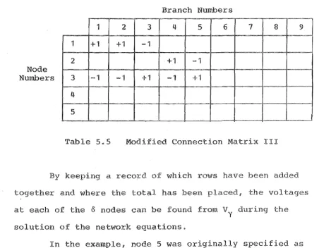
Modified Connection Matrix I Modified Connection Matrix II Modified Connection Matrix III
7 and 9 ON
KYI - 7
ONSquare Wave Coordinates
Star/Star/Star rms Voltages and Currents Star/Delta/Star rms Voltages and Currents Star/Delta/Delta rIDS Terminal Voltages
Quadrature Voltages and Thyristor Switches Necessary to Operate the Combined
Quadrature Booster/Bucker Fault Clearing Times
8.25 kVA Transformer Impedance Parameters Transformer Impedance Parameters
[image:16.595.90.531.128.814.2]abbreviations
given belowe
A
a.c.
Aal
b
n
B
aa
c
C
Ccc
C
n
cos
cos
C
aa,
D
d co
d/dt
e
1
, the
this
have the meanings
ampere
alternating current
ampere
centimetre
audio frequency
auxiliary inductance matrix
Fourier
auxil
alpha node
icient
inductance
discrete Four
coefficient
auxiliary alpha node matr
number of capacitive
capacitance
branch capacitance matrix
rms value of each Four
cosine
cosine
auxiliary
nodes
matr
prior
of
a thyristor
rate
change with re
in a network
component
to time
source of
ectromotive force
f( G
g( } G.E.C.R. G a.r h HC HR HV h.v.d.c. Hz I IAK I.E.E. I.E.E.E. j km
logical tion of
pules to a : functional notation
General Electric Company Division
Recti
auxiliary alpha node ~ res tance matrix integration step-length
maximum integration step-length during commutation
maximum integration length variable integration step-length high voltage direct current
hertz current
logical representation of thyristor anode-cathode current
: vector of capacitor currents
Institution of Electri Engineers
vector vector vector j2
=
-1ki
s
of and
res
currents currents thyristor currents
(103 hertz)
kV kVA kWs/kVA 1 L m M rnA mm ms MVA MVAr MW ,n ns p p
.
.
i i of and inductive(10;) volt)
lovo (103
kilowatt-second per kilovolt-ampere
number induc branches in a network inductance
branch inductance matrix
auxiliary inductance matrix of gamma nodes over-relaxation factor
logical representation of pulse output from monostable
milliampere (10-3 ampere)
mutual inductance between branches i and j auxiliary inductance matrix
millimetre (10-3 metre)
auxiliary res matrix millisecond (10-3 second)
megavolt-ampere (106 vo ampere)
megavolt-ampere reactive (106 volt-ampere
a
istance matrix
of ent state a thyristor
p.u.
Q Q r Rrms
ss
sin
t T -1tan
Th TIL TR ·TTLu
v
VA
unit
vector
number of
stive
a network
resistance
inductive branch resistance matrix
auxiliary inductive branch resistance
matrix
root mean square
revolutions
minute
:
branch resistance matrix
auxiliary resistance matrix of
nodes
second
back-to-back thyristor switch
sine
time
transformer
inverse tangent
thyristor
ion line
transistor
istor
volt or voltage
of
tor
VAr
V/cm
w
X X
y Z
cc
:
volt
vo
vector
vo
vector of node vo
vector
\l'latt
reactance
vol
a thyr
tor
across inductive
s across resistive
xx
matrix of capacitive branch susceptances
matrix of inductive branch reactances
number of thyristor branches in a network
impedance
nodes connected to at
capacitive branch
tone
nodes connected to at least one resistive
branch, but with no capacitive branch
connections
nodes connected only to inductive b
constant terms in implicit integration
state vectors
to at
one
f
of a thyristor
:
rotor
rotating
to synchronous
p
T
o %
< «)
1
F
microsecond (1
3 1416
6 )
by quadrature booster/bucker algebraic sum
monostable output pulse ,length
phase angle difference between voltage and current (i.e. power cos<j»
phase relationship of each. Fourier component
state vector coefficient matrix inductor flux
vector inductor fluxes angular frequency
ohm
square root degree
cent
approximately to s than (or equal to)
y y
symbols
1
..
source
ammeter
resistor
capacitor
inductor
earth
diode
thyristor
Zener diode
npn transistor
series transformer with windings
wound in opposition to each other
current trans
star transi- ...
m'oV'connection
three-winding transformer
three-phase four-winding transformer
voltage comparator
non=inverting buffer
inverter
two input NAND gate
ABSTRACT
on the the ating
1
ef both magnitude and phase shi control is proposed. Two back-to-back thyristor switches per phase are required, and device provides fast
continuously variable voltage magnitude and phase control at the expense of some waveform distortion.
A dynamic simulation computer programme, which is on state-space approach, is developed.
A three-phase control unit, to control the thyristor
switchings on each phase, is described and the theoretical waveforms are veri by both experimental tests and
digital computer Consideration is so given to the harmonic content produced.
Applications of the proposed thyristor-controlled regulating transformer to the problems of voltage
regulation, power trans control and improvement in the
ent stabi of systems are also
I am to my supervisor,
J.
Arril enthus andguidance throughout this project.
I wish to thank New Zealand Electricity their financial as granting of study
to enable this project to be completed. The Christchurch Draughting Section of New Zealand icity are so thanked
of the many il
their diligence in the preparation in s thesis.
The cooperation Mr J. 1, D the
Recti Division, General Electric Company, Great Britain, in the provision various of hardware is ly acknowledged.
During s project many hours have been in building hardware and computing. I wish therefore to thank the technical staff of the Department of Electri Engineering and the Computer Centre of the ity Canterbury for invaluable help expertise
Last, but most certainly not Q I wish to
express my to stine. Her as a
mother to Leanne
a wi
Timothy been
·her
1
CHAPTER 1
INTRODUCTION
In the advancement of power electronics component technology development of the thyristor must rank as one of the more important technolog achievements.
improved quality the silicon has enabled the diameter of the thyristor element to be increased, ting in
higher current ratings. Coupled with an improved reverse blocking capab ity, this made i t possib to increase the power handling thyristors These
advancements in thyristor technology have made the possibility of high-power thyristors a reality, and
individual thyristors with power ratings in the MVA range are commercially availab
During the 1960's thyristors had been developed to such an extent that they could replace mercury-arc valves in some industrial applications, their application to h.v.d c. transmission systems was considered when extens to the Gotland h.v.d.c. link were mooted Thyristors were
in the extension in 1970 and their
iority over arc valves (Martens son 1975)
Since 1970 thyr s have led in most h.v d.c. (Martens son 1975) and the ined in the
se s
,
in toin a network and (1971), Sundberg (1976) Schwei
(1978) are but of terns 0
The simplest form of a thyristo I voltage ator employs a r back-to-back thyristors
connected in with a load (Fig 1.1) By varying
phase-angle delayed gate pulses to the thyristors and firing them symmetrically with to zero crossings the supply voltage (V
s )
the load voltage (VL) can varied, depending on the load power , from zero to full load voltage VS. Although a wide range vol control is possible, the thyristors must be to both full load voltage and current, and the harmonic stortion of
load voltage is most severe.
t
" 1 1
s
istor~Control VoThe of harmonic stortion is
overcome ign a thyristor
(Marshall 1974) wh uses thyristor switches
to tappings. The trans th
in ser with or bypas
by to the
output vol a
non-voltage is by
The provision of a I trans th a large number of secondary windings for voltage control together with four thyristors secondary winding, each
to I load current, would prove to be uneconomic for many applications.
A recent publication (Arrillaga 1976) a single-phase thyristor-controlled regulating transformer for voltage boosting. on the principle of the regulating transformer booster (Westinghouse 1964), this device boosts the load voltage by means two phase-controlled back-to-back thyristor , providing fast and continuously variable voltage boost at the expense of some waveform distortion. With this device the regulating transformer is only handling a small proportion of the transmitted power, and the four thyristors need not rated full load vol and current
The work described in this study involves
singl led
trans , as by (1976) ,
s both
the use of a phase displaced
a
regulation, voltage to
From
a
This was to
e
are
control the
the
of
back thyristor switches so a assessment of the ity of proposed system could made
Complementing 1 assessment the
3
proposed circuit, a computer programme based on state~space
techniques has so been written. The mathematical model used the development of the computer programme is presented in Chapter 4. Chapters 5 and 6 deal with the actual programme, discussing operation and per
An evaluation, both by laboratory measurement
computer simulation, of the use the proposed as a means voltage regulation is ented in Chapter 7. Using a quadrature regulating tage, the ability the proposed circuit to provide power transfer control in transmission circuits investigated and discussed in Chapter 8. The fast-acting nature the proposed c is exploited in 9, where the injection
voltage is to control the transient stability of power
Finally a ion ts
during
CHAPTER 2
Presented in this chapter a full description the operation the proposed circuit, both as an in-phase and quadrature voltage and an and
quadrature voltage bucker. Theoretical waveforms are also presented along with the firing requirements for each thyristor.
2 • 1 PROPOSED
The schematic diagram of Fig.
2.1
shows one phase of a thyristor-controlled in-phase volinterconnecting two systems represented by their respective voltages V
Q and VR• Shunt transformer T1 provides the in-phase voltage (V
S) each phase and series transformer T2 the controlled boosting voltage.
S1 and S2 are two back-to-back thyristor swi
The second thyristor switch (S2) to the
winding 51 is
I in to
current, causing
1 sing
and endangering the insulation winding.
Reversing the sense the secondary winding the
ser trans converts vol
of Fig. 2 1 into an
Th1 Th4
Fig. 2.1 Bas In-Phase Voltage Booster
2. 1 • 1
The operation of the in-phase voltage booster
(Fig. 2.1) can be with r to the
theoretical waveforms of Fig. 2.2. These waveforms correspond to a lagging power factor (~) and if the thyristor switch S1 is triggered without delay (i e. at the zero crossings of the current waveform) a constant sinusoidal voltage added to the voltage VQ and
with it.
The s €1 £2 (meas
zero
in S1 and S2
tor of S1 can at any the range ~ < £1 < 180°.
Simi ly, the appropr thyristor 8
I
1
Th2
Th3 Th4
• 2 2
¢.J
•I
i7T----'
wt
wt
wt
wt
wt
both manner.
At
current (I) , when V
Q
forward-bias and provision a
8
1 82 the
1 is istors 3 and 4 are
ed
pulse to thyristor 3
ly. 11
turn ON, thus short-circuiting the secondary winding of
T20 VT , the voltage across the secondary winding of T2 , is now equal
thyristor 3.
where
V
f is the forward voltage drop
With thyristor 3 conducting V8 positive,
thyristor 1 is forward-biased and a pulse to thyristor 1 will turn i t ON. V
T now ,
reverse-biasing and turning OFF thyr 3. When Vs is ive, thyristor 3 is again Hence the
thyristor 3 will turn i t ON and a commutation from thyristor 1 to thyristor 3 will take place, turning thyristor 1 OFF.
Operation during the second hal Ie current is
polarities
to the t, but with and with the
1 voltage st.or
one complete are
.
2.2102
As t
.
2. 1can when sens
of T2 is revers The
t
voltage
wave • 2. 3 •
The
be triggered at any
a lagging power to
within the
switch 8
1 can
°
e 0 < £1 < <P,
and the appropriate thyristor of switch 8
2 can be
triggered at any time within the range <p < £2 < 180°. Therefore the ing of switches 8
1 and S2 can control
the voltage bucking
At the beginning of the positive half-cycle of line current with thyristor 2 conducting, the voltage V
T is Vs + Vf which forward-biases thyristor 4. Firing thyristor 4 reduces V
T to +Vfl reverse~biasing thyristor 2
and forcing i t to turn OFF. When Vs changes polarity thyristor 2 is again forward-biased. The provision of a
gate pulse to thyristor 2 will therefore turn i t ON and a commutation from thyristor 4 to thyristor 2 will take place, turning thyristor 4 OFF.
During the second half-cycle of line current the operation of the voltage bucker is similar to the first, but with all voltage polarities reversed and
the thyristor pair
Th1 Th2
Ttl 3 Th4
1
2 2
F one e
a booster
interconnecting two by voltages
V
Q and VR respectively. The vo each is provided by shunt transformer T1, the
T2 provides the controlled quadrature boosting voltage. S1 and S2 are two back~to-back thyristor switches, and the quadrature voltage represented by
• 2.4 Bas
The same as described in voltage can
I
•
Th4
Th2 Th3
Vol Booster
quadrature voltage booster is voltage booster, which has been
2.1.1. The quadrature or lag the
and depending on the phase f
em voltage V Q
components of V
Q I I a of
di modes of are e.
modes (i) and (ii) a
voltage and ~, lying in the
o
°
~ ~ < 90°
Iis lagging and leading s 5 and 2.6 show the respective waveforms modes (i) and )
.
Using a lagging quadrature voltage, when ~ in the range
90
°
< ~ ~ < 180°, th . e ClrCUl " "t 0 f F' 19. 2 4 . opera es 1n t "(iii) and (iv) ~ lagging and leading respectively. Figs 2.7 and 2.8 show the respective theoretical wave for modes (iii) and (iv).
The quadrature voltage booster shown in Fig. 2.4 is converted into a quadrature voltage bucker by reversing the sense of the secondary winding of the ser trans
Quadrature voltage bucker operation is the same as e in-phase voltage bucker which was discussed in Section 2.1.2.
As with the quadrature voltage booster, the
quadrature voltage bucker can also operate in a number of different modes. Modes (v) and (vi) have a leading
quadrature voltage and ~, which lies the range
lagging and leading tively. F 2.9
and 2 10 show theoretical waveforms modes
(v) (vi). When ~ 1 the
voltage and the operational ~ lagging and ng are
(vii) and (viii). The
for modes (vii) i) are shown Figs 2 11 and 2 12
1
I wt
wt
'15
wt
wt
wt
I wt
wt
I
wt
wt
wt
I wt
wt
V T
I
V R
I
I
I
I
I
I
i
s11
Fig~ 2.11
1
wt
wt
wt
wt
wt
s1
S1I
wt
wt
wt
I wt
[image:46.595.125.467.77.759.2]21
Bes of discussed in
s is sible to the quadra-ture
vol booster or rcuit a number modes. For
,
if for mode (i) a laggingvoltage used than a leading voltage
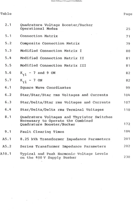
the theoretical waveforms of Fig. 2.13 are obtained. appropriate thyristor of switch 8
2, required to terminate the voltage boosting period, reverse-biased until the zero crossing of the line current (I) cannot conduct until that instant. But even then the conducting thyristor
switch 81, being still forward-biased, will continue conducting and the switching of 8
2 will immediately short-circuit the secondary winding transformer T1 " To
overcome this problem a delay (A) could be built into the control system to allow 8
1 to switch OFF and recover fully before ing of 8
2. This delay, however, would cause a temporary open-circuit, with large overvoltages, across the secondary winding of T2 and is not considered a
practical proposition.
In some cases, the resultant waveform VR is ident 1
with that obtained from one of the eight modes already
discussed. For example, if a lagging rather than a leading quadrature vol is
resultant
mode (v)
identical with that
ion the
mode (i). F . 2.14 shows mode (v) operation with a lagging voltage, and a comparison of
shows the resultant similarity in VR.
'--., wt
I ~"H----~--~----+-. wt
[image:48.595.119.458.72.767.2]2
I
Us modes of
in s and summarised in
2.1 i t sible to phase r
or The fi ng
angle Ie for control the
thyristor switches S1 and are also listed in Table 2.1. It can be seen from th Table that if ~ is leading or
1 ng by 90° the firing ranges of 8
1 and 82 are either reduced to 0° or over 180°.
If ~ should be ther leading or lagging by 90°, then neither the quadrature booster nor the quadrature
bucker will operate as described in Sections 2.1.1 and 2 1.2 ively. This is because the line current is now
either in-phase or 1800 out of phase with the quadrature voltage and the thyristors of switches 81 and 82, which are not forward-biased at the appropriate times, cannot switch in their correct sequence. There are two alternative
solutions to this problem: ther switch 81 or switch S2 can triggered without delay at the zero crossings of the current waveform. If switch 81 is triggered without delay, then depending on a boosting or bucking circuit i being used, a constant sinusoidal voltage will be
to or tem voltage VQI i
maximum phase the fundamental of When triggered thout del the voltage V
Table 2.J. Quadrature Voltage Booster/Bucker Operational Modes
Phase Angle Difference Range of Firing
I
ofbetween V S and I Angle for Switch for Switch Mode Circuit Voltage
(<P) 81
(i) booster leading lag 90° + <p < E < 1800 00 < E < + <p
00 < $ < 900 1 - - 2
-booster leading lead 900 -$ < E < 1800 < C' < 900 _ $
00
..2.
$ < 900 1 - - ~2( i i i )
I
booster lag 90° - (180° - $) < E < 1800I
0° < < 900°
900 <$'::' 1800 1 - - 1::2 (180
-( booster lead
+
(180° - ¢) < E1 ,2.1800 00 < < 900 + (180° .:.. cb)900 < ¢ ..:: 180° _ E2
(v) bucker leading
0° <
lag
$ <900 0
0 <
- 1::1 < 90° + $ 90
0
+ $ < 1::2 ..::
-lead I
bucker I 0° < < 90° -¢ 900 - $ < E < 1800
00 ,2. $ < 900 _ El 2
-(vii) bucker
90° < ¢ ..:: 0
0
< <
_ El 90° - (1800 - ¢) 900 - (1800 - ¢)< E < 18
2-(viii) bucker lead .::. El < 900 + (1800 - <1» + (1800 - < E2
..2.
180°
90° < $ ,2. 180° I
2 3 THYRISTOR
For successful the ter or
c (both and ) v
study must when a pulse must be
provided for thyristor and also the at which a.
gate pulse must not provided. These times, the provision or non-provision of pulses, can be
ascertained from theoretical waveforms discussed in previous sections of this chapter.
In Section 2.3.1 any to a "booster c
to both in-phase and quadrature boosting. Likewisev
in Section 2.3.2 any reference to a "bucker circuit" re to both in-phase and quadrature bucking.
2.3. 1
The gate pulses con)crolling the ing of the thyristors of switch S1 are phase~controlled with
to voltage VS. Logic, derived from the circuit voltage and current waveforms, is used to provide the gate pulses for the thyristors of switch S2 and a careful examination the
theoretical waveforms (Figs 2.2, 2.5, 2.6, 2 7 and 2 8) is necessary to
conduct over positive 1 vol
the correct log Thyristor 3 must sting va
current (I) the applicat thyristor 1. Condit are again thyristor 3 to conduct during the
(V ) S of the
of negative voltage
Vs
line current, and theof 3 occur at any time after Va goes
'"
but of thyristor' 3"
2.3 2
For the pulses
firing of the thyristors 8
2 are
controlled with to vol V The
8 pulses
thyristors switch 8
1 are provided by logic
derived from the circuit voltage and current waveforms. ing to the theoretical waveforms of Figs 2.3~ 2.9
2
10,2.11
and2.12,
thyristor 2 must conduct over the period of positive voltageVs
and itive 1 current Ithe ing of thyristor 4. Thyristor 2 may again be provided with gate pulses at
negative and before I goes negative.
time
Vs
goes conduction requirements for thyristor 1 are similar to, but di1800 , those of thyristor 2.
2.4 USE OF A TRANSFORMER
If the connection between two systems (V
Q and VR)
made via a power transformer, the shunt transformer T'I Fig. 2 1 can be dispensed with required reduced voltage obtained from a iary winding. F . 2.15
a s diagram of a where the e
to neutral tert vo are wi,th the
vol
V
Q and Thyristor control produces the wave~ 27
• 2.2, upon revers the sense of secondary winding of T2 the wave illus in . 2.3 can (i e. the circuit can act as
an vo or bucker). In 1
8 1
Fig. 2.15 In-Phase Voltage Booster
accomplished by making use of the interrelationships between the voltages on star and delta connected wind of a three-phase transformer. One possible set of
transformer connections illustrated in the quadrature voltage booster of Fig. 2.16, where the line~to~l
tertiary voltages will be in quadrature with the line to neutral voltages of the star connected primary and s windings.
I
3
THE CONTROL UNIT
A three-phase control unit, thyri
vol regulator, was built to produce direct the firing pules to the appropriate thyristors. The product of ing pulses, together with the assoc
circuitry, is discussed in this chapter. This control was built so that a laboratory assessment of the
of the operation made.
the proposed system (Chapter 2)
3.1
GATE PULSE DERIVATTo ensure the successful firing of a thyristor the gate should be provided with a high frequency train of pulses with rising edges. If the first pulse of the train does not initiate conduction then more pulses are applied to the thyristor until conduction is in
The gate pulses for the phase~angle 1
thyristors, swi S1 (Section 2 • .1 )
and S2 for 2 p .2) f are
commercial pulse circuit. Any thyristor wh is not cant led, switch S2 for
operation (Section 2.3.1) and
(Section 2.3.2), must conduct whenever
controll not conduct. The firing pulses -thea are ived from the ci current and vol
are as log control
3. 1 Q 1
The e control of a b of thyristors two high
one each thyristor. These two must be the re
A pulse train ring circuit (RIS54) produced by the General ic Company ,,- Recti Division (G E.C R.)
(Appendix 1) is used to provide pules This circuit provides two outputs, separated by 180°, of
100 ~s pulses with a r time of 500 ns. A of controllability between 15° and 165° is achieved with a control signal of ±5 V d.c., and calibration of firing circuit is ibed in Appendix 2. To ec ly
the firing circuit from thyristors, each ing circuit output is connected to the appropriate thyristor of the phase-angle controlled pair via a pulse transformer
(Appendix 3) as shown in Fig. 3.1.
Firing Circui-t Output
1N4148
1N4148
39R
Thyristor
, - - - - Q Gate
Thyristor
---0
Cathode PulseTransformer
Fig 3 1 Interconnection Between Fir Thyristor
3 L
Re ing to
current waveforms VS' VT
waveforms are
2.1 and 2.4,
I are contro the c
and in the
istors. All by transformers, the current waveform being across a non~
resistor. The waveforms are then fed into type "710" voltage comparators which give a TTL compatible output.
3.1.2.1 It
possible to have one set of logic which will control thyristor switch S2 both in-phase and quadrature
31
boosting. Referring to Figs 2.2, 2.5, 2.6, 2.7 and 2.8, i t can be seen that are two distinc·t conduction periods per cycle each thyristor of switch S2" During each these four separate conduction periods there are di nct relationships between the waveforms Vsr VT and I. In Fig. 3.2 the waveforms VS' VT and I are reproduced from Fig. 2.5. These waveforms are used by way of example and any of the other four sets could have been used.
From the logical representations of the waveforms Vs and VT in Fig. 3.2, it can be seen that one of the conduction periods for each
defined by the respectively. To thyristor 3, the log waveform I is to
of length T. The logical
identify conduction
thyristors 3 and 4 can be
·V
'r
andconduction
ion of the current fol:'
a monostable, producing pulse sion
M30r
used to iod of thyristor 3 u the second conduction period of stor 4I
I
I
M4 I Vs +
M3
I Vs
V T + M401stors 3 4
are by logical (3. 1)
and (3 2) ly
VS0VT + M3"r (3. 1 )
·V T + Mq, I (3.2)
The circuits used to produce the log expres
( 3 . 1) and ( 3 . 2 ) thyristors switch S2 are shown in Fig. 3.3. The outputs of TTL logic circuit give a logic level
'1'
when the particular thyristor i t serves must conduct, and a logic level '0' at all other times.3.1.2.2 One logic
circuit is used to control thyristor switch S1 for both in-phase and quadrature voltage bucking. Each thyristor of switch 8
1 two conduction periods per cycle (see 3
Figs 2.3, 2.9, 2.10, 2.11 and 2.12). To i1 how the logic controlling switch 8
1 is derivedu the waveforms 'VT
and
r
from Fig. 2.9 are reproduced in Fig. 3.4. From the logical representations of waveforms Vs and r in Fig. 3 4, i t can be seen that one of the conduction periods for each of the thyristors 1 and 2 can be defined by the log 1sions VS·I and vS"r respectively. Each of these
conduction shown ing into the region where thyristors 3 and 4 are ing. Thyristors 1 2 are
at time a commutation from tch 81
to tch S2 will take place turning thyristors 1 2 OFF. To de the second iod conduction
thyr tor
1,
the logical representation of the currentwave-.
V T
. 3.3 Booster Logic
I
I
t11
I---"=--!:---+----"--M
10r
M· I 2
Vs I + M1"I
Fig 3.4 Operation Logic
The used to
conduction 1. In a simi manner, the
conduction thyristor 2 by
s I conduction
thyristors 1 and 2 are y fined by 1 ions (3.3) and (3 4) respectively.
or
+ M, I (3.3)VS'I
+
M20I (3.4)The circuits to the logic expressions (3.3) and (3.4) for the thyristors of switch S1 are shown in Fig. 3.5,
3.1.2.3 The
TTL logic output from the circuits illustrated in 3.3 and 3.5 does not offer sufficient power to a thyristor, and a high frequency pulse train is more desirable than a
ring pulse. For these reasons a known as a "Microne" pulse transformer (Appendix 4) is used as an output stage from the TTL logic circuits.
Using the circuit shown in Fig. 3.6, the TTL logic output is converted into a 12 kHz pulse train. The
trans TR1 and amplifies the TTL logic pu e and the "Microne" pulse transformer, which s on a di
only the
input
Although the "Microne" trans i t not af the thyristor the
se trans
, outputs a 12 kHz pulse 1 TTL
is
pulse, as a pulse
electrical isolation between There
(Appendix 3)
v
S o---l1I
I
* 3 * 5
V "I S
v .
IS
M" I
L.
Bucker Operation
-
-V · I + M · I
S 1
c s
To tor
1
To istor
Non-Inverting Buffer
390R
TR1 PN3643
F ,,3.., 6
1K
2K2
15R
100
1---1-00
+
INPUT
0.001
ov
C
OUTPUT
C1
1
+
0 - - + - - - 1ov
"HICRONE"
Trans-former 1N4148
"Microne Pulse Transformer
Cathode
3.2 ~T~HE~~~~~~~~~~~V~O~L~T~A~G~E~~~~~
A unit, istor~controlled
regulator shown in 3.7(a) and (b), has been built to control switching two
of thyristors per phase. The unit is to in conjunction with an 8.25 J<:VA th
transformer (Appendix A5.1) and
three~·winding
series transformers (Appendix A5.2), where the tertiary voltage used
to control the secondary voltage of the 8.25 kVA transformer. Typical per phase connections for the
three-phase transformer, series transformers and control unit are shown in Figs 2.15 and 2.16.
The three-phase control unit shown in Fig. 3.7(a)
consists of three identical single-phase control units. The operation of anyone of these units is completely independent of the other two, and the following
description the unit only to each single-phase unit.
The thyristors in each back-to-back pair, 81 and
82, are rated at 25 A rms and are type 10RC60A manufactured by International Recti Both thyristors of each
back-to-back are mounted onp but cally i
, a s of heatsink and s
with the two pulse transformers, mounted on ilVeroll
In all e components, with the exception of the G.E.C.R. firing
voltage transr~rmg
•
•
..
•Fig. 3.7 (a)
•
.
,-• -•
..
•
•
•
-_.
,-•
..
•
• •
The Thyristor-Controlled Voltage Regulator - Front Vi ew
.,
•
•
..
+=
terminals for
of Figs 2.15 and 2 16
a 38 V or 66 V
norma used as e-angle
switch (Section 3.1.1) 38 V or 66 V input vo transformed into a 200 V rms centre tapped
directly to theG.E.C.R. firing The pairs terminals lab
tor
are the input terminals for the corresponding waveforms, which are isolated from the main by transformers and used to determine the logic for firing the log control
thyristors (Section 3.1.2). These three inputs, together with the +14 V, +5 V and -5 V power supplies for the
integrated circuitry are routed to the mode swi which is a four position eight pole switch. In each control unit, provision has been made up to four logic to be
ng of the accommodated. These logic boards control the
appropriate logic controlled thyristor tch, and each of the four mode switch positions corresponds to one of these logic boards. As each position of the mode tch
, the input waveforms Vs V
T and and the log power suppl s are routed to the appropriate logic
For .us
ent mode 1
the mode (see Figs 4
(Fig. 3.6) . The
only two mode
voltage booster I and
are
ion. The remaining two poles on route the two outputs logic board
3.5 for the log of 1 and to two IIMicroneli
(Figs 3.3 and 305) by a the resistance
component the e timing c
Timing components to a
T from 1.5 to 15 ms.
The a two e
switch which switches the and
controlled firing pulses between thyr switches 8 1
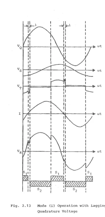
S2" Fig. 3 8 is a diagram showing
to boost/buck switch, connection shown is
duplicated again to cater both the positive and negat fi!ing pulse connections to the pulse transformer .
To Th 40---_8
To Th
To Th
20---.
To Th 1
0---_.
... ---0
To Th '1_---oFrom "Microne"
Output 1
... - - - o T o Th 2 From "Microne"
'1>=---0 Ou t put 2
_ - - - o T o Th 3 From G"E"C"R"
"""'---0
Output 2e---QTo Tb 4
From G.E.C.R.
-,---0
Output 1I BOOST: BUCK
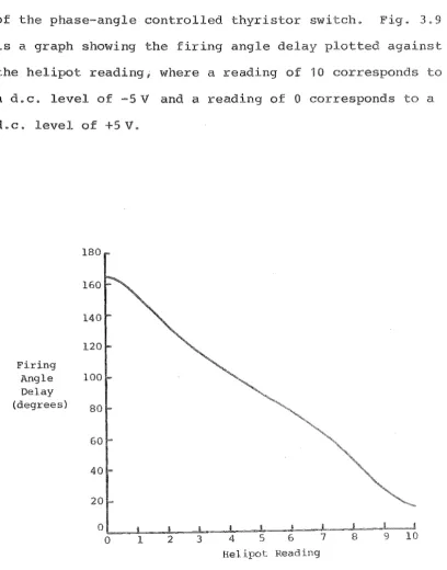
[image:69.595.92.518.378.767.2]phase~angle firing pulses 1 and 2) is adj via the multiturn helipot, and an ind
the f ing angle (in is given on the meter mounted on the control unit. Use multi turn ,hel allows fine adjustments to be made to the ang
of the phase-angle controlled thyristor switch. Fig. 309 is a graph showing the firing angle delay plotted t
helipot readingi where a reading of 10 corresponds to ad. c. level of -5 V and a reading of 0 corresponds to a d. c. level of +5 V.
Firing Angle Delay (degrees)
. 3 9
180
160
Firing Angle
Helipot Reading
t
[image:70.595.93.502.245.766.2]ly, cons was
the operation vol c
the booster. The turn OFF of the thyristor tch 8 1 triggered the conduction
icularly ng the alternate thyristor ng in the tert
of the three-phase transformer being the conducting thyristor of switch 8
1 turns OFF the
alternate thyristor forward-bia and any rapid change of this forward anode to cathode voltage can produce a transient gate current (Ramshaw 1973) resulting in the alternate thyristor turning ON. To overcome this problem and lower the rapid changes in voltage across the thyr tors, both snubbers and
circuit.
reactors were introduced into the
Each snubber consists of a series resistive~
capacitive network connected across each
thyristor pair. This technique for lowering the rapid changes in voltage across the thyristors relies on the integrating ability of the capacitor.
The low tertiary winding leakage reactance, as measured by standard short-circuit tests, of the
transformer results in very short commutation times
consequent rapid in vol across thyristor The addition a reactor, bet,ween the
thyristor the commutation times and
thereby the rapid voltage changes.
In the following discussion of protection, any devices re
Internal
to are those shown Figs 2.1 and 2.4. which cause the maloperation of the
switching sequences must cleared by open~
circuiting the winding T1 and
circuiting the winding of -the es trans T 2 " Shorting the secondary winding of T2 avoids
magnetising current, which cause s and endanger insulation.
Any internal faults causing the simultaneous
conduction of both thyristor switches and consequent short~
circuiting of the transformer winding T1 require the provision of fast-acting Water were used thyr tor protection in the thyristor-controlled voltage regulator and they were placed between switch S1 and transformer T1 on each phase.
Fai of a thyr normally results in a short-circuit across the device. If such a lure occurred in either of the thyristors of switch S1' then the fast~acting
fuse would IIblow" as soon as the appropriate istor
switch S2' causing the winding of T1 to be short-circuited, was fired. Assuming the proposed circuit was operating in
a booster mode, the logic (Section 3.1.2.1) would ensure that only the thyristors of switch S2 were fired, leaving the transformer winding T1 open-circuited. Should a failure of one of thyristors of switch S1 occur ng
as a voltage , u p o n fault (Le" the "blowing'! the fuse) . the S2 must be triggered at the current waveform (I) zero crossings,
ircuiting the secondary winding of the ser s
transformer T2 Provision of this type of protection not inherent the i t log 3 • 1 • 2 • 2 ) and
1 protection logic is neces a I sca
of project).
A
ts a II
bucking operation, e sa
the thyristors bot,h as soon as ,the
switch
"blows" the winding T1 is open~circuited and the secondary winding of T2 short-circui by the
iled thyristor. Provision was not considered
protection against external faults for the thyristor-controlled voltage regulator described in this chapter. However a full scale device would require th type of protection.
L! 7
Upon the detection an external fault the thyristor switch 8 1 can immediately be blocked, leaving the switch 8 2 to
CHAPTER 4
THE
The mathematical model developed in is ifically formulated to cater for res tance, inductance and thyristor circuit elements only. Built up from these three circuit ements, a mathematical model is defined for each of the relevant system components.
Limitations are imposed on the way in which these tem components may be interconnected This is done to increase computing efficiency and does not severely re the representation of system configurations.
In the analysis diakoptical tearing techniques are applied to the various elements and sub~networks. This enables that portion of the network affected by topology changes, due to thyristor switchings, to be isolated the remainder of the system.
A state-space approach used in the analysis of the system equations, thus allowing a unified treatment
elements. The both and non-l
state integration.
To
are solved by numer
tem components such as filters to be modelled, a more complex mathematical model which includes
as well as res , inductive and thyristor c ements, is developed in Appendix 6. This
4 , to discus in 5, has
to include these ements. The
programme has been written in this way so l:hat can
in the analysis conf other than
those discussed in this study.
4 • 1 COMPONENT
The system components are:
1. The a.c. system~ the individual components of the a.c. system may not be of particular importance, but
overall combined effects are.
2. Thyristors; the bistable action of each individual thyristor must be represented to enable an accurate simulation thyristor switching.
3. Transformers; the transformer model must accurately represent fects such as phase shifts and neutral earthing which are inherent in the various three~phase
transformer connections.
4. Transmission lines; transmission lines are normally operated under balanced conditions and a "
"
representation is therefore quite adequate.
4. 1 • 1
Normally an a.e power tern to
low-order harmonic is of an inductive nature. The simple equivalent circuit of Fig 4.1, where the source impedance Z
=
R + jWLs ' can there be used to s s
e
Fig 4.1 Simple A.C. System
However is 0 to ent a
over a range frequencies. g. 4.2 illustrates an alternative equivalent circuit which has been proposed by Bowles (1970) and maintains an almost constant impedance angle for low~order harmonics. For the equiva
of Fig. 4.2, Rs and are chosen to give the source impedance Zs' and Ra is determined by the impedance angle at fundamental frequency.
Fig 4.2
4. 1 2
R a
lU
stors The thyristor
e
A C,
L /2 s
entation
s a basic bistable state cannot be deduced in every case sent values of voltage and current at
and
some is known
A simple digital model of a istor must lude table
(1973) have ed a
model which th and employs a
minimum of input functions, whose values are usual
required other purposes within the digital simulation 0
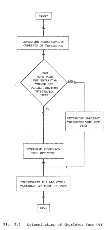
The state of each thyr is determined at the beginning of every integration s , and the current through the thyristor is then calculated assuming this part
state throughout the complete integration step. The value this current then used to indicate the state
thyristor for the next integration The thyristor model
information:
the following
anode to cathode voltage (V
AK) , at logic for a forward-biased device and logic 1 a reverse-biased device.
1 "1 v
'0' for
anode to cathode current (I
AK), at logic level '1' when the current is than holding current and logic level '0 1 when i t is less than
holding current.
the thyristor ing state (D) immed
to the ; at logic '1 i
the ON at logic level '0' when the OFF.
of (G) is indicated by
The ent state (P) of the thyristor thus
given by the lowing sion
P
4.1.3
The traditional transformer equivalent c t (Say 1958) is not suitable a 1 dynamic analysis, because dif transformer connections 0
different impedances to components of current and the phase shifts inherent in the different connections need to be represented.
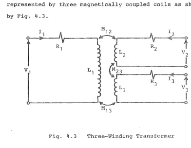
A single~phase three-winding can
represented by three magnetically coupled coils as shown by Fig.
4.3.
I1 M12 12
I
R1 R2t
L2 V2
I
V
1 L1
R3 I3
L3 V3
I
Fig. 4 3 Three~Winding Transformer
[image:78.595.68.461.402.706.2]Since trans
Z11 Z12 Z13 Z21 2 Z23 Z31 Z32 Z33
s are not
(l~ 1)
relative motion with respect to each other or to any other magnetically coupled ci I the impedance matr
must be symmetrical about the diagonal (Le. Z12 ::;; Z21 p
Z13 ::;; Z31 and Z23 ::;; Z32). The matrix equation (4.1) can therefore be rewritten in the following form:
d +
o
o
(4.2)The single-phase transformer model depicted by
matrix equation (4.2) produces a magnetising current which based on the assumption linear core magnet ation. It is possible to cater for non-linearities in the core magnetisation (i.e. saturation) provided the relationship between the equivalent circuit and the magnetising
characteristic established. However, the introduction of former non~
a 1 throughout.
beyond core
scope of this is assumed
In , three-phase three-winding transformers can by 1 9 x 9 impedance matrices.
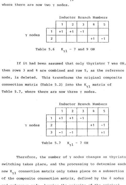
There is however
a
concerningnot to
cal di iculty in obtaining data e mutuals, because manufacturers have
imposs to model 9 x 9 impedance matrix.
the
This was
of inductance
as a full formulation
(see equation (4.15)), and the tight coupled windings
an ill-conditioned (Conte 1965) inductance matrix which was impracticable to invert Consequently all three-phase
transformers are as being three independent single-phase trans (i.e. there are no interphase coupling terms the impedance matrix). This is an accurate representation for transformer banks of single-phase units and reduces the equations to three independent sets, one representing each phase.
To implement this coupled circuit model of the
transformer, accurate determination of the self and mutual impedances
impedances
required (the determination of e discussed in detail in Section 6.3.1).
When these impedances have been obtained, any effects such as phase shi and neutral earthing are automati ly catered for by the terminal connections.
4. 1 .4 sion Lines
Transmission are normally operated with Although lines are not equilaterally, and may not be , the
ssymmetry is slight, and phases can be considered to be balanced. The importance of stributed
and current with the