© 2016 IJSRST | Volume 2 | Issue 3 | Print ISSN: 2395-6011 | Online ISSN: 2395-602X Themed Section: Science and Technology
Multiband Reconfigurable Microstrip Patch Antenna
Hemantkumar Mane, V. U. Deshmukh
VPCOE, Baramati, Maharashtra, India
ABSTRACT
Reconfigurable Antenna is an alternative to band Antenna. Different techniques are used to achieve multi-band and widemulti-band operation of antenna. Reconfigurable antenna has a potential to add some functionality to mobile communication. A reconfigurable antenna is another solution to achieve multiple bands by switching ON and OFF some part of the antenna. To allow the operating frequency and the bandwidth to be reconfigurable switching components are normally used. In this paper microstrip patch-slot antenna is capable of frequency switching at different frequency bands from Frequency range. RF p-i-n diode is used for the switching purposes. The main aim of this paper is to provide multiband functionality form a single band frequency just by optimizing the antenna structure.
Keywords : Microstrip Patch, Reconfigurable antenna, optimization, PIN Diode
I.
INTRODUCTION
Wireless communication systems are attracted toward multi-functionality. This multi-functionality provides users with options of connecting to different kinds of wireless services for different purposes at different times. It is very important to develop single radiating element which is having capabilities of performing different functions and multi-band operation in order to minimize the antenna's weight and area. An antenna that have the ability to modify its characteristics, such as operating frequency, polarization or radiation pattern is referred to as a reconfigurable antenna. Reconfigurable antenna is used for to reduce the number of antenna necessary for Multiband function, but they can also be designed to work in complex systems such as emerging applications include software defined radio, cognitive radio, MIMO systems. Re-configurability can be achieved using slot configuration in the microstrip rectangular patch antenna with switching devices are connected inside the slot with ON & OFF State working. Switching devices such as PIN diodes, MEMS switches and optical switches are used for switching purposes.
This paper provides detail information of all type of reconfigurable antennas. Section II introduces the concept of types of reconfigurable antennas. Section III
presents Design parameters of reconfigurable antenna. Section IV presents optimization of structure. Section V presents result and conclusion.
II.
METHODS AND MATERIAL
1. Reconfigurable Antenna:
Antenna reconfiguration is broadly classified as frequency, radiation, polarization, radiation and frequency reconfigurable antennas.
A. Frequency Reconfigurable Antenna
Latest communication systems demand transmitters and receivers with multi-band operation, as a result different techniques for achieving frequency reconfigurability have been proposed in system where weight and area are critical issue.
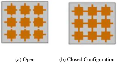
each small patch as shown in Fig. 1(a). As a result, the antenna resonates at a higher frequency band. On the other hand, when all switches are turned ON, the antenna effective area is clearly larger than the area of a singular patch array. The antenna accordingly resonates at a lower frequency band as shown in Fig. 1(b).Fig. (a) Antenna geometry when switches are turned OFF (b) Antenna geometry when switches are turned ON.
(a) Open (b) Closed Configuration
Figure 1: (a) Open and (b) Closed Configuration
B. Radiation Pattern Reconfigurable Antenna
Radiation pattern reconfigurability is based on the some modification of the spherical distribution of radiation pattern. Pattern reconfigurable antennas are usually designed using movable/rotatable structures or by using switchable and reactively-loaded parasitic elements. The antenna is designed to be able to reconfigure its radiation pattern during operation such that it maintains its broad pattern in the absence of interferences, and is capable of narrowing its pattern, when the interfering signals arrive at the antenna, to suppress these undesired signals as much as possible.
The total radiation pattern from the microstrip antenna originates from three things: direct space wave, edge diffracted space wave and edge diffracted surface wave. The Basic idea about the pattern reconfigurable antenna is antenna mounted on electrically thick substrates so that edge-diffracted surface wave field can be strong and which is having the magnitude higher than the diffracted space wave field.
C. Polarization Reconfigurable Antenna
Polarization reconfigurable antennas are capable of switching between different polarizations modes. The
capability of switching between horizontal, vertical and circular polarizations can be used to reduce polarization mismatch losses in portable devices. Polarization reconfigurability can be provided by changing the balance between the different modes of a multimode structure. Antenna with polarization diversity is very important due to the rapid growth of wireless communications and radar systems.
D. Radiation and Frequency Reconfigurable Antenna
In general, most antennas are capable of either frequency or pattern reconfigurability. However, they can be made a combination of both frequencies and pattern reconfigurable simultaneously. Frequency and Pattern reconfigurable microstrip antenna are done by using multiple switch connections.
2. Design Parameters
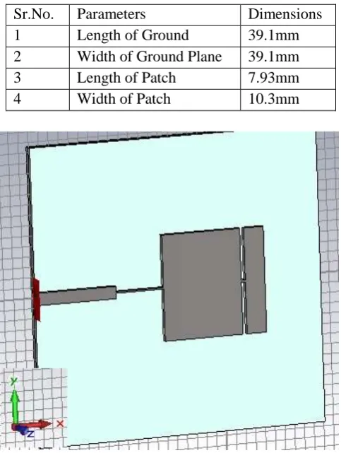
The basic structure of the proposed antenna, shown in Fig.2, consists of 3 layers. The lower layer, which constitutes the ground plane, covers the partial rectangular shaped substrate. The middle substrate, which is made of GML 100 has a relative dielectric constant єr =3.2 and height 1 mm. the upper layer, which is the patch, covers the rectangular top surface. Simulations were performed using CST Microwave Studio.
Step 1: Calculation of the Width (W):
The width of the Microstrip patch antenna is given as
2
1
2
0
r
f
c
W
Where, C is velocity
of light,
f
0
is Resonant Frequency & εr is Relative
Dielectric Constant of Substrate.
Step 2: Calculating the Length (L)
Effective dielectric constant (εre)
effective dielectric constant approaches the value of the dielectric constant of the substrate is given by:
Effective length (Leff)
Length Extension (ΔL)
Length Extension (ΔL), which is a function of the effective dielectric Constant and the width-to-height ratio (W/h).The length extension are:
Calculation of actual length of patch (L)
The length is a critical parameter and the above equations are used to obtain an accurate value for the patch length L.The actual length is obtained by:
Lef fL2L
3. Optimization of structure
The Dimension of proposed system is been specified in Table 1 below. This design is best suited for 9.4GHz frequency range.
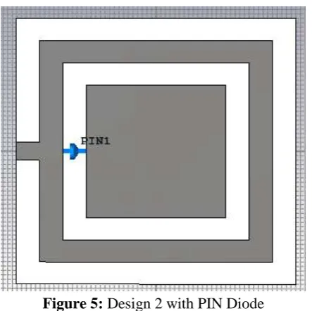
The two separate diagrams are shown for PIN diode’s state. Out of which connection between outer rectangular to inner rectangular is represented with microstrip line with 1mm width represents ON state of diode and provide connection between inner and outer surface. Absence of this connection indicates OFF state of diode.
Simulation results of two different antennas are shows with two different graphs of S11 scattering parameter.
Frequencies below -10dB are considered as usable frequencies and represented with axis markers.
Sr.No. Parameters Dimensions 1 Length of Ground 39.1mm 2 Width of Ground Plane 39.1mm 3 Length of Patch 7.93mm 4 Width of Patch 10.3mm
Figure 2: Design 1 with ON state
Above specified design from Table 1 is implemented using CST Microwave studio in Figure 2. Connecting strip is used as the functionality of ON and OFF state of PIN diode. This design provide S11 Vs Frequency graph
for OFF state and ON state as shown in Figure 3 and 4 respectively.
Figure 3: S11 Vs Frequency graph for OFF state
From the return loss parameter graph S11 for OFF state
frequency of resonance is 9.51 GHz with -19.72 dB
return loss value. The same structure with ON configuration of PIN diode gives 10.41 GHz resonance frequency with -23.79 dB return loss value.
Both these values are in acceptance range of antenna operation with good VSWR value i.e. VSWR less than 1. This structure gives a single band of operation at 9.4 GHz resonance for OFF and ON state. To make this multiband structure we need to cut the structure and add the extra slot inside the main Microstrip (MSA) structure.
Figure 4: S11 Vs Frequency graph for ON state
So to achieve multiband operation considered 30*30mm ground plane and outer slot with 25*25mm dimension on GML substrate with 30*30mm dimensions and cut it with 20*20mm patch, within this rectangular patch is added of dimension 15*15mm.
Figure 5: Design 2 with PIN Diode
Pin diode state can me made ON and OFF depending upon the status of lumped elements of PIN diode.
This design provide S11 Vs Frequency graph for OFF
state and ON state as shown in Figure 6 and 7 respectively.
Figure 6: OFF state S11 scattering parameter
This design provides two usable frequencies (0.349 GHz, 4.449 GHz) in OFF state and four frequencies (0.279 GHz, 1.245 GHz, 4.067 GHz ,and 7.31 GHz).
Figure 7: ON state S11 scattering parameter
III.
RESULT & CONCLUSION
structure. This can be further extended to reduce more inner surface and to provide multiple switching devices to achieve multiband operations.
IV.
REFERENCES
[1] Dimitrios peroulis, Kamal Saraland and Linda P.B.K presents "Design of Reconfigurable Slot antennas," IEEE Transactions on Antennas and Propagation, Vol. 53, N).2, FEBRUARY 2005. [2] Abdelnasser Eldek, Abubaker Abdallah,
Mahmoud Manzou, "Reconfigurable Microstrip Double-Dipole Antennas for Personal Wireless Communications," Wireless Engineering and Technology, 2011, 2, 60-69, April 2011.
[3] S. V. Shynu, G. Augustin, C. K. Aanandan, P.Mohanan, and K. Vasudevan, "Design of Compact reconfigurable dual frequency microstrip antenna using varactor diodes," Progress In Electromagnetics Research,PIER 60, 197–205, 2006.
[4] Huda A. Majid, Mohamad K. A. Rahim*,Mohamad R. Hamid, and Muhammad F. Ismail "Frequency Recongurable Microstrip Patch-Slot Antenna with Directional Radiation Pattern," Progress In Electromagnetics Research, Vol. 144, 319-328, 2014.
[5] Sonia Sharma, Monish Gupta, C.C.Tripathi, "Reconfigurable Antennae: A Review," IJECT Vol.2, Issue 3, Sept. 2011.
[6] Constantine A. Balanis, "Fundamental Parameters of Antennas," in, antenna theory Analysis and design 3rd ed. A JOHN WILEY & SONS, INC., PUBLICATION USA: 2005.
[7] Christos G. Christodoulou, Fellow IEEE, Youssef Tawk, Steven A. Lane, and Scott R. Erwin ,R "econfigurable Antennas for Wireless and Space Applications," Proceedings of the IEEE Vol. 100, No. 7, July 2012.
[8] Mohamad R. Hamid, Mohamad K. A. Rahim, and Muhammad F. Ismail "Frequency Reconfigurable Microstrip Patch-Slot Antenna ," Progress In Electromagnetics Research, Vol. 144, 319-328, 2013.
[9] Pradeep Kumar Neha Thakur Aman Sanghi, "Micro strip Patch Antenna for 2.4 GHZ Wireless Applications," International Journal of
Engineering Trends and Technology (IJETT) – Volume 4 Issue 8- August 2013.
[10] Pei-Yuan Qin, Member, IEEE,Y.Jayguo, Senior Member, IEEE,And Canding, Student Member, IEEE" A Dual-Band Polarization Reconfigurable Antenna For WLAN Systems" IEEE Transactions On Antennas And Propagation, Vol. 61, No. 11, November 2013.
[11] Attan F. Abutarboush,Karim M. Nasr,Hamed Al-Raweshidy, "A Reconfigurable Wideband And Multiband Antenna Using Dual-Patch Elements For Compact Wireless Devices", IEEE Transactions On Antennas And Propagation, Vol. 60, No. 1, January 2012.
[12] Xue-Xia Yang,Atef Z. Elsherbeni,"A Polarization Reconfigurable Patch Antenna With Loop Slots On The Ground Plane", IEEE Antennas And Wireless Propagation Letters, Vol. 11, 2012. [13] Jeen-Sheen Row And Jia-Fu