L E T T E R
Open Access
Ultra-low voltage MEMS switch using a folded
hinge structure
Min-Wu Kim, Yong-Ha Song, Seung-Deok Ko, Sang-Joon Ahn and Jun-Bo Yoon
*Abstract
An ultra-low voltage microelectromechanical system (MEMS) switch for low-power integrated circuit (IC) applications is proposed, fabricated and demonstrated. The folded hinge structure allows a large beam structure to be suspended with a designed air gap, effectively suppressing unwanted deflection. The actuation voltage of the switch was measured to be 1.7 V, the lowest among electrostatic switches. There was no variation in the actuation voltage until 106cyclic actuations, showing the stability of a low actuation voltage in electrostatic actuation for the first time. The contact resistance was around 12Ω, caused by a low contact force below 1μN despite an Au–Au contact.
Keywords:Microelectromechanical system (MEMS) switch; Folded hinge; Actuation voltage; Contact resistance
Introduction
Microelectromechanical/nanoelectromechanical system (M/NEMS) switches have attracted attention as suitable alternatives to metal oxide semiconductor field effect transistors (MOSFETs) owing to their extremely low leakage currents [1,2]. However, the high actuation volt-ages (i.e. pull-in voltage) of mechanical switches have been an obstacle for them to be deployed diversely and widely in real applications. Piezoelectric actuation [3,4] might be one solution to lower the actuation voltage; however, the switching energy of the piezoelectric actu-ation is larger than that of electrostatic actuactu-ation [4]. Moreover, materials exhibiting substantial piezoelectri-city can only be applied.
The actuation voltage for electrostatically actuating mechanical switches is mainly governed by the mechan-ical stiffness of the spring and the size of the air gap. Fabricating mechanical switches with a low stiffness and a thin air gap is challenging because a mechanically compliant structure is subject to bending because of stress and stress gradients in the suspended beam.
We recently reported an electrostatically actuating me-chanical switch that was actuated at 3.0 V, and its applica-tion in mechanical logic gates [5]. Though the actuaapplica-tion voltage is the lowest among electrostatically actuating
MEMS switches, it was still higher than the designed value because of an increased thickness in the air gap, caused by the mechanical stress of the electroplated hinge structure. Here we present an ultra-low voltage mechanical switch actuating at 1.7 V by introducing a folded hinge structure, effectively suppressing the deflection in the compliant hinges. Additionally, the actuation voltage variation during cyclic operations was recorded experimentally with a low actuation voltage level, for the first time.
Findings
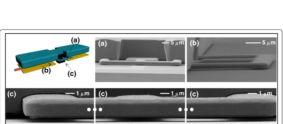
Figure 1(a) shows the original switch with simple hinges. It consists of gate and drain electrodes under a sus-pended beam. To design the switch with a low actuation voltage the hinges should be extremely compliant, which easily results in bending under the influence of material stress, as shown in the inset scanning electron micro-scope (SEM) image in Figure 1(a). In contrast, Figure 1(b) depicts the proposed switch with folded hinges. The folded hinge design is known to be useful for achieving low stiffness [6], high temperature stability [7] and an es-pecially high capability to relieve the stress [8]. In com-parison with the switch with simple hinges, the folded hinge switch showed very little deflection of the sus-pended beam. In the inset in Figure 1(b) are the SEM images. Figure 2 shows magnified SEM images of the folded hinge viewed in different directions. The fabrica-tion process of the proposed switches was the same as that found in the literature [5]. With the folded hinge we
* Correspondence:[email protected]
Department of Electrical Engineering, Korea Advanced Institute of Science and Technology (KAIST), 291 Daehak-ro, Yuseong-gu, Daejeon 305-701, Republic of Korea
100 m 20 m
Gate Drain Top view
-100 m 20 m
Top view
-Gate Drain
Simple hinge
Folded hinge
(a)
(b)
Figure 1Comparison between original and proposed switches. (a)Schematic of the original switch with simple hinges and scanning electron micrograph (SEM) images of the original switch with hinges, bent by material stress.(b)Schematic of the proposed switch with folded hinges and SEM images of the switch with flat folded hinges.
1 m 1 m 1 m
(a)
(b)
(a)
(b)
(c)
(c)
(c)
(c)
5 m 5 m
Figure 2Magnified SEM images of a fabricated folded hinge viewed in different directions. (a)front and(b)side views.(c)highly magnified front view (with air gap).
Kimet al. Micro and Nano Systems Letters2014,2:2 Page 2 of 5
could achieve an air gap thickness as designed (0.45μm) over the entire suspended structure, shown in Figure 3.
The I-V characteristics of the fabricated switch are shown in Figure 4. In this measurement a drain bias of 0.05 V was applied, along with a compliance current of 10μA. The switch was pulled in at 1.7 V (VPI) and stably pulled out at 1.1 V (VPO), building a hysteresis window of 0.6 V. The width of the hysteresis window (|VPI - VPO|) was theoretically calculated [9] as
VPI−VPO
j j ¼FAD⋅
2 gair−gd2
ε0lgatewgateðVPIþVPOÞ; ð 1Þ
whereFADis the adhesion force,ε0is the permittivity of
free space,lgateandwgateare the length and width of the
gate electrode, respectively, gair is the initial air gap
between the beam and bottom electrodes, and gd is
the initial air gap between the dimple and the
bot-tom electrodes. Because VPI and VPO are a function
of lgate, wgate and gair, the width of the hysteresis
win-dow was mainly governed by FAD. FAD is related to
the contact force, that is, if the switch was over-driven then the width of the hysteresis window would increase. As the contact force of the proposed switch
was calculated to be 0.8 μN, which is much smaller
than other electrostatically actuating mechanical swit-ches, there would be little variation of the contact force, and this can lead to comparable hysteresis window (the hysteresis window ultimately limits minimum actuation voltage).
Figure 3SEM images of the fabricated switch showing the designed air gap over the entire suspended beam.
0.0 0.5 1.0 1.5 2.0 2.5
10-15 10-13 10-11 10-9 10-7 10-5
C
u
rr
e
n
t (A
)
Gate Voltage,
V
(V)
I
DI
Figure 4Measured I-V characteristics of the fabricated switch.
The switch was pulled in at 1.7 V and pulled out at 1.0 V.IDandIG
indicates drain and gate current, respectively.
0
1
2
3
4
5
10
-410
-210
010
210
4Int
e
ns
it
y
(
c
ount
/sec)
Depth (nm)
Au
O
C
Although the mechanical contact was accomplished through Au-to-Au, the contact resistance was around 12 Ω, which is much higher than that of the previous switches using Au-to-Au contacts [10,11]. This relatively high contact resistance came from the extremely low contact force of 0.8 μN in theory and 0.46 μN with the finite element method (FEM) simulation, with a gate voltage of 2.0 V. Here, the restoring force and the spring constant of the switches are 0.58 μN and 2.3 N/m, re-spectively. Using the Maxwell–Sharvin contact theory [12], the contact resistance from the respective contact forces should be 2.9 Ω (in theory) and 4.8 Ω(from the FEM simulation). Moreover, there was no significant re-duction in the contact resistance at a higher gate voltage of 4.0 V (higher contact force), which indicates that there were other sources responsible for blocking a per-fect metal-to-metal contact. We analyzed the surfaces of the as-deposited Au films using secondary ion mass spectrometry (SIMS). Figure 5 shows that substantial amounts of carbon and oxygen were observed at a depth of 1 nm. This indicates that an additional film, such as a hydrocarbon film, exists on the surface of the Au film and could not be broken with a gate voltage of 4.0 V.
The contact resistance was much lower in comparison with that in our earlier work [5] (1–2 kΩ) where the contact was formed with Au-to-Ni. A higher contact re-sistance increases the electrical delay in low-power inte-grated circuit (IC) applications. As the mechanical delay of the switches was much larger than the electrical delay, the allowed level for the contact resistance was around several kilo ohms [13,14]. The measured contact resist-ance was far below the ideal level.
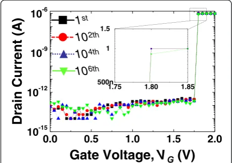
The variation of the actuation voltage during cyclic operations is shown in Figure 6. The switch was repeat-edly actuated with a hot-switching condition of 2.5 μA by biasing the drain voltage to 0.5 V through an external
resistor of 200 kΩ until 106 cycles of operation were completed. There was almost no variation in the actu-ation voltage, showing a stable operactu-ation with a low ac-tuation voltage for the first time. The switch failed by stiction before 107cycles.
Conclusion
A MEMS switch electrostatically actuated at 1.7 V was successfully demonstrated. Introducing folded hinges was the key to achieve the designed air gap in the sus-pended beam with almost no deflection. The contact re-sistance for the fabricated switches was around 12 Ω, which is higher than expected because of an additional film residing on the surface of the contact. This film was mainly composed of carbon and oxygen, identified by SIMS analysis, which is considered as a source for the high contact resistance. The fabricated switches operated well up to 106cycles, without a noticeable change in the actuation voltage. We demonstrated the stability of a low actuation voltage in electrostatic actuation for the first time. To the best of our knowledge, the actuation voltage of 1.7 V is the lowest voltage among electrostatic MEMS switches.
Competing interests
The authors declare that they have no competing interests.
Authors’contributions
MWK carried out design, fabrication, and measurement of the device and drafted the manuscript. YHS performed experimental measurement and analysis of the results. SDK and SJA carried out fabrication of the device. All authors read and approved the final manuscript.
Acknowledgements
This work was supported by the Center for Integrated Smart Sensors funded by the Ministry of Science, ICT & Future Planning as Global Frontier Project (CISS -2012M3A6A6054187).
Received: 7 February 2014 Accepted: 28 April 2014
References
1. Chen F, Spencer M, Nathanael R, Wang C, Fariborzi H, Gupta A, Kam H, Pott V, Jeon J, Liu TJK, Markovic D, Stojanovic V, Alon E (2010) Demonstration of integrated micro-electro-mechanical (MEM) switch circuits for VLSI applications. IEEE ISSCC 150–151
2. Lee JO, Song YH, Kim MW, Kang MH, Oh JS, Yang HH, Yoon JB (2013) A sub-1-volt nanoelectromechanical switching device. Nat Nanotech 8:36–40 3. Proie RM Jr, Polcawich RG, Pulskamp JS, Ivanov T, Zaghloul M (2011)
Development of a PZT MEMS switch architecture for low-power digital applications. J Microelectromech Syst 20:1032–42
4. Lee HC, Park JY, Bu JU (2005) Piezoelectrically actuated RF MEMS DC contact switches with low voltage operation. IEEE Microw Compon Lett 15:202–4
5. Kim MW, Song YH, Yang HH, Yoon JB (2013) An ultra-low voltage MEMS switch using stiction-recovery actuation. J Micromech Microeng 23, doi:10.1088/0960-1317/23/4/045022
6. Kim JM, Park JH, Baek CW, Kim YK (2004) The SiOG-basedsingle-crystalline silicon (SCS) RF MEMS switch with uniform characteristics. J Microelectromech Syst 13:1036–42
7. Nguyen CTC (1998) Micromachining technologies for miniaturized communication devices. Proc SPIE 3514:24–38
8. Tang WC, Nguyen TCH, Howe RT (1989) Laterally driven polysilicon resonant microstructures. Sens Actuators 20:25–32
0.0 0.5 1.0 1.5 2.0
10-15 10-12 10-9 10-6
Drain Current (
A
)
Gate Voltage,
V
(V)
1.75 1.80 1.85 500n 1 1.5
1
st10
2th10
4th10
6thFigure 6Variation of the actuation voltage during cyclic actuations.
Kimet al. Micro and Nano Systems Letters2014,2:2 Page 4 of 5
9. Ko SD, Lee JO, Yang HH, Kim MW, Song YH, Yoon JB (2011) An insulating liquid environment for reducing adhesion in a microelectromechanical system. Appl Phys Lett 99, 113516 http://dx.doi.org/+10.1063/1.3640228 10. Majumder S, McGruer NE, Adams GG, Zavracky PM, Morrison RH, Krim J
(2001) Study of contacts in an electrostatically actuated microswitch. Sens Actuators A 93:19–26
11. Kwon H, Jang SS, Park YJ, Kim TK, Kim YD, Nam HJ, Joo YC (2008) Investigation of the electrical contact behaviors in Au-to-Au thin-film contacts for RF MEMS switches. J Micromech Microeng 18, doi:10.1088/0960-1317/23/4/045022
12. Ke F, Miao J, Oberhammer J (2008) A ruthenium-based multimetalcontact RF MEMS switch with a corrugated diaphragm. J Microelectromech Syst 17:1447–59
13. Knoll AW, Grogg D, Despont M, Duerig U (2012) Fundamental scaling properties of electro-mechanical switches. New J Phys 14:123007, doi:10.1088/1367-2630/14/12/123007
14. Kam H, Liu TJK, Stojanovic V, Markovic D, Alon E (2011) Design, optimization, and scaling of MEM relays for ultra-low-power digital logic. IEEE Trans Electron Devices 58:236–250
doi:10.1186/s40486-014-0002-y
Cite this article as:Kimet al.:Ultra-low voltage MEMS switch using a folded hinge structure.Micro and Nano Systems Letters20142:2.
Submit your manuscript to a
journal and benefi t from:
7Convenient online submission
7Rigorous peer review
7Immediate publication on acceptance
7Open access: articles freely available online
7High visibility within the fi eld
7Retaining the copyright to your article