Copyright © 2013 IJECCE, All right reserved
Capacitance Measurement Methods for Integrated
Sensor Applications
Alireza Hassanzadeh, Robert G. Lindquist
Abstract – In this paper different measurement methods that have been used for integrated capacitance measurement are reviewed and their advantage and disadvantages are discussed. For the designers of high accuracy on chip integrated circuits for capacitive sensors, it is important to know which method will provide the best approach for high accuracy, small chip area and power consumption especially for array sensors. These methods include on chip capacitive sensor and transducer measurement techniques that have been implemented for low value capacitance evaluations using CMOS technology. After the best structure is known the designer can optimize the chip for specific application. Voltage mode and current mode, linear and switched mode techniques are reviewed and a useful comparison table comparing all figures of merit including accuracy, range of measurement, chip area, speed and complexity is provided. The provided comparison table can be used as a reference for analog designers in the design of high accuracy integrated capacitive sensor interface.
Keywords – CMOS Interface Circuit, Capacitive Sensor, Sensor Integration, Capacitance Measurement, System on a Chip.
I. I
NTRODUCTIONCapacitive measurement techniques have been developed through years and many techniques have been presented even in textbooks [1-3]. Recent advances in MEMS and integration of sensor devices with interface circuitry has demanded for integrated measurement methods that can push the accuracy and resolution limits of the measurement. MEMS accelerometer, capacitive tomography, particle detectors, lab-on-chip systems are some examples of these systems. Because of stray and cable capacitances it is hard to measure capacitance in the range of Atto and Femto Farads on discrete systems. Integration reduces parasitic capacitance and increases system resolution. Some high accuracy accelerometers would not be possible without integrated circuit implementation. CMOS technology is an inexpensive and promising technology for integrated sensor applications. Most interface circuit designs have been developed using voltage mode signal processing and some used current mode implementations. Current mode signal processing does not need high voltage swing and can be used for low voltage applications. Accuracy of current mirrors limits these kinds of circuit applications.
Previous work in reference [1] introduces low power capacitive sensor interface design using CMOS circuits that mostly focus on switched capacitor and sigma-delta technique implementation and does not review all reported techniques for capacitance measurement. Reference [2] reviews different capacitance electrode for sensor configuration and basic principles of capacitance
measurement techniques. Impedance matching and some applications are discussed but it does not focus on CMOS implementation. Recently published journal paper in [3] has reviewed CMOS capacitive sensors for lab-on-chip applications, and its main focus is on the general system design including electrodes and micro fluidic implementation problems in CMOS technology. It does not provide a comparison of methods and the circuit part is focused on CBCM (Charge Based Capacitance Measurement) technique and not all previously reported methods.
In this paper different capacitance measurement techniques for integrated CMOS implementation are reviewed and their limitations and resolution are discussed. A useful comparison table is provided that gives a general view for circuit designers to choose from different techniques based on the required accuracy and complexity. This paper is arranged as follows. First different CMOS integrated voltage and current mode techniques and their principle of operation are discussed. A comparison of measurement merits is provided afterward. The conclusion remarks are at the end.
II. I
NTEGRATEDC
APACITANCEM
EASUREMENTT
ECHNIQUESIn this section different CMOS circuits reported for capacitive sensor interface are reviewed. The most common and easy to design method for implementing capacitance measurement is charge and discharge method. The voltage developed across a capacitance is proportional to the charging current. The larger the capacitor the longer it takes to charge with constant current. Since the time can easily be measured using a simple counter, digital output is easily available. This method actually is a capacitance to time duration converter. By using a voltage comparator, it is possible to convert the voltage ramp into a pulse width. The pulse width is proportional to capacitance value. This method has been used for array of DNA sensor integrated system [4]. The block diagram of the system is shown in figure 1.
Copyright © 2013 IJECCE, All right reserved using this method. The range of reported measurement is
from 330pF to 10nF with 1% error. The advantage of this method is its simplicity and direct digital output besides small chip area. It has been used for an array of 128 DNA sensors.
Fig.1. Charge discharge method block diagram [4] For smaller capacitance range, such as capacitance of interconnection wires in an integrated circuits, a method called Charge Based Capacitance Measurement (CBCM) has been introduced [5]. Two identical CMOS inverters have been used to provide a differential measurement. One inverter is dummy and the output of the other inverter is connected to the unknown capacitor between two wires A and B, as shown in figure 2. These two inverters are excited using pulses Vp and Vn, in a way that PMOS and NMOS transistors are not ON at the same time. Therefore, the capacitance at the output node of the inverters is charged to the supply voltage via PMOS transistor and discharged via NMOS transistor alternatively. The average current pulled from the supply voltage ( I , 'I ) is proportional to the capacitance value at the inverter output node. By using an analog current meter, it is possible to measure the average current difference that is proportional to the unknown capacitance. Since differential measurement has been used, all transistor and layout parasitic capacitances will be canceled out and the current difference is only proportional to the load capacitance at node P. This method has also been used for lab-on-chip applications for array of sensors [6]. Figure 2 shows the basic schematic of CBCM method.
Fig.2. CBCM method principle [5]
External analog current meters can be used for the difference current measurement. In contrast, current mirrors can be used to produce difference current on chip, which usually reduces the accuracy, because of mismatch problems. Range of measurement of this method has been reported as 20fF with 10aF resolutions. The disadvantage of this method is limited range of measurement and using current mirrors that usually do not provide good matching [7-11].
Using the idea of differential measurement and charge transfer, a method has been developed that is capable of doing differential, absolute and ratio metric capacitance measurement. The block diagram of this method has been shown in figure 3. Using analog switches and four arm capacitors C1 to C4, unknown capacitor can be evaluated. In the first phase, S1 and S4 are closed and the capacitors are charged to the supply voltage. In the second phase, S2 and S4 are closed and capacitors are connected to the source of the four transistors. Because of low impedance of the source, parasitic capacitances will be cancelled out. The charge difference between these capacitors are transferred and sampled on C5 to C8 capacitors. The offset inputs can be used for offset adjustment or to provide negative feedback from OTA. This method is called charge transfer method in a closed loop configuration. Since differential method has been used, parasitic capacitances are canceled out and the only problem would be providing matched capacitors that are easily implemented on integrated circuits [12]. This method has a 66dB dynamic range and minimum sensitivity to CMOS process variation. Sensitivity of this work has been reported to be 1.56mV/fF with maximum of 640fF measurement range [12].
Adding switches to circuit usually adds more problems such as charge injection and offsets. To avoid charge injection some all-analog methods have been developed. Many linear charge amplifiers have been reported in the literature for capacitance measurement. These linear circuits normally need analog offset and gain adjustments [29]. Synchronous detection or lock-in detection technique uses all continuous time signal processing to measure the capacitor value. In this method capacitance value is modulated with a known signal, and after amplification using synchronous demodulation the original signal will be retrieved. In this method, low frequency noise, DC offset and other off-band signals will be modulated to higher frequencies.
Copyright © 2013 IJECCE, All right reserved The original signal will be demodulated and restored
using a low pass filter at the output. Although demodulator adds some complexity to the circuit such as non-linearity and offset compensation, still has very high resolution. Because this method does not use switches, charge injection will not cause problem. Very high sensitivities have been reported using this method. Figure 4 shows block diagram of such a system [13].
Fig.4. Lock in detection method [13]
A square wave signal is applied to the capacitors and the output signal is amplified using a differential charge amplifier. Input and output common mode feedback have been used to stabilize DC biasing. After amplifier, a demodulator and low pass filter will provide the DC output signal, which is proportional to the capacitance difference. Sensitivity of 26.5aF in 0.44pF range with 81dB dynamic range has been reported for this method [13]. This method also has been used in reference [14] using BiCMOS process that utilizes analog multiplier instead of switched demodulators to achieve higher sensitivity of the measurement. Similar techniques have been used in other papers [15-18].
A group of techniques have been developed known as current mode circuits that process the signal in current instead of voltage. Block diagram of a simple current mode method for capacitance measurement is shown in figure 5. A current source is used to excite two capacitors and the output current is differentially amplified using differential current amplifier.
Fig.5. Simple current mode technique block diagram [19] Current mode signal processing does not need large voltage swing therefore it can be used for low voltage applications. A current mode implementation of sensor capacitance change measurement is shown in figure 6. Differential capacitors are excited using a triangular waveform and instead of voltage amplifier current amplifier has been used to amplify the sensor signal. All offset canceling and other signal processing are done in current mode [18]. The current output of the CA is added to the current IB and ID to charge capacitor C. The triangular excitation waveform is synchronized with the clock signal. The switches SA1 and SA2 change the
polarity of the signals to charge and discharge capacitor C in each half cycle of the clock period. The current
I
B is larger than IDmaxICA to make the circuit operate properly. The waveforms of the circuit operation are shown in figure 6. In the first half cycle of the clock period, the capacitor C is charged and in the second half of the clock period the switches SA1 and SA2 change polarity and the capacitor starts to discharge. As the capacitor voltage C becomes negative the comparator output changes state. The output pulse width is proportional to the capacitance difference.Fig.6. Current mode capacitance to pulse width converter [18]
Another current mode dual slope method implemented in BiCMOS technology is shown in figure 7. Three integrators have been implemented using OTAs. A reference capacitance C on the feedback loop of G1 isR charged using a reference currentIRMP. The unknown capacitance CX is in the feedback loop of G2 integrator. The feedback loop of G3 makes VRMP VX and as a result
2 1 I
I . The current ISHis a reference current that is subtracted from I2 and the difference current is used to charge feedback capacitanceC , on G4 OTA. AfterI integrating phase, the input current is disconnected using S3 and discharge current IDIS via S4 discharges the integrating capacitor C . The output voltage of G3 goes toI the comparator that produces a pulse with duration proportional to the unknown capacitance value. Range of reported measurement is 0.88-1.2pF [20]. The parasitic capacitances of the sensor are compensated using low impedance nodes of G2 OTA.
Copyright © 2013 IJECCE, All right reserved Fig.7. Current mode dual slope capacitance measurement
with digital output signal [20]
Fig.8. switched capacitor measurement [21] The principle of operation is to integrate the charge difference between an unknown and a reference capacitor. The charge difference between these two capacitors is integrated on a feedback capacitor. The output voltage of the integrator is proportional to the capacitance difference. Sensor capacitors are CSnand reference capacitors are
m
Cref that can be selected using analog switches for different ranges. In order to avoid capacitor Cf1saturation, a switch discharges the integrating capacitor frequently. Series dummy switches have been used to reduce charge injection. The second charge amplifier stage has been used
for variable gain implementation using ф3-ф6 switches
andCg1,2capacitors. In addition, parallel parasitic capacitances are also canceled because of low impedance input of the OpAmp. By using switched capacitor techniques, there will be no need for high value resistors in a feedback loop to bias the amplifier. This resistor has effect on frequency response of the amplifier. Furthermore, DC offset cancellation can be achieved easily using auto zero techniques. Besides these advantages switched capacitor circuit can be followed by a sigma-delta analog to digital converter that is not sensitive to process and does not need accurate components for high accuracy A/D conversion.
A more complete technique that uses differential technique and CDS for offset cancellation is shown in figure 9. This technique has been used for a micro gravity MEMS accelerometer. The measurement system uses a bridge configuration consisting of sensor and reference capacitors. The difference signal is amplified using a two phase switched capacitor charge amplifier that uses CDS capacitors for offset cancellation. Amplifier output signal
is sampled on a sample and hold buffer to go to A/D converter. This method has been used for a high accuracy accelerometer in [28].
Fig.9. Differential switched capacitor MEMS accelerometer interface [28]
There are many other reported techniques in the literature for integrated capacitance measurement that are mostly derivative of the above-mentioned methods. In the next section these techniques are compared for different figures of merit.
III. C
OMPARISON OF THE TECHNIQUESCopyright © 2013 IJECCE, All right reserved
Table-1- Comparison of different capacitance measurement methods
Resolution Accuracy Range Speed
1 Lock-in (~0.1aF) Switched Cap.(0.01%) Charge Discharge (~100p-10nF)
Current Mode Differential (~500ns)
2 CBCM (~10aF) Lock-in Switched Cap.(~p-nF) CBCM (~10μs)
3 Switched Cap. (~0.1fF) CBCM (~0.5%) Current Mode Differential (~pF)
Lock-in (~20μs)
4 Charge Transfer (0.5fF) Current Mode Dual Slope (~0.6%)
Current Mode Dual Slope (~1.2pF)
Current Mode Dual Slope (~50μs)
5 Current Mode Dual Slope (~0.9fF)
Charge Discharge (~1%) Charge Transfer (~0.8pF) Switched Cap. (~100μs-ms)
6 Current Mode Differential (~1fF)
Charge Transfer (~2%) Lock-in (~150fF) Charge Transfer (~200μs)
7 Charge Discharge (~pF) Current Mode Differential (~2.5%)
CBCM (20fF) Charge Discharge (~ms)
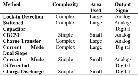
Table 2: Complexity, chip area and output signal type of methods
Method Complexity Area Used
Output Signal Lock-in Detection Complex Large Analog Switched
Capacitor
Complex Large Analog/ Digital
CBCM Simple Small Analog
Charge Transfer Complex Large Analog Current Mode
Dual Slope
Complex Large Digital
Current Mode Differential
Simple Small Analog/ Digital Charge Discharge Simple Small Digital
IV
.
CONCLUSIONThe growing area of on-chip capacitive sensor integration, demands for a good review paper that introduces different CMOS implementations and comparison of the methods for designers. In this paper different methods for integrated capacitance measurement were presented and their advantages and disadvantages were discussed. The comparison table provided will give a quick decision making aid for the range of measurement and accuracy of the techniques.
R
EFERENCES[1] R. Puers, C.V.Hoof, “Ultra low power capacitive sensor interface” Springer 2007.
[2] Capacitive sensors design and applications, L.K. Baxter, IEEE press 1997.
[3] CMOS capacitive sensors for lab on chip applications: A multidisciplinary approach, E.Ghafarzadeh, M.Sawan,Analog circuits and signal processing, 2010.
[4] C. Stagni, C. Guiducci, S. Carrara, ”CMOS DNA Sensor Array With Integrated A/D Conversion Based on Label-Free Capacitance Measurement “, IEEE JSSC 2006.
[5] N. D. Arora, L. Song,“Atto-Farad Measurement and Modeling of On-Chip Coupling Capacitance”, IEEE Electron device letters 2004.
[6] E. Ghafar-Zadeh, M. Sawan, “A Core-CBCM sigma delta capacitive sensor array dedicated to lab-on-chip applications”, Sensor and Actuator A, Elsevier 2008.
[7] D. Sylvester,J.C.Chen, C. Hu, “Investigation of interconnection capacitance characterization using charge based capacitance measurement CBCM technique and three dimensional simulation”, IEEE Journal of solid state circuits 1998.
[8] E. Ghafarzadeh, M. Swan, “Charge based capacitive sensor array for CMOS based laboratory on chip applications”, IEEE Sensors
Journal 2008.
[9] I. Evans, T. York, “Microelectronic capacitance transducer for particle detection”, IEEE Sensors journal 2004.
[10] L. Vendrame, L.Bortesi, A.Bogliolo,”Accuracy and improvement of on chip charge based capacitance measurement”, University of Urbino Italy.
[11] Y. Wen Chang, T.Lu, Y. King, ..”Charge based capacitance measurement for bias dependent capacitance ”, IEEE Electron device letters, 2006.
[12] P.D.Dimitropoulos, D.P.Karampatzakis, ”A Low-Power/Low-Noise Readout Circuit for Integrated Capacitive Sensors”, IEEE Sensor Journal 2006.
[13] M.Suster, J.Guo,”Low-noise CMOS integrated sensing electronics for capacitive MEMS strain sensors”, IEEE CICC, 2004.
[14] M.Tavakoli, R. Sarpeshkar, “An offset canceling low noise lock in architecture for capacitive sensing”, IEEE JSSC 2003. [15] J.Xu, G. Meynants, P. Merken, “Low power lock in amplifier for
complex impedance measurement”, IEEE 2009.
[16] M.Lemkin,Bernhard E.Boser,”A three axis micromachined accelerometer with a CMOS position sense interface and digital offset trim”, IEEE Journal of solid state circuits, 1999.
[17] A.Burstein, W.J.Kaiser, “Mixed analog digital highly sensitive sensor interface circuit for low cost microsensors”, Intl. Conf. Solid state sensors and actuators 1995.
[18] P.Bruschi,N.Nizza,M.Dei, G.Borillaro, “A low power capaci-tance to pulse width converter for integrated sensor”,IEEE 2007. [19] S.Pennisi, “High performance and simple CMOS interface circuit for differential capacitive sensors”, IEEE circuit and system 2005.
[20] P. Bruschi, N. Nizza, M.Piotto, “A current mode dual slope integrated capacitance to pulse duration converter”, IEEE Journal of solid state circuits 2007.
[21] N.Yazdi, A.Mason, “A generic interface chip for capacitive sensors in low power multi parameter micro systems”, Elsevier Sensor and actuators 1999.
[22] K.Kondo,K.Watanabe, “A switched capacitor interface for capacitive sensor with wide dynamic range”, IEEE Trans. on Instrumentation and measurement 1989.
[23] B.Wang, T.Kajita,T.Sun, “High accuracy circuits for on chip capacitive ratio testing and sensor readout”, IEEE Trans. on instrumentation and measurement 1998.
[24] C.Leme, T.Boltshauser, H.Baltes, “CMOS absolute value precision capacitance measurement system”, IEEE 1992. [25] M.Yamada,K.Watanabe, “A capacitive pressure sensor interface
using over sampling delta sigma modulation technique”, IEEE Trans. on instrumentation and measurement 1997.
[26] M.Bingesser, T.Loeliger,W.Hinn,…,”Low noise sigma delta capacitance to digital converter for sub pF capacitance sensor with integrateddielectric loss measurement ”, EDAA 2008. [27] S. Ogawa, K. Wtanabe, “A switched capacitor interface for high
accuracy high speed ratiometric signal processing of differential capacitance transducers”, IEEE Inst. And measurement, 2001. [28] B.V.Amini, “AMixed-Signal Low-Noise Sigma-Delta Interface
Copyright © 2013 IJECCE, All right reserved
[29] R.R.Harrison, C. Charles, “A Low Power Low Noise CMOS Amplifier For Neural Recording Applications”,IEEE Journal Of Solid States Circuits 2003.
A
UTHOR’
SP
ROFILEAlireza Hassanzadeh
was born in 1973 in Tehran, Iran. He received his B.S. degree in electronic engineering in 1996 and his M.Sc. in 1999 from Iran University of Science and Technology (IUST). He also received his M.Sc. and Ph.D. in electrical engineering from the University of Alabama in Huntsville, USA in 2008 and 2011 respectively. He is now with the Shahid Beheshti University, Tehran, Iran. His research interests are analog and mixed signal and low power sensor interface systems. He is a member of Phi-Kappa-Phi, Eta-Kappa-Nu honor societies.
![Fig.5. Simple current mode technique block diagram [19]](https://thumb-us.123doks.com/thumbv2/123dok_us/8789300.1765694/3.595.78.263.517.607/fig-simple-current-mode-technique-block-diagram.webp)
![Fig.9. Differential switched capacitor MEMSaccelerometer interface [28]](https://thumb-us.123doks.com/thumbv2/123dok_us/8789300.1765694/4.595.57.289.35.270/fig-differential-switched-capacitor-memsaccelerometer-interface.webp)