Novel Control Techniques of Input-Match and
Output-Match for an Inductively Degenerated
Low Noise Amplifier
Sami Mahersi, Hassene Mnif, and Mourad Loulou
National Engineering School of Sfax/ Department of Electrical Engineering, Sfax, Tunisia Email: [email protected], { hassene.mnif, mourad.loulou}@ieee.org
Abstract—This paper presents two novel techniques to
control the input match and the output match for 2.45 GHz CMOS inductively degenerated Low Noise Amplifier (LNA). These control techniques allow the compensation of all deviation of these parameters caused by the undesirable factors such as Process-Temperature-Voltage (PVT) variations, parasitic elements, etc. These techniques are studied theoretically and through simulation to be validated. Moreover, we investigated the effects of the parameters tuning in the other LNA performances and we showed that these effects are not important. The simulation results present a control of the input match S11 between -33.12dB and -56.23dB. The input match center frequency can be controlled between 2.361GHz and 2.603GHz. The tuning of the output match S22 can be made between -17.98dB and -53.65dB. The center frequency of the output match can be controlled between 2.336GHz and 2.540GHz. Also, we proved that the control of the input match quality and its center frequency are independent. The same result was shown for the output match quality and its center frequency.
Index Terms—low noise amplifier, control, input match,
output match, resonance frequency
I. INTRODUCTION
In recent years, a lot of research has been focused on the challenge of Radio Frequency Integrated Circuits (RFIC) regarding their integration level to achieve low cost and low power consumption circuits. In the future, the CMOS technologies (lower than 90 nm) will integrate on-chip complex analog / RF /digital circuits [1]. However, this complicates the Systems-On-Chip (SOC) and their test becomes difficult and expensive. Moreover, the test equipments are very expensive for SOCs, especially, when they are complicated. In addition, each performance test needs a different stimulus and test configuration. Therefore, the per-chip test time becomes long and needs an expensive automatic test equipment (ATE). For example, the tests for the noise figure and the third-order intercept point need significantly different tests setups [2]. Moreover, the chip manufacturers are facing a new
Manuscript received May 3, 2013; revised July 26, 2013
challenge in precisely predicting the variation devices, process skew, and mismatch [3]. Therefore, the product becomes costly. On the other hand, the chip test is very necessary after the circuit manufacture as well as during the RF device operation. This is because the RF circuits are exposed to many adverse factors, such as; transistor corner variation (ff, tt, ss), bond wire inductance variation, on-chip capacitance and inductance variation (min, typ, max), temperature variation [3], [4], power supply variation, parasitic elements and process variations, leading to the degradation of the circuit performances. Therefore, the RF device operates badly. These process variations become an important problem with technology scaling. Especially, for the RF circuits that operate at GHz frequencies, such variations can considerably change the circuit performance [5].
In the radio frequency reception chain, the Low Noise Amplifier (LNA) is considered as one of the most critical RF blocs. It might also be exposed to these undesirable factors that affect the LNA parameters (Gain, input match, output match, noise figure and linearity). In this paper, we proposed tow novel techniques to control some critical performances of an inductively degenerated [6], [7] LNA, such as the input match quality and its center frequency and the output match quality and its center frequency. These control techniques are exploited to compensate all operation frequency deviations and to better the quality of the input and the output matches when they are degraded. These techniques might be very useful in the self calibration system of the input and output match of the LNA, as well.
The effectiveness of these techniques are demonstrated theoretically and by simulations for an LNA operated at the center frequency of 2.45GHz in the 2.4GHz-2.485GHz frequency band.
II. INPUT MATCH AND OUTPUT MATCH CONTROL
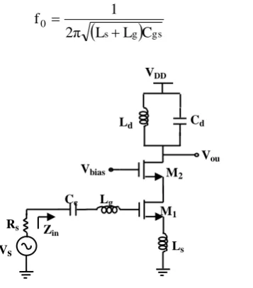
We are basically used to the topology of the common-source inductive degeneration LNA. The scheme of this LNA is shown in Fig .1.
As has been proven in [6], the input impedance can be written as follows:
gs s m gs g s in
C L g ωC
1 L L ω j
Z
(1)
At the resonance frequency, the input impedance becomes equal to its real part as shown in (2):
gs s m in
C L g
Z (2)
The expression of the resonance frequency f0 is
obtained when the imaginary part is equal to zero; it is given by:
s g
gs0
C L L 2π
1 f
(3)
Figure 1. Common-source inductive degeneration LNA circuit.
Equation (2) shows that the input match quality can be tuned when Cgs, Ls, or gm is varied. On the other hand,
equation (3) shows that the resonance frequency control can be made when we adjust Cgs, Lg or Ls. In Ref. [8], the
authors proposed a control approach of the input match by adjusting the inductance Lg. The major issue of this
technique is the complication in the variable inductance implementation. As an alternative for this method, we can tune the input mach quality by means of the transconductance gm. However, gm can alter the gain,
linearity and noise figure of the LNA. Then, the elements Lg, gm and Ls cannot be used to tune the input match quality
and the resonance frequency.
Concerning the output matching, in Ref. [9], the authors proposed an approach to control the output match S22 for
an inductively degenerated LNA, consisting of tuning the load capacitance placed between the drain of the transistor
M2 and the ground. In this work, the impact of the control
is investigated only on the gain and the input match. In this paper, however, we propose two novel techniques:
The first technique permits to control the input match quality and its center frequency. Our main idea was to introduce two variable capacitors Cs and Cg that are used to
independently tune both the quality of the input match and its center frequency respectively as shown in Fig. 2.
The second technique allows to control the output match quality and its center frequency. The idea was to introduce a variable resistance Rtune and a variable
capacitance Ctune located in series between the cascode
transistor drain M2 and the load impedance RL to control
the output match quality and its center frequency respectively as shown in Fig. 2.
Figure 2. LNA scheme with the control elements Cs, Cg, Rtune and Ctune .
A. Input Match Quality and Its Center Frequency Control Technique
From Fig. 2, the expression of the input impedance is given by (4):
2 s s
gs s m tots s 2
s g in
C C L ω 1
L g ωC
1 C L ω 1
ωL ωL
j Z
(4)
where Ctot is the equivalent capacitance of the association
in series of Cg and Cgs, it is expressed by:
gs g
tot C
1 C
1 C
1
(5)
Equation (4) shows that the real part of the input impedance depends on Cs and not on Cg. Then, when we
tune the input match center frequency by sweeping Cg, the
input match quality is not influenced. The technique proposed in Ref. [10] uses a variable capacitance Cd in
parallel with Cgs to control the input match center
frequency and a variable capacitance Cs in parallel with the
inductance Ls to tune the input match quality. Nevertheless,
the input match quality can be affected when Cd varies.
To obtain the resonance frequency expression, we take the input impedance imaginary part equal to zero. We find
VDD
Vou
t
Ls
Lg
M1
M2
Ld Cd
Rs
Vs Zin
Vbias
Cc
four solutions; two negative solutions that are discarded and two positive solutions that are given by (6):
tot s s g tot g s g s s h
l, 0,
C C L L
Δ C
L 1 C L
1 C L
1
2 1
ω
(6)
where
LgCtot LsCtot LsCs
2 4
LgLsCsCtot
Δ (7)
Equation (6) indicates a lower frequencyω0,land a
higher frequencyω0,h. The system of equations formed by
the input impedance real part equal to 50Ω and the higher resonance frequency equal to 2.45GHz does not admit solutions. Thus, the higher frequency ω0,h is rejected.
The used resonance frequency is given by (8):
tot s s g tot g s g s s 0
C C L L
Δ C
L 1 C L
1 C L
1
2 2π
1
f
(8)
The elements Ctot, Cs, Lg and Ls are sized to provide
2.45GHz center frequency associated with 2.4 – 2.485GHz band and an input match equal to 50Ω.
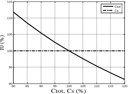
Fig. 3 shows the curves of the resonance frequency f0
versus the two capacitances Ctot and Cs. It is clear that the
resonance frequency depends greatly on Ctot and very
faintly on Cs. Thus, Ctot is a fine mean to control the input
match center frequency. Furthermore, the control of the input match quality by Cs does not affect the center
frequency of the input match.
80 85 90 95 100 105 110 115 120
90 95 100 105 110 115
Ctot, Cs (%)
f0
(%
)
Ctot Cs
Figure 3. The plots of the resonance frequency f0 versus the two capacitances Ctot and Cs.
At the resonance frequency, the input impedance is equal to the real part and it is expressed by:
02 s s
gs s m inω0 in,
C C L ω 1
L g )
Real(Z Z
(9)
Equation (9) indicates that the input impedance depends on gm, Ls, Cgs. Fig. 4(a), Fig. 4(b) and Fig. 4(c) present
respectively the curves of the input impedance real part versus Cs for different values of gm, Ls and Cgs.
200 400 600 800 1000 1200 1400 1600 1800 2000
40 45 50 55 60 65 70
Cs (fF)
R
e
a
l(Z
in
)
(O
h
m
)
gm = 10e-3 A/V gm = 60e-3 A/V gm = 30e-3 A/V
(a)
500 1000 1500 2000 2500 3000
44 46 48 50 52 54 56 58
Cs (fF)
R
e
a
l(Z
in
)
(O
h
m
)
Ls = 0.30nH Ls = 0.32nH Ls = 0.31nH
(b)
200 400 600 800 1000 1200 1400 1600 1800 2000
44 46 48 50 52 54 56 58
Cs (fF)
R
ea
l(Z
in
) (
O
hm
)
Cgs = 100fF Cgs = 300fF Cgs = 200fF
(c)
Figure 4. Input impedance Curves versus the capacitance Cs (Cs start from 10fF):
(a) for different values of gm. (b) for different values of Ls. (c) for different values of Cgs.
Fig. 4(a), Fig. 4(b) and Fig. 4(c) indicate that the control range of the input match quality using Cs depends on gm, Ls
and Cgs respectively. This range becomes wider if Ls
decreases, gm lessens or Cgs increases.
B. Output Match Quality and Its Center Frequency Control Technique
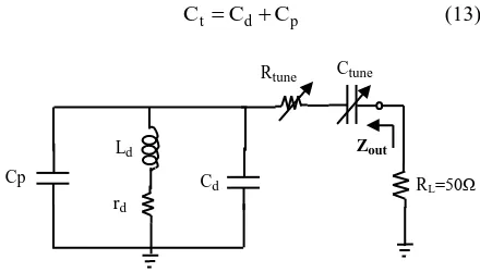
The scheme of the output matching network of the LNA is presented in the Fig. 5. The LNA output impedance Zout
is composed of the control elements Rtune and Ctune, a load
capacitance Cd, a load inductance Ld in series with the load
the cascode structure constituted of the transistors M1 and
M2. The output impedance is given by (10):
) jImag(Z )
Real(Z
Zout out out (10)
where the Real(Zout) and the Imag(Zout) are respectively the
real and imaginary part, given by (11) and (12) respectively.
2t d 2 d t 2
d tune
out
C r ω L C ω 1
r R
) Real(Z
(11)
2 t d
2
d t
2 tune t2 d d t 2 d out
C ω
1
C r ω L C ω 1
C r ω L C ω 1 ωL )
Imag(Z
(12)
where Ctis the equivalent capacitance of the association in parallel of Cd and Cp. It is given by (13):
p d
t C C
C (13)
Figure 5. Output matching network Schematic.
The resonance frequency is obtained when the imaginary part is equal to zero. This results in four solutions; two positive solutions that are expressed by (14) and two negative solutions that are discarded:
2α δ β ,
ωrl,h (14)
where α, β, δ are given by (15), (16) and (17) respectively.
2 d t 2 d ttuneCL CL
C
α (15)
2t d d t 2 d t d
tuneL C r 2CL r C
C
β (16)
λ α 4 β
δ 2 (17)
where λ is equal to:
1
λ (18)
Equation (14) indicates a higher frequency ωr,h and a lower frequency ωr,l. The system of equations formed by the output impedance real part equal to 50Ω and the higher resonance frequency equal to 2.45GHz does not admit solutions. Then, the higher frequency ωr,h is rejected. The used resonance frequency is given by (19):
2α δ β π 2
1 fr
(19)
The elements of the output matching network Rtune, Ctune,
Cd, Ld and rd are sized to have an output match 50Ω at
2.45GHz operation frequency.
Equation (11) shows that the output impedance real part depends only on the control element Rtune. On the other
hand, equation (12) indicates that the output impedance imaginary part depends only on the control element Ctune.
Then, the resonance frequency depends on Ctune and not on
Rtune. Accordingly, the control of the output match center
frequency using Ctune has no effect on the output match
quality and the output match quality control using Rtune
doesn’t affect the center frequency of the output match. Then, the tunings of the output match quality and its center frequency are performed separately.
III. TECHNIQUES VALIDATION
In this part, we validated the proposed control techniques through simulation. We sized the LNA taking into account the control elements. The nominal values of these elements are determined in order to ensure an input and output match of 50Ω at 2.45GHz operation frequency. The LNA simulation is performed using 0.35µm CMOS technology. The circuit parameters at 2.45 GHz using nominal values of Cs, Cg, Rtune and Ctune are shown in Table
I.
TABLE I. LNAPARAMETERS AT 2.45GHZ
Parameters Value
S21 (dB) 19.80
S11 (dB) -56.23
Real(Zin) (Ω) 50.15
S22 (dB) -53.65
Real (Zout) (Ω) 49.80
NF (dB) 1.93
CP1 (dBm) -21.43
A. Controlling the Input Match Quality
The capacitance Cs is swept around the nominal value
1000fF in the range of [10fF – 2000fF].
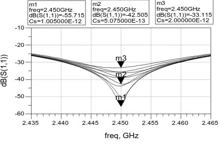
Fig. 6 shows the control of the input match S11 at
2.45GHz operation frequency by Cs. This control can be
achieved between -33.12dB and -56.23dB. Then, for an input match quality alteration due to the undesirable factors, S11 can be calibrated until 23.11dB approximately.
Also, it can be seen that the input match S11 reaches the
lowest value at 2.45GHz when Cs tends to 1000fF. Fig. 7
shows the tuning of the real part of input impedance around 50Ω at 2.45GHz by Cs.
On the other hand, the study of the impact of the input match quality control on the other LNA parameters is necessary. Table II shows that the sweeping of Cs to tune
the input match quality has no significant impact on the RL=50Ω
Ld
Cd
Cp
Rtune Ctune
Zout
rd
other parameters of the LNA: the gain, output match, noise figure and linearity.
2.440 2.445 2.450 2.455 2.460
2.435 2.465
-50 -40 -30 -20
-60 -10
freq, GHz
d
B
(S
(1
,1
))
2.450G -55.71
m1
2.450G -42.50
m2
Readout
m3
m1 freq=
dB(S(1,1))=-55.715 Cs=1.005000E-12
2.450GHz m2 freq=
dB(S(1,1))=-42.505 Cs=5.075000E-13
2.450GHz m3 freq=
dB(S(1,1))=-33.115 Cs=2.000000E-12
2.450GHz
Figure 6. Controlling the parameter S11 using Cs at 2.45GHz.
2.40 2.42 2.44 2.46 2.48 2.50
2.38 2.52
46 48 50 52 54
44 56
freq, GHz
real(Z
in)
m4 m5
m4 freq= real(Zin)=48.427 Cs=1.000000E-14
2.450GHz
m5 freq= real(Zin)=52.256 Cs=2.000000E-12
2.450GHz
Figure 7. Controlling the input impedance real partaround 50Ω using Cs at 2.45GHz.
TABLE II. IMPACT OF THE INPUT MATCH QUALITY CONTROL ON THE OTHER PARAMETERS OF THE LNA AT 2.45GHZ
Parameters Variation range
S21 (dB) [19.63 , 19.95]
S22 (dB) [-60.97 , -49.19]
Real (Zout) (Ω) [49.66 , 49.91]
NF (dB) [1.93 , 1.94]
CP1 (dBm) [-21.59 , -21.24]
B. Controlling the Input Match Center Frequency The capacitance Cg is swept around the nominal value
425.16fF in the range of [319fF–532fF]. The latter is chosen so that the gain attenuation S21 does not exceed
1dB for all the values of Cg included in this range.
Fig. 8 shows the control of the input match center frequency by varying the capacitance Cg. This center
frequency can be controlled between 2.361GHz and 2.603GHz. Thus, we obtain a tuning band of approximately 242MHz. Accordingly, for a shift of the input match center frequency caused by the undesirable
factors, we can calibrate this center frequency up to about 242MHz.
From Fig. 9, it can be seen that the input match center frequency control by Cg has no impact on the input match
quality.
On the other hand, Table III shows that the center frequency control by sweeping the capacitance Cg has no
significant effect on the other LNA parameters.
2.2 2.3 2.4 2.5 2.6 2.7 2.8
2.1 2.9
-40 -20
-60 0
freq, GHz
d
B
(S
(1
,1
))
2.360G -23.80
m1
2.450G -57.51
m2
2604000000.000 -14.686
m3
m1 freq=
dB(S(1,1))=-23.808 Cg=5.320000E-13
2.361GHz m2 freq=
dB(S(1,1))=-57.511 Cg=4.255000E-13
2.450GHz m3 freq=
dB(S(1,1))=-22.565 Cg=3.190000E-13
2.603GHz
Figure 8. Controlling the S11 center frequency by means of Cg.
Figure 9. Not influence of Cg variation on the input match quality (Cg is swept between 319fF and 532fF)
TABLE III.EFFECT OF THE INPUT MATCH CENTER FREQUENCY
CONTROL ON THE OTHER PARAMETERS OF THE LNA AT
2.45GHZ
Parameters Variation range
S21 (dB) [18.81, 19.80]
S22 (dB) [-53.77, -31.08]
Real (Zout) (Ω) [47.50, 50.33]
NF (dB) [1.67, 2.62]
CP1 (dBm) [-21.43 , -20.13 ]
C. Controlling the Output Match Quality
The resistance Rtune is swept around the nominal value
16Ω in the range [5Ω – 28Ω]. This range is chosen so that the gain attenuation S21 does not exceed 1dB for all the
values of Rtune included in this range.
Fig. 10 shows the control of the output match S22 at
2.45GHz using Rtune. This control can be made between
-17.98dB and -53.65dB. Thus, for an output match quality variation due to the undesirable factors, S22 can be
calibrated until 35.67dB roughly. Also, it can be seen that the output match S22 achieves the lowest value at 2.45GHz
when Rtune tends to 16Ω. Fig. 11 shows the control of the
output impedance real part using Rtune around 50Ω at
2.45GHz.
2.42 2.44 2.46 2.48 2.50
2.40 2.52
-50 -40 -30 -20 -10
-60 0
freq, GHz
d
B
(S
(2
,2
))
2.450G -50.47
m1
2.450G -17.98
m2
2.450G -17.98
m3
m1 freq=
dB(S(2,2))=-50.465 Rtune=16.500000
2.450GHz m2 freq=
dB(S(2,2))=-30.243 Rtune=19.375000
2.450GHz m3 freq=
dB(S(2,2))=-17.982 Rtune=5.000000
2.450GHz
Figure 10. Controlling the parameter S22 using Rtune at 2.45GHz.
2.40 2.42 2.44 2.46 2.48 2.50
2.38 2.52
20 40 60 80
0 100
freq, GHz
re
a
l(
Z
o
u
t)
2.451G 61.94
m4
Readout
m5
m4 freq= real(Zout)=38.797 Rtune=5.000000
2.450GHz
m5 freq= real(Zout)=61.797 Rtune=28.000000 2.450GHz
Figure 11. Controlling the output impedance real part using Rtune at 2.45GHz.
We have also studied the impact of the output match quality control on the other LNA parameters at 2.45GHz. This study is summarized in Table IV and shows that the output match quality control has no significant impact on the other LNA parameters at 2.45GHz.
TABLE IV. IMPACT OF THE OUTPUT MATCH QUALITY CONTROL
ON THE OTHER LNAPARAMETERS AT 2.45GHZ
Parameters Variation range
S21 (dB) [18.82 , 20.82]
S11 (dB) [-57.57 , -41.56]
Real (Zin) (Ω) [49.65 , 50.74]
NF (dB) [1.92 , 1.94]
CP1 (dBm) [-20.30 , -22.6]
D. Controlling the Output Match Center Frequency The sweeping range of the capacitance Ctune about the
nominal value 247.8fF is [208fF – 307fF]. This range is chosen so that the gain attenuation S21 does not exceed
1dB for all the values of Ctune included in this range.
Fig. 12 shows the control of the output match center frequency by sweeping the capacitance Ctune. This center
frequency can be controlled between 2.336GHz and 2.540GHz. Hence, we obtain a control band of approximately 204MHz. Consequently, for a deviation of the output match center frequency caused by the undesirable factors, we can calibrate this center frequency until about 204MHz.
From Fig. 13, it can be seen that the output impedance real part is independent from Ctune, as we obtained solely
one curve of real(Zout) as Ctune is tuned between 208fF and
307fF. Thus, the control of the output match center frequency by Ctune does not affect the output match quality.
2.2 2.3 2.4 2.5 2.6 2.7
2.1 2.8
-40 -20
-60 0
freq, GHz
d
B
(S
(2
,2
))
2.325G -18.62
m1
2.450G -56.14
m2
2.541500G -21.16190
m3
m1 freq=
dB(S(2,2))=-19.321 Ctune=3.070000E-13
2.336GHz m2 freq=
dB(S(2,2))=-56.141 Ctune=2.476000E-13
2.450GHz m3freq=
dB(S(2,2))=-21.206 Ctune=2.080000E-13
2.540GHz
Figure 12. Controlling the S22 center frequency by means of Ctune.
Figure 13. No influence of Ctune variation on the output match quality(Ctune is swept between 208fF and 307fF)
We have studied the impact of the output match center frequency control on the other LNA parameters at 2.45GHz. This impact is shown in Table V. We can conclude that the output match center frequency control has no important impact on the other LNA parameters at 2.45GHz.
Ctune [208fF ; 307fF]
2.35 2.40 2.45 2.50 2.55
2.30 2.60
20 40 60 80 100
0 120
freq, GHz
re
a
l(
Z
o
u
t)
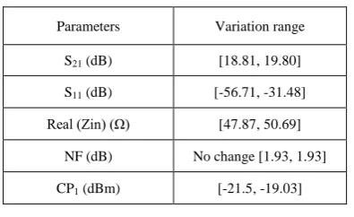
TABLE V. IMPACT OF THE OUTPUT MATCH CENTER FREQUENCY
CONTROL ON THE OTHER PARAMETERS OF THE LNA
AT 2.45GHZ
Parameters Variation range
S21 (dB) [18.81, 19.80]
S11 (dB) [-56.71, -31.48]
Real (Zin) (Ω) [47.87, 50.69]
NF (dB) No change [1.93, 1.93]
CP1 (dBm) [-21.5, -19.03]
IV. CONCLUSION AND FUTURE WORKS
This paper presented two techniques to control the input match and the output match of an inductively degenerated LNA. The simulation results show a control of the input match S11 between -33.12dB and -56.23dB. The input
match center frequency can be controlled between 2.361GHz and 2.603GHz. The control of the output match S22 can be achieved between -17.98dB and -53.65dB. The
center frequency of the output match can be controlled between 2.336GHz and 2.540GHz. We also demonstrated that the controls of these performances are made in an independent way. Besides, these controls have no significant effects on the other LNA parameters at 2.45GHz. Therefore, the methodology of the control shows the advantage of this proposed controllable circuit. These techniques are validated theoretically and through simulation using ideal tuning elements. As future works, we propose the implementation of these control elements. However, the implemented control elements contain parasitic elements that might affect the LNA performances. For this reason, we will use these techniques to compensate the LNA parameters shifts caused by these parasitic elements.
REFERENCES
[1] H. Donghoon, S. S. Akbay, S. Bhattacharya, A. Chatterjee, and W. R. Eisenstadt, “On-chip self-calibration of RF circuits using specification-driven built-in self test (S-BIST),” in Proc. 11th IEEE International Symposium on On-Line Testing, 6-8 July 2005, pp. 106-111.
[2] H. Donghoon, “Built-in self test and calibration of RF systems for parametric failures,” Ph.D. Dissertation, The Academic Faculty, Georgia Institute of Technology, May 2007.
[3] K. Jayaraman, Q. Khan, B. Chi, W. Beattie, Z. Wang, and P. Chiang, “A self-healing 2.4GHz LNA with on-chip S11/S21 measurement/calibration for in-situ PVT compensation,” in Proc. IEEERadio Frequency Integrated Circuits Symposium, May 2010, pp. 311-314.
[4] Y. Cui, B. Chi, M. Liu, Y. Zhang, Y. Li, P. Chiang, and Z. Wang, “Process variation compensation of a 2.4GHz LNA in 0.18um CMOS using digitally switchable capacitance,” in Proc.IEEE International Symposium on Circuits and Systems, May 2007, pp. 2562-2565.
[5] N. Ahsan, J. Dabrowski, and A. Ouacha, “A self-tuning Technique for optimization of dual band LNA,” in Proc. European Conference on Wireless Technology, October 2008, pp. 178–181. [6] D. K. Shaeffer and T. H. Lee, “A 1.5-V, 1.5-GHz CMOS low noise amplifier,” IEEE J. Solid-State Circuits, vol. 32, no. 5, pp. 745–759, May 1997.
[7] C. Garuda, X. Cui, P. C. Lin, S. J. Doo, P. Zhang, and M. Ismail, “A 3-5 GHz fully differential CMOS LNA with dual gain mode for wireless UWB applications,” in Proc. Midwest Symposium on Circuits and Systems, vol. 1, August 2005, pp. 790 – 793. [8] T. Das, A. Gopalan, C. Washburn, and P.R. Mukund, “Self
-calibration of input-match in RF front-end circuitry,” IEEE Trans. On Circuits and Systems II: Express Briefs,vol. 52, no. 12, pp. 821-825, December 2005.
[9] T. Das and P. R. Mukund, “Self calibration of gain and output match in LNAs,” in Proc. IEEE International Symposium on Circuits and Systems, September 2006, pp. 4983-4986.