Simulation of Nine Level Cascaded H-bridge Multilevel
DC-Link Inverter
N. Booma, Nagisetty Sridhar
Abstract–This paper presents simulation of the nine level cascaded H-bridge multilevel inverter based on a multilevel DC link (MLDCL) and a bridge inverter to reduce the number of switches. An MLDCL can be a diode-clamped phase leg, a flying-capacitor phase leg, or cascaded half-bridge cells with each cell having its own DC source. Compared to diode clamped & flying capacitor type MLDCL inverters cascaded H-bridge multilevel inverter requires least no of components to achieve same no of voltage levels. Optimized circuit layout is possible because each level have same structure and there is no extra clamping diodes or capacitors. Soft switching techniques can also be used to reduce switching losses and device stresses. The MLDCL provides a DC voltage with the shape of a staircase approximating the rectified shape of a commanded sinusoidal wave to the bridge inverter, which in turn alternates the polarity to produce an AC voltage. Compared with the existing type of cascaded H-bridge multilevel inverter, the MLDCL inverters can significantly reduce the switch count as well as the number of gate drivers as the number of voltage levels increases. For a given number of voltage levels, the required number of active switches is 2 (m-1) for the existing multilevel inverters, but it is m+3 for the MLDCL inverters. This paper aims to present analysis and simulation of cascaded H bridge multilevel dc link inverter. Matlab simulation has been done and simulation results of the cascaded H-bridge MLDCL inverter supplying induction motor load is discussed and it is proved that proposed inverter output has less THD compared to flying capacitor and diode clamped multilevel inverter.
Keywords — Cascaded half bridge, multilevel dc link, multilevel inverter, reduced component count, switching sequences.
I. INTRODUCTION
The voltage source inverters produce an output voltage or current with levels either 0 or ±Vdc. They are known as the two-level inverter. To produce a quality output voltage or a current wave form with less amount of ripple content, they require high switching frequency. In high- power and high-voltage applications these two level inverters, however, have some limitations in operating at high frequency mainly due to switching losses and constraints of device ratings [1]. These limitations can be overcome using multilevel inverters. The multilevel inverters have drawn tremendous interest in power industry. It may be easier to produce a high-power, high-voltage inverter with multi level structure because of the way in which the voltage stresses are controlled in the structure[3].
The unique structure of multilevel voltage source inverters allows them to reach high voltages with low harmonics without use of transformers or series connected synchronized-switching devices. As the number of voltage levels increases, the harmonic content of the output voltage
wave form decreases significantly. There are 3 types of multilevel inverters named as diode clamped multilevel inverter, flying capacitor multilevel inverter and cascaded multilevel inverter. These three types of multilevel inverters requires more no of components such as switches, clamping diodes and capacitors[10]. As the number of voltage levels m grows the number of active switches increases according to 2×(m-1) for the cascaded H-bridge multilevel inverters.
This paper presents a nine level cascaded H-bridge multilevel inverter based on an MLDCL and a bridge inverter. Compared with the existing cascaded multilevel inverters, the cascaded MLDCL inverters can significantly reduce the switch count as well as the number of gate drivers as the number of voltage levels increases. For a given number of voltage levels m, the cascaded MLDCL inverter requires m+3active switches, roughly half the number of switches Simulation results are included to verify the operating principle of the proposed MLDCL inverters.
II. C
ASCADEDH-B
RIDGEMLDCL I
NVERTERT
OPOLOGYFigure.1 shows a block diagram of the presented cascaded H-bridge MLDCL inverter topology, which consists of a multilevel DC source to produce DC-link bus voltage Vbus and a single-phase full-bridge (SPFB) inverter consists of four switches S1-S4 to alternate polarity of DC-link bus voltage to produce an AC voltage. The DC source is formed by connecting a number of half-bridge cells in series with each cell having a voltage source controlled by two switches Sak and Sbk. The two switches and operate in a toggle fashion. The cell source is bypassed with Sakon and Sbkoff, or adds to the dc-link voltage by reversing the switches. Figure.2 shows a circuit diagram of the presented cascaded H-bridge MLDCL inverter topology.
Fig.2. Circuit diagram of Cascaded H-bridge MLDCL inverter
The circuit diagram of the cascaded H-bridge multilevel DC-link inverter topology shown in Figure 2 consists of multilevel DC-link voltage source and single phase full bridge inverter.
A. Multilevel DC-link voltage source
Multilevel DC-link voltage source is formed by connecting a number of half-bridge cells in series with each cell having a voltage source controlled by two MOSFET switches as shown in the Figure 3. The two MOSFET switches will operate in a toggle fashion. Low on resistance and fast switching capability, low voltage MOSFETS are utilized in each cell source to reduce the inverter cost or to provide a high bandwidth sinusoidal output voltage. The MOSFET switches are triggered by proper switching signals to produce multi level DC-link bus voltage which is indicated by Vbusin the circuit diagram.
Fig.3. Multilevel DC-link voltage source
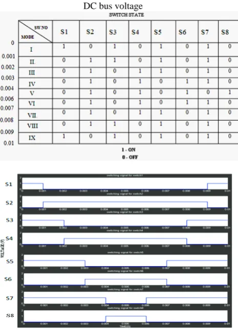
Various modes of switching sequence is given in the table 1 to produce DC bus voltage Vbuswith the shape of stair case with (n=4) steps, where n is the number of cell sources that is given to the SPFB inverter.
Based on the various modes given in table 1 switching signals are generated for the switches in the half bridge cells. The switching pulses are shown in Figure 4.
Table 1: Various modes of switching sequence to produce DC bus voltage
Fig.4. Switching pulses for switches in four H-bridge cells By giving the switching pulses shown in figure 4 to the switches in four H-bridge cells the MLDCL voltage source produces DC bus voltage Vbuswith the shape of stair case with (n=4) steps that approximates the rectified waveform of the commanded sinusoidal voltage, where n is the number of cell sources that is given to the SPFB inverter.The desired DC bus voltage Vbusis shown in the Figure 5.The switches in four cells will operate at twice of the fundamental frequency of the output voltage.
Fig.5. Desired DC bus voltage Vbus of cascaded H-bridge MLDCLI
B. Single phase full bridge inverter
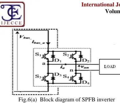
Fig.6(a) Block diagram of SPFB inverter The switches S1-S4 always work in pairs such that S1&S4 triggered for positive half cycle and S2&S3 will trigger with some delay to produce negative half cycle by operating the switches at the fundamental frequency of the output voltage. The switching sequence for producing multilevel AC output voltage is shown in Figure 6(a).
Fig.6(b) Switching signals of SPFB inverter C. Principle of operation of nine level cascaded H-bridge MLDCL inverter
The principle of operation of nine level cascaded multilevel DC-link inverter is explained by explaining the operating principles of multilevel DC link voltage source and single phase full bridge inverter. To produce nine level AC output voltage Vanthe multilevel DC-link source is formed by connecting four H-bridge cells in series with each cell having a separate voltage source controlled by two switches Sakand Sbkwhich will operate in a toggle fashion. The cell source is bypassed with Sakon and Sbkoff, or adds to the DC link bus voltage by reversing the switches. The DC bus voltage Vbusis fed to the SPFB inverter.
The switching signals shown in Figure 6(b) are given to the SPFB inverter in turn to alternate the voltage polarity of the DC bus voltage Vbusfor producing an AC output voltage Van of a stair case shape with (2n+1)=9 levels, whose voltages are -(V1+V2+...+ Vn) , -(V1+V2+...Vn-1)...,-V2, -V1 ,0, V1, V2,...(V1+V2+....Vn-1), (V1+V2+....Vn). Where V1, V2...Vn are voltages of cell sources. The desired AC output voltage Van of cascaded H-bridge is shown in the Figure 6(c).
Fig.6(c) Desired AC output voltage Van of cascaded H-bridge MLDCLI
III. S
IMULATIONR
ESULTSA detailed circuit simulation was conducted to verify the operating principles of the proposed MLDCL inverters. A. Nine level cascaded H-Bridge MLDCL Inverter with R load
A single-phase 9-level cascaded H-bridge MLDCL inverter was first studied for powering a resistive load, as shown in Figure 7. The load resistance is 30Ω and the voltage of each DC source is set at 30 V for an output frequency of 50 Hz.
The DC bus voltage Vbus, AC output voltage of the inverter Vanand AC output current ianare shown in Figures 7(a), 7(b) and 7(c) respectively. These waveforms confirm the principle of operation of 9-level cascaded H-bridge MLDCL inverter described in section II-C.
Fig.7. Simulation circuit of nine level cascaded H-Bridge MLDCL Inverter with resistive load
Fig.7 (b) Simulated AC output voltage waveform of nine level cascaded H-Bridge MLDCL Inverter with resistive
load
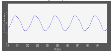
Fig.7 (c) Simulated AC output current waveform of nine level cascaded H-Bridge MLDCL Inverter with resistive
load
B. Nine level cascaded H-Bridge MLDCL Inverter with RL load
A single-phase 9-level cascaded H-bridge MLDCL inverter was studied for powering an inductive resistor load, as shown in Figure 8. The load resistance and inductance are 30Ω and 90 mH and 150 mH. The voltage of each DC source is set at 25 V for an output frequency of 50Hz.
The simulated DC bus voltage Vbus,AC output voltage of the inverter Vanand AC output current ianare shown in Figures 8(a), 8(b) and 8(c) respectively. These waveforms confirm the principle of operation of 9-level cascaded H-bridge MLDCL inverter described in section II-C with an inductive resistor load.
Fig.8. Simulation circuit of nine level cascaded H-Bridge MLDCL Inverter with inductive resistor load
Fig.8 (a) Simulated DC bus voltage waveform of nine level cascaded H-Bridge MLDCL Inverter with inductive resistor
Fig. 8 (b) Simulated AC output voltage waveform of nine level cascaded H-Bridge MLDCL Inverter with inductive
resistor load
Fig.8(c) Simulated AC output current waveform of nine level cascaded H-Bridge MLDCL Inverter with inductive
resistor load
The output voltage and current are in phase with each other for resistive load but there exists a phase lag between output voltage and current for an inductive resistor load due to presence of inductance in the load. The phase lag increases with the increase in inductance value. The simulated AC output current waveform with increased load inductance is shown in Figure 8(d).
Fig.8(d) Simulated AC output current waveform of nine level cascaded H-Bridge MLDCL Inverter with inductive
resistor load with increased load inductance. The line spectrum for the output current waveform is taken to determine the Total Harmonic Distortion present in the waveform. The Figure 9 shows the Total Harmonic Distortion is 7.24% for the output current of nine level cascaded H-Bridge MLDCL Inverter with RL load with increased load inductance.
Fig.9. FFT analysis of output current waveform of nine level cascaded H-Bridge MLDCL Inverter with inductive resistor
C. Nine level cascaded H-Bridge MLDCL Inverter with induction motor load
A single-phase 9-level cascaded H-bridge MLDCL inverter was studied for powering an induction motor load, as shown in Figure 10. The rating of the motor are power 1HP, voltage 230V. Main winding resistance and inductance are 2.02Ω and 0.0074 H and auxiliary winding resistance and inductance are7.14 Ω and 0.0085 H. The voltage of each DC source is set at 80 V to get 220 V rms voltage required for motor to run for an output frequency of 50 Hz.
The simulated AC output voltage of the inverter Vanand AC output current ianare shown in Figures 10(a)and 10(b) respectively. These waveforms confirm the principle of operation of 9-level cascaded H-bridge MLDCL inverter described in section II-C with an induction motor load.
Fig.10. Simulation circuit of nine level cascaded H-Bridge MLDCL Inverter with induction motor load
Fig.10. (b) Simulated AC output voltage waveform of nine level cascaded H-Bridge MLDCL Inverter with induction
motor load
Fig.10. (c) Simulated AC output current waveform of nine level cascaded H-Bridge MLDCL Inverter with induction
motor load.
The line spectrum for the output current waveform is taken to determine the Total Harmonic Distortion present in the waveform. The Figure 11 shows the Total Harmonic Distortion is 10.77% for the output current of nine level cascaded H-Bridge MLDCL Inverter with induction motor
Fig.11. FFT analysis of output current waveform of nine level cascaded H-Bridge MLDCL Inverter with induction
motor load
D. Comparison of the nine level cascade MLDCL Inverter and the existing MLI
From the previous discussions, it is demonstrated that the MLDCL inverters can significantly reduce the component count. Fig. 12 plots a chart for comparison of the required number of switches between the proposed MLDCL inverter and the cascaded H-bridge counterpart. As the number of voltage levels m grows, the number of active switches required is 2*(m-1) =16 for existing cascaded multilevel inverter and m+3 =12 switches are required for cascaded H-bridge MLDCL inverter[8]
Fig.12. Comparison of required number of switches.
IV. C
ONCLUSIONThe presented nine level cascaded H-bridge MLDCL inverters can eliminate roughly half the number of switches, their gate drivers compared with the existing cascaded MLI counterparts. Despite a higher total VA rating of the switches, the cascaded MLDCL inverters are cost less due to the savings from the eliminated gate drivers and from fewer assembly steps because of the substantially reduced number of components, which also leads to a smaller size and volume.
R
EFERENCES[1] Choi N.S, cho J.G,and cho G.H.,’a general circuit topology of multileve inverter’in.conf.rec.1991IEEE PESC,PP.96-103 . [2] Peng F.Z., Lai J. S., McKeever J.W., and VanCoevering J., ‘A
multilevel voltage-source converter system with balanced DC
voltages,’ in Conf.Rec. 1995 IEEE PESC, vol. 2, pp. 1144–1150 [3] Marchesoni M and Mazzucchelli M., ‘Multilevel converters for
high power AC drives: a review,’ in Proc. IEEE ISIE’93,
Budapest, Hungary,1993, pp. 38–43
[4] Ozpineci B., Tolbert L. M, Su G. J, Du Z, and Miller C. W.,
‘Optimum fuel cell utilization with multilevel converters,’in
Proc. 2004IEEE APEC’04, vol. 3, 2004, pp. 1572–1578 [5] Su G.J and Adams D. J., ‘Multilevel DC link inverter for
brushless permanent magnet motors with very low inductance,’
in Conf. Rec. 2001 IEEE-IAS Annu. Meeting, vol. 2, pp. 829–834.
[6] Takahashi.I, Iwaya.K ‘High efficiency, low harmonic distortion
switching type power amplifier using multilevel inverter,’ in
Proc. Power Conversion Conf.,vol. 2, Osaka, Japan, 2002, pp. 2–5.
[7] Gui-Jia Su’Multilevel DC link inverter’Industry
applications,IEEE Transactions on Volume: 41 , Issue: 3 Digital Object Identifier:10.1109/TIA.2005.847306.Publication Year: 2005 ,pp.848–854.
[8] Jianye Rao; Yongdong Li”Sensor-less Drive of Induction Motor Based on A New Hybrid Cascaded Multilevel Inverter”Applied Power Electronics Conference and Exposition, 2009. APEC 2009. Twenty-Fourth Annual IEEE , 2009 , Page(s): 1819 - 1823 [9] Fang Zheng Peng”A generalized multilevel inverter topology with self voltage balancing”….Industry Applications, IEEE Transactions on Volume: 37 , Issue: 2 ,2001 , Page(s): 611 - 618 [10] Panagis, P.; Stergiopoulos, F.; Marabeas, P.; Manias,
S,”Comparison of state of the art multilevel inverters”,Power Electronics Specialists Conference, 2008. PESC 2008. IEEE ,2008 , Page(s): 4296 - 4301
[11] Khoucha, F.; Lagoun, S.M.; Marouani, K.; Kheloui, A.; El Hachemi Benbouzid, M., Hybrid Cascaded H-Bridge Multilevel-Inverter Induction-Motor-Drive Direct Torque Control for Automotive Applications”,Industrial Electronics, IEEE Transactions on Volume: 57 , Issue: 3 ,2010 , Page(s): 892 -899
[12] Yi-Hung Liao; Ching-Ming Lai,” Newly-constructed single-phase multistring multilevel inverter for fuel-cell microgrid”,Power Electronics and ECCE Asia (ICPE & ECCE), 2011 IEEE 8th International Conference , 2011 , Page(s): 1440 -1444
A
UTHOR’
SP
ROFILEN. Booma
is an Assistant professor in Electrical and Electronics Engineering Department, Jerusalem College of Engineering, Chennai, India. She received her degree in Electrical & Electronics Engineering from, Madras University, Chennai, India in 2000, M.E. degree in Power Systems Engineering from College of Engineering, Guindy, Chennai, India in 2007. She has 11 years of teaching experience. She has published over 4 technical papers in national and international conferences proceedings. She is life member of Indian Society for Technical Education. Her research interests include Resonant converters, Intelligent controllers, FACTS, power quality.
Mr. Nagisetty Sridhar