Chemistry Publications
Chemistry
2007
Scanning tunneling microscopy and density
functional theory study of initial bilayer growth of
Ag films on NiAl(110)
Barış Ünal
Iowa State UniversityFeili Qin
Iowa State University, [email protected]
Yong Han
Iowa State University, [email protected]
Da-Jiang Liu
Iowa State UniversityDapeng Jing
Iowa State UniversitySee next page for additional authors
Follow this and additional works at:
http://lib.dr.iastate.edu/chem_pubs
Part of the
Materials Science and Engineering Commons
,
Mathematics Commons
, and the
Physical Chemistry Commons
The complete bibliographic information for this item can be found at
http://lib.dr.iastate.edu/
chem_pubs/34
. For information on how to cite this item, please visit
http://lib.dr.iastate.edu/
howtocite.html
.
This Article is brought to you for free and open access by the Chemistry at Iowa State University Digital Repository. It has been accepted for inclusion in Chemistry Publications by an authorized administrator of Iowa State University Digital Repository. For more information, please contact
initial bilayer growth of Ag films on NiAl(110)
Abstract
Scanning tunneling microscopy (STM) studies of the deposition of Ag on bcc NiAl(110) in the temperature
range from 200 to 300 K reveal an initial bilayer growth mode. In this regime, which encompasses at least the
first two levels of bilayer islands, the film appears to have an fcc Ag(110)-like structure. Selection of this
structure reflects an almost perfect lateral match between the Ag(110) and NiAl(110) lattice constants.
Density functional theory (DFT) analysis of supported Ag films with an ideal fcc(110) structure on
NiAl(110) indicates that the bilayer growth mode is promoted by a quantum size effect. However, the system
does not exhibit perfect Ag(110) film growth. STM analysis reveals that the tops of Ag islands are decorated
by a ripple structure even in the initial levels of growth and also shows a deviation from Ag(110)-like bilayer
growth to Ag(111)-like monolayer growth for thick films. DFT analysis is also applied to provide some
insight into the observed deviations from perfect Ag(110) film structure.
Keywords
Institute of Physical Research and Technology, Ames Laboratory, Materials Science and Engineering,
Mathematics
Disciplines
Materials Science and Engineering | Mathematics | Physical Chemistry
Comments
This article is from
Physical Review B
76, no. 19 (2007): 195410, doi:
10.1103/PhysRevB.76.195410
.
Authors
Barış Ünal, Feili Qin, Yong Han, Da-Jiang Liu, Dapeng Jing, A. R. Layson, Cynthia J. Jenks, James W. Evans,
and Patricia A. Thiel
Scanning tunneling microscopy and density functional theory study of initial bilayer growth of
Ag films on NiAl(110)
Baris Unal,1,2Feili Qin,3,2Yong Han,3Da-Jiang Liu,2 Dapeng Jing,4,2A. R. Layson,5Cynthia J. Jenks,2J. W. Evans,6,2and P. A. Thiel4,1,2
1Departments of Materials Science and Engineering, Iowa State University, Ames, Iowa 50011, USA 2Ames Laboratory-USDOE, Iowa State University, Ames, Iowa 50011, USA
3Institute of Physical Research and Technology, Iowa State University, Ames, Iowa 50011, USA 4Department of Chemistry, Iowa State University, Ames, Iowa 50011, USA
5Department of Chemistry and Biochemistry, Denison University, Granville, Ohio 43023, USA 6Department of Mathematics, Iowa State University, Ames, Iowa 50011, USA
共Received 18 June 2007; revised manuscript received 17 September 2007; published 9 November 2007兲 Scanning tunneling microscopy共STM兲studies of the deposition of Ag on bcc NiAl共110兲in the temperature range from 200 to 300 K reveal an initial bilayer growth mode. In this regime, which encompasses at least the first two levels of bilayer islands, the film appears to have an fcc Ag共110兲-like structure. Selection of this structure reflects an almost perfect lateral match between the Ag共110兲and NiAl共110兲lattice constants. Density functional theory共DFT兲analysis of supported Ag films with an ideal fcc共110兲structure on NiAl共110兲indicates that the bilayer growth mode is promoted by a quantum size effect. However, the system does not exhibit perfect Ag共110兲 film growth. STM analysis reveals that the tops of Ag islands are decorated by a ripple structure even in the initial levels of growth and also shows a deviation from Ag共110兲-like bilayer growth to Ag共111兲-like monolayer growth for thick films. DFT analysis is also applied to provide some insight into the observed deviations from perfect Ag共110兲film structure.
DOI:10.1103/PhysRevB.76.195410 PACS number共s兲: 68.55.Jk, 68.55.Ac, 68.35.Md, 68.37.Ef
I. INTRODUCTION
There has been extensive experimental and theoretical analysis for both homoepitaxial and heteroepitaxial growth of thin metal films.1–3 The great majority of these studies
have used single-element single-crystal substrates. However, using instead intermetallics as substrates or “templates” for thin film growth provides significant additional possibilities for guiding film structure and morphology. This strategy could potentially lead to novel nanostructures with tailored properties for surface enhanced Raman spectroscopy, cataly-sis, magnetism, or other applications.
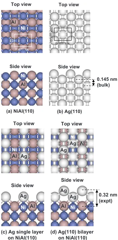
To explore such possibilities, in this paper, we examine the structure of Ag films grown on one such substrate, the binary alloy NiAl共110兲. This combination of materials is structurally intriguing because the bulk structures of the sub-strate and film are fundamentally different, NiAl being CsCl
共bcc-like, aNiAl= 0.289 nm兲 and Ag being fcc 共aAg = 0.408 nm兲. However, there is virtually perfect in-plane lat-tice matching between Ag共110兲and NiAl共110兲. This feature is illustrated in Figs.1共a兲and1共b兲. Consequently, this system provides an ideal candidate in which to study morphological evolution during heteroepitaxy in the absence of a lateral mismatch strain. In particular, it is of interest to determine whether Ag adopts the fcc共110兲structure atop this NiAl tem-plate.
The NiAl surface has attracted much attention in the past for several main reasons. First, NiAl is of technological im-portance in high-temperature applications such as turbines.4 Second, thin layers of alumina that are both well-ordered and conductive can be grown on this surface. These layers serve as tractable models for the alumina supports common in het-erogeneous catalysts.5 Third, the electronic structure of
NiAl共110兲includes a small depression in the density of states at the Fermi edge.6This feature has led to its selection as a substrate for growth of one-dimensional atomic wires both theoretically7and experimentally8–10共the latter being formed via atomic manipulation at low temperature兲, with focus on fundamental electronic and magnetic traits of the wires.
As a result of this widespread interest, the NiAl surface is reasonably well characterized. As shown in Fig. 1共a兲, the arrangement of atoms in the共110兲plane is anisotropic, con-sisting of rows of Ni and Al atoms in a 1:1 stoichiometry. In a previous structure determination using multiple scattering analysis of intensity-voltage variation of low-energy electron diffraction共LEED兲spots,11the共110兲surface was found to be
bulk terminated, except for two features. The first was a rum-pling of the top layer in which the Al atoms protrude above the Ni atoms by 0.02 nm. The second was a first interlayer expansion of a few percent共assuming that the Al atoms de-fine the topmost plane兲. The structure was confirmed by me-dium energy ion scattering12 and by x-ray scattering.13This
characterization was further supported by density functional theory 共DFT兲 calculations7,14 and reconfirmed in our own
analysis.
Numerous studies of Ag thin film growth on a variety of other substrates have been reported. From these, a few per-tinent generalizations can be drawn. First, Ag films do not alloy with other transition metal substrates at room ture. Alloying occurs in some systems, but only at tempera-tures of ⬃500 K or above.15–31 While Ag can insert into
surface planes of pure Al substrates,32 Ag is not known to
react with surfaces of alloys containing Al and earlier tran-sition metals such as Ni or Pd at room temperature.33,34
Pre-sumably, this is because the Al-Ni bond is much stronger than the Al-Ag or Ni-Ag bond, as reflected in the
thermody-PHYSICAL REVIEW B76, 195410共2007兲
namic data for the respective alloys.35–37 Thus, alloying is
not anticipated in the present work, wherein Ag is deposited at 200 and 300 K. Second, the low surface energy of Ag usually leads the first few layers to “wet” the substrate, al-though strain can trigger three-dimensional growth in higher layers共Stranski-Krastanov growth兲. An example of the latter is Ag on W共110兲.17,38Finally, clean films of Ag共and also Au兲 that are sufficiently thick—on the order of 10–50 layers or more—tend to exhibit an fcc共111兲orientation or be vicinal to the共111兲.33,39–42This tendency prevails on diverse substrates,
although details of the film morphology such as twinning and defect structure may depend on the interface, and some ex-ceptions can be found.
In Sec. II, we provide some background on our experi-mental procedures and on our supporting DFT calculations. In Sec. III, we present the main results of our study. First, we describe scanning tunneling microscopy共STM兲observations for multilayer growth of Ag films mediated by nucleation
and growth of islands within each level. In this paper, “layer” denotes an essentially flat, low-index atomic plane, whereas “level” corresponds to islands of a specific height, labeled according to sequence of appearance with increasing Ag cov-erage. We will argue that two Ag共110兲-like layers—i.e., a
共110兲bilayer—comprise each of the first two levels. We will propose that as the film thickens, a transition occurs and eventually single Ag共111兲-like layers—i.e., 共111兲 monolayers—comprise each level. DFT analyses of bench-mark ideal fcc Ag共110兲 film structures supported on a NiAl共110兲 substrate are then presented together with evi-dence that a quantum size effect promotes the initial bilayer growth. We also describe more subtle features of growth in-cluding rippling of the tops of Ag islands. Additional DFT analysis of other film structures is presented, which eluci-dates the rippling and which also provides insight into the deviation from bilayer growth for thicker films. Further dis-cussion is provided in Sec. IV. An appendix briefly describes the adsorption site of isolated Ag adatoms on NiAl共110兲, adatom diffusion, and the Ag-Ag interactions that lead to the observed island shapes.
II. DETAILS OF EXPERIMENTS AND CALCULATIONS A NiAl single crystal was grown using the Bridgman technique.43The samples were oriented and sectioned from
the ingot by electrical discharge machining. The NiAl sur-face was oriented to within ±0.25° of the共110兲 orientation and then polished using standard metallographic techniques. The polished sample was mounted on an Omicron heater and introduced into an ultrahigh-vacuum chamber equipped with Auger electron spectroscopy共AES兲, LEED, and STM. The base pressure of the chamber was 2⫻10−11Torr. The sample
was cleaned by repeated cycles of Ar+ sputtering 共20 min, 1.5 keV, andT= 300 K兲followed by annealing to 1200 K for 2 h, until the surface was judged clean by AES, LEED, and STM. The annealing temperature corresponds to about 2 / 3 of the melting point, 1915 K. STM images were processed usingWSXMsoftware.44
STM images reveal that these sample preparation proce-dures can produce a NiAl共110兲 surface with broad terraces
共up to 1m wide兲. In the data presented in this work, spe-cifically, the terraces were up to 110 nm wide for deposition of Ag at 300 K and up to 260 nm at 200 K. The terraces were separated by monatomic steps and step bunches. Line scans across these steps indicated a step height of 0.204± 0.006 nm, nearly equal to the value of 0.2014 nm expected from the bulk lattice constant of NiAl. We were thereby able to calibrate thez-piezo in the STM, a key re-quirement for subsequent characterization of vertical surface structure.
In thin film growth studies, Ag was evaporated from a commercial Omicron source. However, this source had a rather open design, and so we modified it with a cap contain-ing a 1.25 mm orifice. This made the arrangement more like a true Knudsen cell. The base pressure was below 10−10Torr
during deposition. Flux calibration of the source was achieved by measuring the coverage directly from the STM images at low coverage. The estimated flux value was 1.6 (a) NiAl(110)
Top view
Side view
Ni
Al
(b) Ag(110) Top view
Side view
0.145 nm (bulk) Ni
Al
0.409 nm
0.289
nm
0.408 nm
0.288
nm
Ni
Al
(c) Ag single layer on NiAl(110)
Top view
Side view
Ni Al
Top view
Side view
0.32 nm (expt)
(d) Ag(110) bilayer on NiAl(110) Ag
Ag
Ni
Ag Al Ag
Ni
Ag
[image:4.612.76.271.56.451.2]Al Ag
⫻10−3bilayer s−1 关where a bilayer is defined as two layers
of a perfect Ag共110兲 film兴 for the studies conducted at a surface temperature of 300 K and 3.3⫻10−3 bilayer s−1 for
those done at 200 K.
Some STM data are also reported for comparative studies of Ag deposition on Ag共110兲. These experiments were per-formed in a different chamber, with base pressure below 1 ⫻10−10Torr. The Ag共110兲sample was cleaned by repeated
cycles of Ar+ sputtering 共20 min, 0.5 keV, and T⬇300 K兲
followed by annealing at 700 K. The Ag was deposited at 220 K, and the flux was 4.5⫻10−2monolayer s−1.
For electronic structure calculations, we used DFT with the generalized gradient approximation proposed by Perdew et al.45 The single-particle Kohn-Sham equations46 were
solved using the plane-wave-based Viennaab initio simula-tion package共VASP兲.47The electron-ion interactions were
de-scribed by the projector augmented-wave approach.48 The
energy cutoff for the plane-wave basis was set to be the default value for freestanding or supported Ag共110兲 films. The converged magnitude of the forces on all relaxed atoms was always less than 0.1 eV/ nm. To prevent spurious inter-actions between adjacent replicas of the thin film system, we used a vacuum layer that was 1.5 nm thick in the direction perpendicular to the surface. The optimized lattice constants were 0.2896 nm for NiAl and 0.4166 nm for Ag, to be com-pared with the experimental values of 0.289 and 0.408 nm, respectively. These theoretical lattice constants were used in all subsequent calculations.
As background for analysis of supported Ag films on NiAl共110兲presented below, some brief remarks on the DFT predictions for the structure of the clean NiAl共110兲 surface follow. Our DFT calculations reproduced the experimental results reasonably well. For instance, the vertical separation between surface Ni and Al atoms is 0.017 nm from our DFT
关for a 21-layer NiAl共110兲slab兴, whereas it is 0.016 nm from x-ray scattering13 and 0.022 nm from LEED.11The first
in-terlayer spacing49is larger than the bulk value by 3.1% from
our DFT, compared with共3.8± 0.6兲% from x-ray scattering,13
4.6% from LEED,11 and 共5.0± 2.0兲% from medium energy
ion scattering.12Our calculations further showed that the
sur-face energy of clean NiAl共110兲 is 1.57 J / m2 for the fully
relaxed surface. This is, as might be expected, comparable to but lower than the value obtained from a previous DFT analysis of a fixed 共unrelaxed兲 substrate, 1.65 J / m2.50
Fur-thermore, it is higher than the surface energy of Ag共110兲, 1.24– 1.42 J / m2.51,52 Hence, surface energy differences
should drive Ag共110兲 films to grow layer by layer on NiAl共110兲, although this prediction is rather crude because it ignores the interfacial energy.
Finally, one might anticipate quantum size effects associ-ated with the finite thickness of the slab of NiAl共110兲 sub-strate used in calculations below for supported Ag films. In-deed, calculations for NiAl共110兲 slabs of various thickness did indicate some variations of the surface energy of thin Ag films. However, in this work, comparisons are made while holding the NiAl slab thickness constant, so this effect should not impact our analysis of relative energetics associ-ated with supported Ag films of various thicknesses.
III. EXPERIMENTAL AND THEORETICAL RESULTS FOR Ag FILMS ON NiAl(110)
A. Ag island step heights from scanning tunneling microscopy data
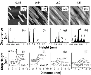
Figures2 and3 show STM images of Ag islands depos-ited on NiAl共110兲at 200 and 300 K, respectively, for various film thicknesses关the associated coverages being reported in units of Ag共110兲bilayers兴, together with representative infor-mation about step heights. From the STM images shown in the top row of each figure, it is clear that Ag forms two-dimensional islands. These islands are large and display
Distance (nm)
2 3
4
5 6 1
2
3 4
Height (nm)
0.15 0.54 2.0 4.5
0 1
2 0
1
(a) (b) (c) (d)
(e) (f) (g) (h)
(i) (j) (k) (l)
Level 1 Level 2 Level 4 Level 6
0.2 nm
Step
Height
(nm)
Occurrence
[image:5.612.50.361.52.310.2](au)
FIG. 2. STM data for Ag deposited on NiAl共110兲at 200 K as a function of cov-erage关measured in units of Ag共110兲 bilay-ers兴 shown above the STM images. The top row 关共a兲–共d兲兴 shows STM images of size of 100⫻100 nm2. The middle row 关共e兲–共h兲兴 shows pixel height histograms from a small areas of the surface corre-sponding to a single terrace of the sub-strate共and not necessarily from within the image in the top row兲. Peaks in the histo-grams are labeled with the island level. The average level is not exactly equal to the total coverage given the transition from bilayer to monolayer growth. The average level height from the histogram also de-pends strongly on the small area sampled, but not the step heights. The bottom row 关共i兲–共l兲兴shows representative step profiles for the levels indicated.
SCANNING TUNNELING MICROSCOPY AND DENSITY… PHYSICAL REVIEW B76, 195410共2007兲
highly anisotropic, rectangular shapes. Diffusion across ter-races is sufficiently rapid at 300 K that, for a terrace width of about 100 nm or less and for the deposition rate specified above, Ag islands grow outward from steps as long fingerlike protrusions. This behavior corresponds to step flow growth. Diffusion is slower at 200 K, so that islands nucleate and grow in the middle of terraces, as well as at step edges. See the Appendix for a brief discussion of terrace diffusion of individual Ag adatoms on NiAl共110兲, together with the strong anisotropy in adatom interactions which produces elongated islands and the adsorption site.
Histograms of the pixel heights in a smaller region of the surface共chosen within a single terrace of the substrate兲 are shown in the middle row of each figure. The separations between peaks 共which are labeled by the level of islands above the substrate兲correspond to the average island or step heightsdwithin the sampled region. The bottom rows show representative line profiles, from which representative values of the step heightsd can also be derived.共Profiles are taken from a variety of images at different locations on the surface, not just from the images shown.兲We analyze both line pro-files and histograms because propro-files show individual char-acteristics while histograms obscure individual peculiarities but provide objective average values.
As an aside, note that the average coverage quoted above the STM images does not correspond exactly to the average level of the film surface in the sampled region, where the latter can be extracted from the histograms. There are two reasons for this discrepancy. First, histograms are taken from small areas in which the local coverage can fluctuate signifi-cantly. Second, the density of Ag atoms depends on the level, as will be clear from the discussion below.
Figure 4 and Table I show average values of d, deter-mined from histograms, for islands in different levels. The
results are virtually identical when line profiles are used. It can be seen that there is no significant difference between step heights at 200 or 300 K. The step height is 0.32 nm for the first-level islands and is 0.29 nm for the second-level islands at both temperatures. These are about twice the value expected for a Ag共110兲 monolayer. As the island level in-creases 共moving higher up in the film兲, the step height de-creases and eventually levels off in the range of 0.21– 0.24 nm.
Electronic effects could influence measurements of step height. This possibility is strongest for the first-level islands, i.e., those directly atop the NiAl共110兲 substrate. Electronic effects can be revealed by changing the tunneling bias. A measurement of step height, for islands within the first level at 200 K, vs tunneling voltage is shown in the inset of Fig.4. The step height of 0.32 nm does not change strongly with bias voltage, and hence we conclude that 0.32 nm is a topo-graphic value共reflecting positions of ion cores兲. For higher-level islands, where growth resembles homoepitaxy, another electronic effect known as Smoluchowski smoothening could conceivably influence STM measurements if the islands were very small 共containing a few tens of atoms兲 and closely spaced共within a few tenths of a nanometer兲.53However, the
islands in our data are much too large and well separated for the Smoluchowski effect to be significant.
It is instructive to compare these Ag islands with the ones grown on the共110兲surface of bulk Ag. The latter are shown in Fig.5共a兲for deposition at 220 K. Like the Ag/ NiAl共110兲 islands, the Ag/ Ag共110兲 islands are flat and elongated. The histogram in Fig.5共c兲reveals that they have a step height of d= 0.15 nm. Furthermore, this is the step height of intrinsic surface terraces on Ag共110兲, which is also shown by Fig.
5共b兲. This value of d equals the bulk interplanar spacing, 0.145 nm, as shown in Fig.1共b兲.
0.20 0.6 1.8 4.5
2
3 4 1
Height (nm)
Level 1 Level 2 Level 4 Level 6
0
1
1
0 2
Distance (nm)
0.2 nm
4 5
6 3
(a) (b) (c) (d)
(e) (f) (g) (h)
(i) (j) (k) (l)
Occurrence
(au)
Step
[image:6.612.55.292.55.249.2]Height (nm)
FIG. 3. STM data for Ag deposited on NiAl共110兲at 300 K with increasing coverage关measured in units of Ag共110兲bilayers兴shown above the STM images. Top row关共a兲–共d兲兴 shows STM images of size of 100⫻100 nm2, middle row 关共e兲–共h兲兴 shows pixel height
histograms 共not necessarily from the image in the top row兲, and bottom row关共i兲–共l兲兴shows representative step profiles for the levels indicated. Peaks in the histograms are labeled with the island level.
0.10 0.15 0.20 0.25 0.30 0.35 0.40
0 2 4 6 8 10
Level
Step
H
eight
(nm)
Bias Voltage (V)
Ag(110) BL
Ag(111) ML Ag(100) ML
Ag(110) ML
0.31 0.33 0.35
-3 -2 -1 0 1 2 3
[image:6.612.318.556.58.226.2]The step height for Ag/ Ag共110兲is about half of the value for the first- and second-level islands of Ag/ NiAl共110兲. Whereas Ag islands on bulk Ag共110兲form single layers, we propose that Ag islands on NiAl共110兲are essentially Ag共110兲 bilayers, at least in the first two levels. The structure of a Ag bilayer of Ag共110兲 on NiAl共110兲 is illustrated in Fig. 1共d兲, and for completeness, the structure of a Ag共110兲monolayer is illustrated in Fig.1共c兲.
As noted above, the average island height decreases as island level increases. At the high-coverage limit, the heights of the Ag islands, 0.21– 0.24 nm, are bracketed by those ex-pected for Ag共111兲, 0.236 nm, or Ag共100兲, 0.204 nm, but are significantly larger than the step height of Ag共110兲, 0.145 nm. This indicates that bilayer growth does not con-tinue and that the atomic structure is not that of perfect Ag共110兲in the higher-level islands. Specifically, we propose that there is a transition from Ag共110兲-like bilayer growth to Ag共111兲-like monolayer growth. See also Sec. III D.
Finally, it should be noted that islands are sometimes ob-served within the second level, which does not fit the above description. These are illustrated in Fig.6. These anomalous islands are always 2 nm wide, and they range in length from about 5 to 30 nm. We find them only within the second
level. They are 0.09– 0.11 nm higher than the surrounding Ag surface constituting the top of first-level islands. Very occasionally, they merge with normal共higher and wider兲 bi-layer islands, as in Fig.6共d兲. In such a case, the width of the anomalous island is still 2 nm but its height is about 0.14 nm. These single-layer Ag islands may serve as precur-sors to the bilayer within the second level.
B. Benchmark density functional theory studies of structure and energetics for an ideal fcc Ag„110…/ NiAl„110…film:
Rational for initial bilayer growth
[image:7.612.339.533.63.228.2]We have performed extensive DFT calculations to assess the energetics of ideal Ag共110兲 films of various thicknesses on the NiAl共110兲substrate. In the surface free energy calcu-lations, we used a 共1⫻1兲 lateral unit cell, thus enforcing perfect lateral periodicity. We used 15⫻15⫻1 kmesh. Ag atoms in the first layer are located at the site between Ni
TABLE I. Heights of majority islands, in nm, in different levels. 共Examples of minority or “anomalous” islands are given in Fig.6
and described in the text.兲When two numbers are given for a single island level from STM data, the top entry is for deposition at 200 K and the bottom for 300 K. Data are provided for both height histo-gram and line profile analysis. For the line profiles, each entry is based on at least six profiles. In the DFT calculations, the first-level step heights are derived from the difference between the height of the ion cores of the top Ag atoms and the average height of the ion cores of the Ni and Al atoms in the top substrate layer.
Island level
STM histograms
STM line profiles
DFT of Ag共110兲bilayer films on NiAl共110兲
1 0.324± 0.010 0.334± 0.027 0.340
0.317± 0.027 0.324± 0.027
2 0.294± 0.008 0.292± 0.012 0.290
0.283± 0.005 0.282± 0.013
3 0.265± 0.006 0.263± 0.017 0.295
0.267± 0.002 0.254± 0.017
4 0.248± 0.008 0.248± 0.020 0.294
0.236± 0.007 0.242± 0.018
5 0.241± 0.015 0.237± 0.019 0.293
0.234± 0.009 0.237± 0.020
6 0.239± 0.014 0.234± 0.018 0.294
0.213± 0.012 0.233± 0.024
7 0.220± 0.010 0.225± 0.010 0.293
0.212± 0.011 0.225± 0.013
8 0.233± 0.014 0.224± 0.017 0.294
9 0.221± 0.009 0.215± 0.020 0.292
b
c
(a)
Height (nm)
Occurrence
(au)
0.146 nm
(c)
Height (nm)
Occurrence
(au)
[image:7.612.51.296.170.460.2](b)
0.146 nmFIG. 5.共a兲STM image of Ag deposition on Ag共110兲at 220 K. The Ag coverage is 0.3 monolayer, image size is 270⫻270 nm2,
scanning current is 0.3 nA, and scanning voltage is +1 V.共b兲 His-togram of pixel heights from areabin共a兲, encompassing two ter-race step edges.共c兲Histogram of pixel heights from areacin 共a兲, encompassing several islands on a single terrace.
(a)
(b)
(c)
(d)
(e)
FIG. 6. Examples of anomalous islands, indicated by arrows, following deposition of Ag at 200 K. These are atop first-level is-lands. In共a兲, one of these islands bridges two regions with “normal” step heights, illustrating its likely origin as a Ag共110兲monolayer. In each vertical pair, the top frame is the normal constant current im-age, and the bottom frame is the differentiated version. Each image is 50⫻50 nm2.
SCANNING TUNNELING MICROSCOPY AND DENSITY… PHYSICAL REVIEW B76, 195410共2007兲
[image:7.612.322.554.542.647.2]atoms of the substrate, the preferred binding site for isolated Ag adatoms on this surface.共See the Appendix.兲The struc-ture of the NiAl共110兲surface changes very little when these Ag共110兲films are added. This feature has been checked for films on a five-layer NiAl共110兲 slab with the bottom layer fixed. At the interface, there is still the rumpled NiAl struc-ture similar to that of the freestanding NiAl共110兲 surface mentioned in Sec. I. As the Ag共110兲film grows thicker共from 1 to 22 layers兲, the distance between the top-layer Al atom center and its nearest Ag atom center decreases from 0.203 nm and converges to 0.199 nm. The interlayer spacing between two Ag共110兲 layers is close to the calculated bulk value of 0.147 nm.
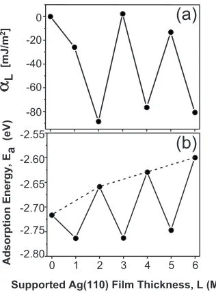
From an evaluation of the stability of ideal Ag共110兲films as a function of thickness, DFT provides a rationale for bi-layer growth. The quantity that best reflects the stability of the film as a function of its thickness in layersLis
␣L⬅␥t+␥b+␥i−␥t,0−␥b,0=
EL−E0−NLEc
A . 共1兲
Here,␥t,␥b, and␥iare the free energies of the top surface,
bottom surface, and interface, respectively. Generally speak-ing, all three energies are functions of film thickness.EL is
the total energy including the NiAl substrate,NLis the total
number of Ag atoms in the addedL layer Ag film,Ecis the
cohesive energy per atom of bulk fcc Ag, andAis the surface area. The subscript “0” corresponds to no Ag layer on the substrate. In our analysis, total energies共free energies at zero temperature兲 are calculated starting with a five-layer NiAl共110兲 slab as the substrate with the bottom layer fixed and adding layers of Ag共110兲. Figure7共a兲shows the
result-ing ␣L vs L for the first three bilayers. Oscillations with
bilayer period develop and persist to thicker films together with some beating 共not shown兲. It is clear that the most stable configurations共corresponding to minima in␣L兲occur
when films are two, four, and six layers thick.
The quantity ␣L describes the energetics of an extended
surface of a Ag共110兲 film supported on NiAl共110兲. One should also ask whether the adsorption or binding energy, Ea⬍0, of an individual,isolatedAg atom on perfect Ag共110兲
films of various thicknessesLwould oscillate similarly. This would be relevant to the initial stage of formation of each new bilayer. The relevant calculations are performed using a
共2⫻3兲 lateral unit cell with a 6⫻4⫻1 kmesh. In order to make the computation more efficient, the NiAl substrate is decreased to four layers in contrast to the above calculations, tests showing that this does not affect the basic results.
Figure7共b兲reveals that the adatom adsorption energy in-deed oscillates with a two-layer periodicity. These oscilla-tions persist for thicker films 共not shown兲. Comparing the values at the minima and maxima shows that it is signifi-cantly more favorable for an adatom to adsorb atop the first Ag layer共L= 1兲than atop the NiAl共110兲substrate 共L= 0兲. It is significantly more favorable to adsorb atop layerL= 3 than layerL= 2 and to absorb atop layerL= 5 than layerL= 4, etc. This underlies the tendency for bilayer growth. Furthermore, adsorption on higher even-numbered layers 共corresponding to L= 2,4,6兲 is progressively less favorable than on the NiAl共110兲substrate关the maxima in Fig.7共b兲connected by a dotted line move to higher values兴. This naturally leads each successive level of Ag to wet the surface, in accord with the crude surface energy arguments of Sec. II.
The oscillations in␣ andEa are promoted by a quantum
size effect共QSE兲. This effect originates from quantum con-finement of electrons in the vertical direction within the Ag film when the structural dimensions of a film become com-parable to the mean free path of electrons. More specifically, the stability pattern of a metal film depends on satisfying a matching condition involving the Fermi wavelength F and
the film interlayer spacingd.54If
F anddsatisfy the
condi-tion jd=iF/ 2, wherejandiare integers, then the film will
exhibit an oscillating stability with j-layer oscillation when j⫽i and no oscillation when j=i. For a Ag共110兲 film, d = 0.145 nm and F= 0.5228 nm. Then, when i= 1, j= 1.8,
which is close to the integer 2. This indicates that the Ag共110兲film has a primary stability oscillation with a period of two layers, in agreement with the DFT results for the first few layers.
The step heights calculated for the Ag共110兲 bilayers are shown in TableI. At the fourth bilayer, the step height has reached the asymptotic limit for thick films, 0.294 nm. For the first two levels, theory agrees well with experiment, sup-porting the interpretation that they are epitaxial Ag共110兲 bi-layers. At and especially beyond the third level, however, there develops a significant difference between calculation and experiment. This suggests that there is a transition from the QSE-stabilized structure to a different one at higher lev-els. See Sec. III A.
C. Ripples on the upper surface of the Ag(110) film Rather than displaying the “ideal” Ag共110兲structure in the first two levels, the upper surface of the Ag islands exhibits a
(b)
0 1 2 3 4 5 6
Supported Ag(110) Film Thickness, L (ML)
Adsorption
Energy,
Ea (eV) -2.55
-2.60
-2.65 -2.70 -2.75 -2.80
(a)
L[mJ/m
2]
0 -20 -40 -60
[image:8.612.90.248.58.272.2]-80
lateral structure consisting of linear ripples or stripes. Such features also occur in higher levels which do not have Ag共110兲 structure 共as surmised above based on their step heights兲. This ripple or stripe feature is shown in Fig.8. The stripes can be divided into two groups on the basis of their appearance and separation. The first types are imaged as de-pressions, i.e., dark lines, about 0.02 nm deep and either 0.8 or 1.2 nm apart. These depressions are illustrated in Figs.
8共a兲and 8共b兲. The second type appears as protrusions, i.e., bright lines, about 0.02– 0.05 nm high and separated by 3.3 nm 关Fig. 8共d兲兴. Between these protrusions, depressions are usually visible. Ripples separated by other distances, such as 1.8, 2.3, and 2.6 nm, can also be found, but they are uncommon. The ripples develop as a function of increasing film height or level. The depressions appear in the first level, but the 3.3 nm protrusions appear only in upper levels. Ripples are aligned across island steps, as is obvious in Figs.
8共d兲and8共e兲.
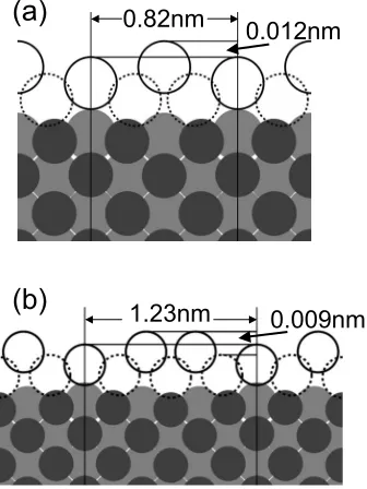
Our DFT analysis of ideal Ag共110兲film structures in Sec. III B used a 共1⫻1兲 lateral unit cell, thus enforcing lateral periodicity and excluding rippling. However, we have also performed a less restrictive DFT analysis which indicates that depressions in the first level could be due to a slight spontaneous rippling in the fcc共110兲 bilayer structure, i.e., rippling is not incompatible with and might reasonably be expected for perturbed Ag共110兲bilayer structures. These ad-ditional DFT calculations were performed using共n⫻1兲 su-percells, placing 2n Ag atoms 共to represent the first-level islands兲on top of a slab of six layers of NiAl共110兲substrate. The first five layers of the substrate were allowed to relax.
Forn= 2共with a period 0.82 nm兲, a rippled structure with an amplitude of 0.009 nm is found. This structure is energeti-cally more favorable than the unrippled one by 2 meV per unit cell. With n= 3 and therefore a period of 1.23 nm, a rippling consisting of two rows of high Ag separated by one row of lower Ag atoms is found. The amplitude is again
about 0.009 nm. The structure is favored by about 0.9 meV per unit cell over the flat structure. See Fig.9for side views for n= 2 and n= 3. With n= 4, aside from a period 0.82 nm rippled structure共trivially obtained from two of the above-mentioned n= 2 structures兲, another 共metastable兲 structure with 1.64 nm periodicity and even larger ripples can be found. However, it is less favored than the flat structure. For then= 2 andn= 3 structures, the periods of the ripples are in good agreement with those observed experimentally, and the amplitude of the rippling agrees to within a factor of 2. One cannot give a simple unambiguous identification of the dominant driving force for rippling, but one might note that while the lateral mismatch between the substrate and Ag共110兲 film is small, there is significant strain inherent in the different crystal structures of the two materials共bcc-like vs fcc兲.
Of course, one should not expect DFT to reliably predict such small energy differences between the unrippled and rippled structures. However, the calculations do show that it is plausible for rippled structures to have slightly lower en-ergies. Note that the effect on determining film structure of this small energy difference per unit cell is cumulative: for Ag films with long islands or rows of atoms, the energy difference between an unrippled and a rippled structure per row is the energy difference per atom times the length of the row. Furthermore, since the topological difference between the flat and rippled structures is very small, one can argue that there is very little共if any兲energy barrier for the transi-tion between them, so the system will easily find the rippled structure if it is indeed more energetically favorable. The fact that both separations 共0.8 and 1.2 nm兲 are observed in ex-periment indicates that there is a competition between the
[image:9.612.354.522.61.285.2](a)
(b)
(c)
(d)
(e)
FIG. 8. Examples of ripples in the Ag islands at various levels. The top row shows images in the constant current mode, which makes depressions distinguishable from protrusions. The bottom row shows images that have been differentiated, which makes the ripples more identifiable. Each image is 23⫻23 nm2.共a兲First level, 300 K, depressions with period 1.2 nm.共b兲First level, 300 K, de-pressions with period 0.8 nm. 共c兲 First level, 200 K, depressions with both 0.8 and 1.2 nm periods. 共d兲 Third and fourth levels, 300 K, 3.3 nm protrusions, plus depressions. 共e兲 Fifth and sixth levels, 300 K, mixed periods with dislocations. The dislocations form a vertical column in the image. The white arrows point to two examples.
(b)
(a)
0.82nm
1.23nm
0.012nm
0.009nm
FIG. 9. DFT predictions for the rippled structure of a Ag共110兲 bilayer of periodicities共a兲n= 2 and共b兲n= 3. To make the rippling visible, all deviations 共of all species, in all directions兲 from the unrippled bilayer Ag共110兲atom positions are magnified by a factor of 10. Open circles are Ag, darkest circles are Ni, and light gray circles are Al.
SCANNING TUNNELING MICROSCOPY AND DENSITY… PHYSICAL REVIEW B76, 195410共2007兲
[image:9.612.59.291.61.166.2]two, which may be affected by factors such as defects or growth history.
Since we do not have a detailed model for the structure of the Ag film above the first two bilayers, it is more difficult to characterize the 3.3 nm protrusions that appear on higher terraces. The amplitude of these ripples seems to increase gradually from the second level to the fourth; in the fourth and higher levels, their amplitude is constant at about 0.05 nm. The progression with level height is illustrated in Fig.10, where one of the Ag islands crosses a step edge at the arrow. Different levels are labeled numerically. The 3.3 nm protrusions are clearly more pronounced on the fourth-level Ag islands than on the third-level island, and least of all on the second-level island. Hence, the develop-ment of the 3.3 nm protrusions seems to correlate with the decrease in step height共and transition from bilayer to mono-layer growth兲shown in Fig.4 and TableI. That is to say, in levels 2–4, the step height decreases and the protrusions de-velop in parallel. At and above level 4, both features are constant.
D. Other structures of the Ag film
We should emphasize that for initial Ag film growth on NiAl共110兲, our DFT calculations indicate that there is not a strong energetic driving force preferring the Ag共110兲 struc-ture over all other strucstruc-tures. Indeed, there are a variety of monolayer structures composed of local hexagonal, i.e., Ag共111兲-like, and square, i.e., Ag共100兲-like, motifs for which we find that DFT actually predicts a lower energy per atom than the Ag共110兲structure共although the energy difference is only ⬃0.02 eV/atom兲. However, these structures do not match the experimentally measured island or step heights. Assuming that these structures do actually have lower energy than Ag共110兲-like films 共which is unclear given the uncer-tainty in DFT predictions兲, one must conclude that their for-mation is kinetically hindered relative to that of Ag共110兲 films. In this regard, we have found that the lowest energy position for a single Ag atom adjacent to a complete row of Ag atoms on the substrate is at the bridge site between two Ni atoms in the Ag共110兲 position, rather than in a closer threefold hollow position compatible with alternative denser structures. Thus, it is plausible that nucleation and growth of the Ag共100兲structure are favored, and conversion to another structure is inhibited.
We have also performed additional DFT analysis to ex-plore specific aspects of the stability of Ag共110兲 bilayer is-lands. We describe two such analyses here.
共i兲We have analyzed the single bilayer Ag共110兲structure with even larger共n⫻1兲 lateral unit cells than described in Sec. III C. These calculations have revealed that forn艌4, it is energetically favorable for the bilayer structure to convert to a structure with a higher density of atoms in the first layer than in the second layer. However, transition to such a struc-ture from a perfect or slightly rippled共with lateral period of 0.82 or 1.23 nm兲 bilayer 共110兲 structure is generally acti-vated, perhaps providing a rationale for why these structures are not realized, according to our proposed model, for the initial stages of film growth.
共ii兲We have also performed a DFT analysis to explore the structure of Ag共110兲bilayer islands of finite width. Here, we found a tendency for atoms in the first layer in a narrow island to contract laterally. This contraction provides the driving force for the above-mentioned rippled structures and potentially for Ag共111兲-like domain walls between Ag共110兲 regions.
Next, we consider the structure of thick films. As indi-cated above, our STM studies for prolonged growth reveal that ultimately, thick Ag films on NiAl共110兲 appear to de-velop a Ag共111兲-like structure. For a 40-layer film grown at 300 K, we find that islands are more isotropic compared with the highly elongated islands observed for thin films. The is-land edges are also faceted, with facets frequently displaying the 120° angles expected for a Ag共111兲-like hexagonal struc-ture. These features are shown clearly in Fig.11.
Perhaps the most complicated aspect of growth is the transition from initial Ag共110兲bilayer growth to the ultimate Ag共111兲-like monolayer growth. If the initial growth did have an ideal Ag共110兲structure, then it would be more dif-ficult to rationalize the transition away from this structure given the lack of lateral mismatch in this system. However,
2
3
4
2
3
4
4
4
(a)
[image:10.612.89.257.58.397.2](b)
we have shown in Sec. III C that the film never has an ideal Ag共110兲structure, displaying rippling even in the lowest lev-els. This initial rippling feature and perhaps the effect of substrate defects共such as deviations from stoichiometric sur-face composition, buried dislocations, and steps兲 could all produce perturbations from the ideal Ag共110兲 structure that might grow with film thickness. This could naturally lead to a reduction with increasing film height of the barrier to the development of non-Ag共110兲structures, and thus ultimately lead to the formation of the Ag共111兲-like structure.
IV. SUMMARY AND DISCUSSION
The main outcome of the present investigation is the find-ing that Ag films grow in a Ag共110兲 bilayer mode on NiAl共110兲, at least in the first two levels. The tendency for bilayer growth of these films is promoted by a QSE. The QSE, in turn, reflects a barrier to electron propagation at both the Ag-vacuum and Ag-NiAl interfaces.
Formation of bilayer islands on the nanometer scale has been observed in some other metal on metal film growth systems in the initial submonolayer stages of deposition. These systems include Ag/ Fe共100兲,55,56 Co/ Cu共111兲,57,58
Au/ Ag共110兲,59 and Fe/ Cu
3Au共001兲.60 Several mechanisms
have been suggested to drive such bilayer growth including magnetostriction effects, a combination of strain and ex-change processes, and QSE. A surfactant can also force bi-layer growth.61Sometimes, there is a barrier to the formation
of bilayer islands which restricts their nucleation to steps, or near to steps, on the surface.56,58One could easily conclude
that a terrace nucleation barrier exists here as well if only data at 300 K were available, but the 200 K data prove that is not true, in the Ag/ NiAl共110兲system. Instead, preferential nucleation at steps at 300 K here is due to heteroepitaxial step flow, i.e., preferential Ag atom capture at existing steps due to rapid diffusion across terraces on the time scale of deposition.
Many other systems have been reported to exhibit QSEs.62,63Usually, the film is a low-melting metal or
semi-metal, the most common ones being Ag, Cu, Pb, and Bi. Substrates are semiconductors 共Si and GaAs兲 and higher-melting elemental metals共Ni, Fe, Co, and V兲. Additionally, quasicrystals 共a type of intermetallic兲 can support QSEs.64
Usually, these substrates have a gap or a pseudogap that serves to confine valence electrons within the film. In the
present case, the existence of a barrier at the Ag-NiAl inter-face can be rationalized similarly in terms of the small re-duction in the electron density of states at the Fermi edge in NiAl共110兲.6 Note also that in the electronic growth model,
the period of oscillation depends on the Fermi surface; the two-layer period observed here is a feature specific to the details of the Ag/ NiAl共110兲system.
Finally, we reiterate the particularly appealing feature of the Ag/ NiAl共110兲 system which both motivated and facili-tated this study: the almost perfect lateral match between the NiAl共110兲substrate and Ag共110兲 film. As noted above, this allows analysis of heteroepitaxial growth in the absence of a strong lateral mismatch strain. However, it also leads to the formation of an interface between substrate and film with a simple and natural structure amenable to detailed high-level theoretical analysis of the supported films共which is not pos-sible for some more complex metal-on-semiconductor or metal-on-quasicrystal systems兲.
ACKNOWLEDGMENTS
This work was supported primarily by NSF Grant No. CHE-0414378. D.-J.L. was supported by the Division of Chemical Sciences, Basic Energy Sciences, US Department of Energy共USDOE兲. The work was performed at the Ames Laboratory which is operated for the USDOE by Iowa State University under Contract No. DE-AC02-07CH11358.
APPENDIX: BINDING SITES AND DIFFUSION BARRIERS FOR ISOLATED Ag ADATOMS ON NiAl(110) We have performed a fairly comprehensive DFT evalua-tion of the potential energy surface for the adsorpevalua-tion or binding energy共as a function of lateral position兲 of an iso-lated Ag adatom on NiAl共110兲. This analysis shows that the most favorable adsorption site is at the bridge site between two nearest-neighbor Ni atoms, as shown in Fig. 1共c兲. In these calculations, the adsorption energy is defined as Ea
=Etot−Eslab, whereEtotis the total energy of the slab plus the adatom and Eslab is the total energy of the slab without the
adatom. In calculating Ea, we use a 2⫻3 supercell with 4
⫻4⫻1kmesh. The result isEa= −2.72 eV for this Ni-bridge
site. The next-most-favorable site is the quasithreefold site that lies slightly off center from the Al-bridge site, defined by a triangle of Al-Al-Ni, whereEa= −2.52 eV. The
determina-tion of the Ni bridge as the favored site for Ag adsorpdetermina-tion agrees with the experimental result of Walliset al., derived from atomically resolved STM.65 Our DFT analysis also
in-dicates that the barrier for diffusion of Ag between the Ni-bridge sites is about 0.27 eV关either in the direction parallel or perpendicular to the Ni rows shown in Fig.1共a兲兴.
It is not immediately clear why the Ni-bridge site should be favored over the Al-bridge site. For fcc共100兲surfaces of pure Al and Ni, our DFT calculations show that the adsorp-tion energies of Ag adatoms at fourfold hollow sites are es-sentially identical, i.e., −2.80 eV on Al vs −2.78 eV on Ni. For the共111兲 faces, Ag actually prefers Al, the binding en-ergy at threefold hollow sites being −2.32 eV on Al vs
[image:11.612.89.261.61.146.2](a) (b)
FIG. 11.关共a兲and共b兲兴STM images of a Ag film, about 40 layers thick, on NiAl共110兲at 200 K. Several sets of 120° angles are illus-trated with the white lines. The images have been differentiated to accentuate the step edges. Each image size is 100⫻100 nm2.
SCANNING TUNNELING MICROSCOPY AND DENSITY… PHYSICAL REVIEW B76, 195410共2007兲
−2.12 eV on Ni. These calculations use the true physical lattice constants for the Ni and Al surfaces. However, if we use a single bulk lattice constant 共the average of the two, 0.378 nm兲to make a comparison that is more relevant to the bimetallic alloy, then on the fcc共100兲faces, the binding pref-erence is reversed: the binding energy is 0.31 eV lower
共more negative兲on Ni than on Al. If this difference is pro-rated according to the number of metal atoms at the adsorp-tion site, then on NiAl共110兲, one expects Ag to prefer the Ni-bridge site by about 0.15 eV, close to the calculated value of 0.20 eV. We therefore suggest that the site preference is
very sensitive to the Ni-Ni共or Al-Al兲separation at the alloy surface.
Finally, we briefly remark on the extension of these DFT analyses to Ag adatom pair interactions. Not surprisingly, one finds a much stronger attractive interaction between Ag on neighboring Ni-bridge sites aligned with the Ni rows rather than orthogonal to these rows. This explains the ten-dency for islands to be strongly elongated in the direction of the Ni rows, analogous to the elongation of Ag islands on Ag共110兲in the direction of the rows of Ag in the top surface layer.
1J. W. Evans, P. A. Thiel, and M. C. Bartelt, Surf. Sci. Rep. 61, 1 共2006兲.
2H. Brune, Surf. Sci. Rep. 31, 121共1998兲.
3R. Q. Hwang and M. Bartelt, Chem. Rev.共Washington, D.C.兲 97,
1053共1997兲.
4V. K. Sikka, S. C. Devvi, S. Viswanathan, R. W. Swindeman, and
M. L. Santella, Intermetallics 8, 1329共2000兲.
5J. Libuda and H.-J. Freund, Surf. Sci. Rep. 57, 157共2005兲. 6S.-C. Lui, M. H. Kang, E. J. Mele, E. W. Plummer, and D. M.
Zehner, Phys. Rev. B 39, 13149共1989兲.
7J. Hong, Phys. Rev. B 73, 092413共2006兲.
8N. Nilius, T. M. Wallis, and W. Ho, Science 297, 1853共2002兲. 9N. Nilius, T. M. Wallis, M. Persson, and W. Ho, Phys. Rev. Lett.
90, 196103共2003兲.
10M. Persson, Phys. Rev. B 70, 205420共2004兲.
11H. L. Davis and J. R. Noonan, Phys. Rev. Lett. 54, 566共1985兲. 12S. M. Yalisove and W. R. Graham, Surf. Sci. 183, 556共1987兲. 13X. Torrelles, F. Wendler, O. Bikondoa, H. Isern, W. Moritz, and
G. R. Castro, Surf. Sci. 487, 97共2001兲.
14M. H. Kang and E. J. Mele, Phys. Rev. B 36, 7371共1987兲. 15T.-H. Kim, B.-Y. Choi, Y. J. Song, W. G. Park, S.-J. Kahng, and
Y. Kuk, Phys. Rev. B 67, 233401,共2003兲.
16H. Roder, R. Schuster, H. Brune, and K. Kern, Phys. Rev. Lett. 71, 2086共1993兲.
17C. Deisl, E. Bertel, M. Burgener, G. Meister, and A. Goldmann,
Phys. Rev. B 72155433共2005兲.
18D. B. Danko, M. Kuchowicz, R. Szukiewicz, and J.
Kolaczk-iewicz, Surf. Sci. 600, 2258共2006兲.
19T. Valia and M. Milun, Surf. Sci. 315, 81共1994兲.
20M. Pivetta, F. Patthey, and W.-D. Schneider, Surf. Sci. 532, 58 共2003兲.
21H. Noro, R. Persaud, and J. A. Venables, Surf. Sci. 357, 879 共1996兲.
22M. Parschau, D. Schlatterbeck, and K. Christmann, Surf. Sci. 376, 133共1997兲.
23D. Schlatterbeck, M. Parschau, and K. Christmann, Surf. Sci. 418, 240共1998兲.
24T. Ito, K. Umezawa, and S. Nakanishi, Appl. Surf. Sci. 130–132,
497共1998兲.
25S. Nakanishi, K. Umezawa, M. Yoshimura, and K. Ueda, Phys.
Rev. B 62, 13136共2000兲.
26R. Schuster, H. Roder, K. Bromann, H. Brune, and K. Kern, Phys.
Rev. B 54, 13476共1996兲.
27M. Batzill and B. E. Koel, Europhys. Lett. 64, 70共2003兲. 28G. A. Attard and D. A. King, Surf. Sci. 222360共1989兲. 29K. L. Man, Y. J. Feng, and M. S. Altman, Phys. Rev. B 74,
085420共2006兲.
30P. Pervan and M. Milun, Surf. Sci. 264, 135共1992兲.
31R. Fisher, T. Fauster, and W. Steinmann, Phys. Rev. B 4815496 共1993兲.
32V. Fournée, J. Ledieu, T. Cai, and P. A. Thiel, Phys. Rev. B 67,
155401共2003兲.
33V. Fournée, T. C. Cai, A. R. Ross, T. A. Lograsso, J. W. Evans,
and P. A. Thiel, Phys. Rev. B 67, 033406共2003兲.
34V. Fournee, A. R. Ross, T. A. Lograsso, J. W. Evans, and P. A.
Thiel, Surf. Sci. 537, 5共2003兲.
35S. S. Lim, P. L. Rossiter, and J. E. Tibballs, CALPHAD: Comput.
Coupling Phase Diagrams Thermochem. 19, 131共1995兲.
36L. Hammer, H. Graupner, V. Blum, K. Heinz, G. W. Ownby, and
D. M. Zehner, Surf. Sci. 412/413, 69共1998兲.
37Phase Equilibria, Crystallographic and Thermodynamic Data of Binary Alloys, edited by O. Madelung and B. Predel, Landolt-Börnstein, New Series, Group IV, Vol. 5A 共Springer, Berlin, 1991兲.
38E. Bauer, H. Poppa, G. Todd, and P. R. Davis, J. Appl. Phys. 48,
3773共1977兲.
39K. Reichelt and H. O. Lutz, J. Cryst. Growth 10, 103共1971兲. 40V. Y. Aristov, M. Bertolo, K. Jacobi, F. Maca, and M. Scheffler,
Phys. Rev. B 48, 5555共1993兲.
41G. Neuhold, L. Bartels, J. J. Paggel, and K. Horn, Surf. Sci. 376,
1共1997兲.
42K.-J. Chao, Z. Zhang, P. Ebert, and C. K. Shih, Phys. Rev. B 60,
4988共1999兲.
43Single crystals synthesisized at the Materials Preparation Center.
See www.mpc.ameslab.gov
44I. Horcas, R. Fernandez, J. M. Gomez-Rodriguez, J. Colchero, J.
Gomez-Herrero, and A. M. Baro, Rev. Sci. Instrum. 78, 013705 共2007兲.
45J. P. Perdew, K. Burke, and M. Ernzerhof, Phys. Rev. Lett. 77,
3865共1996兲.
46W. Kohn and L. J. Sham, Phys. Rev. 140, A1133共1965兲. 47G. Kresse and J. Hafner, Phys. Rev. B 47, 558共1993兲. 48G. Kresse and D. Joubert, Phys. Rev. B 59, 1758共1999兲. 49Note that the location of any layer is potentially complicated by
spacing is usually taken from experiment as the distance be-tween the second layer and the plane containing the topmost Al atoms. In DFT, we find a rumpling in the second layer of 0.003 nm, which would probably be undetectable by experiment and which has a very small effect on the interplanar spacing. In DFT, we take the first interplanar spacing as the separation be-tween adjacent planes of Al atoms.
50V. M. Kuznetsov, R. I. Kadyrov, and G. E. Rudenskii, J. Mater.
Sci. Technol. 14, 320共1998兲.
51L. Vitos, A. V. Ruban, H. L. Skriver, and J. Kollár, Surf. Sci. 411,
186共1998兲.
52M. J. Mehl and D. A. Papaconstantopoulos, Phys. Rev. B 54,
4519共1996兲.
53P. Bedrossian, B. Poelsema, G. Rosenfeld, L. C. Jorritsma, N. N.
Lipkin, and G. Comsa, Surf. Sci. 334, 1共1995兲.
54F. K. Schulte, Surf. Sci. 55, 427共1976兲.
55D.-A. Luh, T. Miller, J. J. Paggel, M. Y. Chou, and T.-C. Chiang,
Science 292, 1131共2001兲.
56K. L. Man, Z. Q. Qiu, and M. S. Altman, Phys. Rev. Lett. 93,
236104共2004兲.
57J. Ferrón, L. Gómez, J. J. de Miguel, and R. Miranda, Phys. Rev.
Lett. 93, 166107共2004兲.
58H. W. Chang, F. T. Yuan, Y. D. Yao, W. Y. Cheng, W. B. Su, C. S.
Cheng, C. W. Lee, and W. C. Cheng, J. Appl. Phys.100, 084304 共2006兲.
59P. Fenter and T. Gustafsson, Phys. Rev. B 43, 12195共1991兲. 60A. Verdini, L. Floreano, F. Bruno, D. Cvetko, A. Morgante, F.
Bisio, S. Terreni, and M. Canepa, Phys. Rev. B 65, 233403 共2002兲.
61C. Deisl, K. Swamy, E. Bertel, G. Meister, and A. Goldmann,
Surf. Sci. 600, 2900共2006兲.
62M. Milun, P. Pervan, and D. P. Woodruff, Rep. Prog. Phys. 65, 99 共2002兲.
63M. C. Tringides, M. Jalochowski, and E. Bauer, Phys. Today 60 共4兲, 50共2007兲.
64V. Fournée, H. R. Sharma, M. Shimoda, A. P. Tsai, B. Unal, A. R.
Ross, T. A. Lograsso, and P. A. Thiel, Phys. Rev. Lett. 95, 155504共2005兲.
65T. M. Wallis, N. Nilius, and W. Ho, J. Chem. Phys. 119, 2296 共2003兲.
SCANNING TUNNELING MICROSCOPY AND DENSITY… PHYSICAL REVIEW B76, 195410共2007兲