DESIGN MULTIPLE VALUE LOGIC FOR FULL ADDER
*,1
Mr. Dhanorkar
1
M.E Student of PRMCEAM
2EXTC Department
ARTICLE INFO ABSTRACT
Many developers have intended their models in binary and quaternary logic using 0.18µm CMOS technology. In Binary logic, circuit has limitations of increase interconnections giving rise to complexities and their by impact on size. Some authors concentrate
logic with MVL or quaternary logic to prevail over the limitation of size. Second is that for half and full adder (for addition/ arithmetic operations) the quaternary logic method required the conversion of quaternary log
Our aim is to intend and develop MVL or quaternary logic for fu
levels to binary logic. It will reduce the one additional step and improve the performance offer less chip size, saving more power. MVL or quaternary logic can be implemented in three different modes. From that mode, volt
dynamic power dissipation.
The design is targeted for the 0.18 μm CMOS technology. Design tool for simulation will be ADS [ADVANCED DESIGN SYSTEM] software. We will estimate
HAq / FAq without any need of conversion, and compare to existing binary circuits [HAb / FAb].
Copyright © 2015 Dhanorkar and Choudhary. This is an open access article distributed under the Creative Commons Att unrestricted use, distribution, and reproduction in any medium
INTRODUCTION
Multiple value logic are logical calculi in which there are more than two possible truth value. But Logical calculi are bivalent. There are only two possible values for any proposition true and false. Lukasiewiczs was first author who proposed two value and three value logic. i.e (True, false and unknown). Now four value logic i.e quaternary logic concept is new growing technology in VLSI. In this technology more than two value logic is implementing. MVL or quaternary logic means more than two truth value (0,1) logic i.e. n logic for n > 2. Here we implement four truth value logic i.e. (0,1,2,3). Several implementation methods have been proposed in the recent papers to realize the MVL circuits
Patel and Gurumurthy, 2010; Vasundara Patel and Gurumurthy; 2010; Radanovic and Syrzycki, 1996; Ricardo Cunha, 2007; Hirokatsu Shirahama and Takahiro Hanyu, 2008; Anindya Da1 et al., 2010). They can fundamentally be categorized as current-mode, voltage-mode and mixed circuits. current-mode circuits (Radanovic and Syrzycki, 1996; Ricardo Cunha, 2007; Hirokatsu Shirahama and Takahiro Hanyu, 2008; Anindya Da1 et al., 2010; Yasuda
Jean-Marc Philippe et al., 2005) have been popular and offer several benefits, the power consumption is high due to their inherent nature of constant current flow during the operation.
*Corresponding author: Dhanorkar, A. D.
M.E Student of PRMCEAM, Badnera-Amravati, (M.S) India.
ISSN: 0975-833X
Article History:
Received 19th January, 2015 Received in revised form 02nd February, 2015
Accepted 19th March, 2015
Published online 30th April,2015
Key words:
Increase data density,
Reduce dynamic power dissipation, Increase computational ability, Simple H/W,
Require less area/size.
RESEARCH ARTICLE
DESIGN MULTIPLE VALUE LOGIC FOR FULL ADDER
Mr. Dhanorkar, A. D. and
2Mr. Choudhary, P. S.
M.E Student of PRMCEAM, Badnera-Amravati, (M.S), India
artment of PRMCEAM, Badnera-Amravati, (M.S), India
ABSTRACT
Many developers have intended their models in binary and quaternary logic using 0.18µm CMOS technology. In Binary logic, circuit has limitations of increase interconnections giving rise to complexities and their by impact on size. Some authors concentrate
logic with MVL or quaternary logic to prevail over the limitation of size. Second is that for half and full adder (for addition/ arithmetic operations) the quaternary logic method required the conversion of quaternary logic level into binary level for implementation.
Our aim is to intend and develop MVL or quaternary logic for fu
levels to binary logic. It will reduce the one additional step and improve the performance offer less chip size, saving more power. MVL or quaternary logic can be implemented in three different modes. From that mode, voltage mode type model is beneficial to design and give high performance with less dynamic power dissipation.
The design is targeted for the 0.18 μm CMOS technology. Design tool for simulation will be ADS [ADVANCED DESIGN SYSTEM] software. We will estimate
HAq / FAq without any need of conversion, and compare to existing binary circuits [HAb / FAb].
is an open access article distributed under the Creative Commons Att and reproduction in any medium, provided the original work is properly cited.
Multiple value logic are logical calculi in which there are more than two possible truth value. But Logical calculi are bivalent. There are only two possible values for any proposition true and false. Lukasiewiczs was first author who posed two value and three value logic. i.e (True, false and unknown). Now four value logic i.e quaternary logic concept is new growing technology in VLSI. In this technology more than two value logic is implementing. MVL or quaternary than two truth value (0,1) logic i.e. n-value logic for n > 2. Here we implement four truth value logic i.e.
0,1,2,3). Several implementation methods have been proposed in the recent papers to realize the MVL circuits (Vasundara , 2010; Vasundara Patel and Gurumurthy; 2010; Radanovic and Syrzycki, 1996; Ricardo Cunha, 2007; Hirokatsu Shirahama and Takahiro Hanyu, 2008; . They can fundamentally be mode and mixed-mode Radanovic and Syrzycki, 1996; Ricardo Cunha, 2007; Hirokatsu Shirahama and Takahiro 2010; Yasuda et al., 1986; have been popular and offer power consumption is high due to their inherent nature of constant current flow during the operation.
Amravati, (M.S) India.
Alternatively, voltage-mode circuits consume a large majority of power only during the logic level switching. Hence, voltage-mode circuits do offer lesser power consumption which has been the key benefit of traditional CMOS binary logic circuits from the perspective of dynamic switching activity. Several approaches for quaternary circuit design have been proposed (Yasuda et al., 1986; Jean
2005; Wakui and Tanaka, 1989
Quaternary logic (radix-4-valued) is chosen as the base radix for the work reported here. Using a quaternary radix offers all the benefits of MVL such as reduced area due to signal routing reduction along with the important adv
easily interface with traditional binary logic circuits. For example a conventional 16 - bit bus (0 and 1) represents 65536 combinations. If we code the output with Quaternary logic (0, 1, 2 and 3), the width of the bus is reduced
result, we can reduce power and area requirement for the interconnection.
For the intend the various tools such as HSPICE, COSMOSCOPE, TANNER and ADS tools are available. ADS (Advance design system S/W) tool is popularly used and support the optimization of circuits. The organization of the paper is as follows: Section 2 explains discussion of previous research related to the proposed work. Implementation of quaternary half adder and full adder is shown in section 3. Conclusion part of the paper is given in section4.
International Journal of Current Research Vol. 7, Issue, 04, pp.15026-15030, April, 2015
INTERNATIONAL
DESIGN MULTIPLE VALUE LOGIC FOR FULL ADDER
Amravati, (M.S), India
(M.S), India
Many developers have intended their models in binary and quaternary logic using 0.18µm CMOS technology. In Binary logic, circuit has limitations of increase interconnections giving rise to complexities and their by impact on size. Some authors concentrated on put back in place of binary logic with MVL or quaternary logic to prevail over the limitation of size. Second is that for half and full adder (for addition/ arithmetic operations) the quaternary logic method required the conversion of
Our aim is to intend and develop MVL or quaternary logic for full adder without converting these levels to binary logic. It will reduce the one additional step and improve the performance offer less chip size, saving more power. MVL or quaternary logic can be implemented in three different modes. age mode type model is beneficial to design and give high performance with less
The design is targeted for the 0.18 μm CMOS technology. Design tool for simulation will be ADS area, power and delay of the design HAq / FAq without any need of conversion, and compare to existing binary circuits [HAb / FAb].
is an open access article distributed under the Creative Commons Attribution License, which permits
mode circuits consume a large majority of power only during the logic level switching. Hence,
mode circuits do offer lesser power consumption which has been the key benefit of traditional CMOS binary rom the perspective of dynamic switching activity. Several approaches for quaternary circuit design have 1986; Jean-Marc Philippe et al., 2005; Wakui and Tanaka, 1989), in voltage mode technique. valued) is chosen as the base radix for the work reported here. Using a quaternary radix offers all the benefits of MVL such as reduced area due to signal routing reduction along with the important advantage of being able to easily interface with traditional binary logic circuits. For bit bus (0 and 1) represents 65536 combinations. If we code the output with Quaternary logic (0, 1, 2 and 3), the width of the bus is reduced from 16 to 8. As a result, we can reduce power and area requirement for the
For the intend the various tools such as HSPICE, COSMOSCOPE, TANNER and ADS tools are available. ADS (Advance design system S/W) tool is popularly used and
ort the optimization of circuits. The organization of the paper is as follows: Section 2 explains discussion of previous research related to the proposed work. Implementation of quaternary half adder and full adder is shown in section 3.
f the paper is given in section4.
Literature review
Vasundara Patel , k s gurumurthy
“Design of high perfor-mance quatern-ary adders”, International Journal of Computer Theory and Engineering, Vol.2, No.6, December, 2010.
Theory Details
Author presented their work in the quaternary logic or MVL for half and full adder by using Q-B and B-Q conversion technique during implementation. The design implemented in 0.18µm CMOS technology and verified through HSPICE and COSMOSCOPE tool.
Our Finding
We find that in this technique during implementation, DLC circuit is used for conversion in intend model. By using conversion technique, intend model could not be achieved high performance (Vasundara Patel and Gurumurthy, 2010)
Vasundara Patel, k s gurumurthy.
“Arithmetic operations in multivalued logic. ”, International journal of VLSI, Vol.1, no.1,pp. 21-32, March 2010.
Theory Details
Author presented MVL for arithmetic operations like addition, subtraction and multiplications by using also Q-B and B-Q conversion in Galois field. They used 0.18µm cmos technology and HSPICE as tool for simulation and Karnaugh diagrams used for minimization of logic.
Our Finding
We find that this author implemented MVL or quaternary logic for all arithmetic operations. But they used module-n for conversion technique, so designed model could not be achieved high performance during operation (Vasundara Patel and Gurumurthy; 2010).
Bob Radanovic, Marek Syrzycki.
“Current-mode cmos adders using multiple-valued logic”, Canadian Conference on Electrical and Computer Engineering, pp.190-193, 1996.
Theory Details
Author presented the two design model for adder in current mode MVL. The first design of adder cell uses the radix-2 algorithm and 7 levels of current, fabricated in 0.8µm cmos technology with unit current step is 12µA. The second design is 4-digit decimal adder with standard algorithm and 10 current levels with 1.5µm cmos technology and 1µA unit current step.
Our Finding
We find that two major issues in the design of CMMVL are the numerical representation of numbers and the unit current
step per logic level. Because the numerical representation of number uses positive and negative current and unit current step per logic levels uses positive current. Due to inherent nature of current, the intend model is failed to achieve high performance (Radanovic and Syrzycki, 1996).
Ricardo Cunha, Henri Boudinov and Luigi Carro
“Quaternary look-up tables using voltage-mode CMOS logic design”, 37th ISMVL pp.56-56, 13-16 May, 2007.
Theory Details
Author presented a new logic functions, implemented using quaternary lookup tables. In this work, a quaternary multiplexer circuit is designed to implement any n-variable quaternary logic function based on its truth table. All circuits simulated with the Spice tool using TSMC 0.18 μm technology.
Our Finding
Quaternary look up table or mux in voltage mode cmos logic, design model gives high performance with less power dissipation and less no. of transistor as compared to current mode CM MVL. But the quaternary multiplexer circuit consists of Down Literal Circuits (Ricardo Cunha, 2007).
Hirokatsu Shirahama and Takahiro Hanyu
“Design of high-performance quaternary adders based on output-generator sharing”, 38th ISMVL, pp. 8-13. 2008.
Theory Details
Author proposed a design model of quaternary full adders based on output generator sharing in CM and VM mode. Arbitrary quaternary functions are performed by converting the quaternary inputs into binary and generating the desired quaternary outputs. The generating of desired quaternary outputs sharing with some processing elements like flip flop, comparators.
Our Finding
We find that this proposed model is achieved high performance in voltage mode. The delay and power dissipation of the proposed model in voltage-mode during implementation are reduced to 73 percent and 79 percent, respectively. But by using I/P conversion technique, interconnection complexity and area/ size increases (Hirokatsu Shirahama and Takahiro Hanyu, 2008).
Anindya Das1, Ifat Jahangir2 and Masud Hasan
“Design of quaternary serial and parallel adders”, 6th ICECE 2010, 18-20 December 2010, Dhaka, Bangladesh.
Theory Details
implemented the design of a logarithmic stage parallel adder which can compute the carries within log2(n) time delay for n qudits have limited number of fan-in.
Our Finding
We find that, they have utilized the associated algebra to design different kinds of expressions for full adder in quaternary logic system. They have proposed a design of logarithmic stage carry-tree adder which has time delay of log2(n) due to its tree structure (Anindya Da1 et al., 2010).
Y. Yasuda, Y. Tokuda, S. Zhaima, K. Pak, T. Nakamura A. Yoshida
“Realization of quatern-ary logic circuits by N-channel Mos devices”, IEEE Journal of Solid State Circuits, Vol.21, no.1, pp.162-168, 1986.
Theory Details
Author presented a new method, such as inverter, NAND, NOR, and delta literal circuits have been fabricated by conventional NMOS technology in quaternary logic.
These circuits are comprised of MOS transistors with three values of enhancement-mode threshold voltage and one depletion-mode threshold voltage.
Theory Details
We find that by implementing this method, the main advantage is the small number of MOST’s required, using simple layout patterns which allow direct comparison with circuit diagrams, and exact transfer characteristics (Yasuda
et al., 1986).
Jean-Marc Philippe, S´ebastien Pillement, Olivier Sentieys
“A low-power and high-speed Quaterna-Ry Interconn-Ection link using efficient converters”, ©2005 IEEE.
Theory Details
They introduce a new quaternary link including a binary to quaternary encoder and a quaternary-to-binary decoder in voltage mode multiple-valued logic (MVL). This link improves the transistor count compared to existing designs and it has no DC current path.
Our Finding
We find that, here again use of Q-B and B-Q conversion for designing the encoder and decoder. Whenever the conversion is used h/w complexity, area/size increases (Jean-Marc Philippe et al., 2005).
Kawahito, S. Kameyama, Higuchi, Yamada IEEE Member
“A 32 x 32-bit multipli-Er using multiple-valued MOS current- mode circuits”, IEEE Journal Of Solid-State Circuits, Vol. 23. No. 1, February 1988.
Theory Details
Author designed A 32x32-bit multiplier LSI with binary input and output has been designed using multiple-valued current-mode circuits and implemented in 2-µm CMOS technology. The multiplier, based on the radix-4 SD number system is realized by a regular array structure using a three-stage binary-tree scheme.
Our Finding
We find that, author presented a new design model MVL for multiplier. This model is LSI (large scale integrated) model with large h/w complexity. In this design model CM mode circuit failed to achieved high performance. Due to inherent nature of current (Wakui and Tanaka, 1989).
Vasundara patel K S. Dr K S Gurumurthy
“Multi-valued logic addition and multiplica-tion in galois field”, 2009 International Conference on Advances in Computing, Control, and Telecommunication Technologies.
Theory Details
Author presented a design model on the basis of MVL for Modulo-4 addition and multiplication. Logic design of each operation is achieved by reducing the terms using Karnaugh diagrams. Hspice simulation tool is used with 0.18µm cmos technology.
Our Finding
We find that here again author used a module -4 addition and multiplication. Module-4 operation is used for Q-B and B-Q conversion. Whenever conversion is used design model is failed to achieve high performance (Vasundara Patel and Gurumurthy, 2009).
Proposed Work
In this paper we will propose the quaternary half adder and full adder by using quaternary input and will obtained the quaternary output without using any converter. No need to convert the quaternary input into binary or binary to quaternary. From this method we can minimize the h/w implementation, power dissipation of circuit, require less number of transistor and we will achieve the high performance.
Implementation of quaternary / MVL for half adder
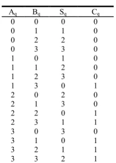
In quaternary logic, addition can be performed in many ways. Numbers in quaternary logic can be directly added or numbers in quaternary logic can be converted to binary logic and addition can be performed in binary logic. Binary results of addition can be displayed in quaternary logic after conversion. But we will perform the addition only by using quaternary logic only. In (Vasundara Patel and Gurumurthy, 2009) modulo-4 addition is introduced, implementation of carry without hardware. Figure 1 explains the block diagram of quaternary half adder and table. Aq and Bq are quaternary input numbers and Sq and Cq are the quaternary output numbers.
Fig.1. Block diagram of quaternary half adder Figure 2. Proposed quaternary full adder
Implementation of Quaternary full adder
Proposed full adder circuit is based on Quaternary adder. Block diagram of the full adder circuit is shown in figure 2. Aq and Bq are the two quaternary inputs to the full adder. Table 2 shows sum and carry for all possible combinations of inputs when carry input is zero. Table 3 shows sum and carry for all possible combinations of inputs when carry input is one. Aq, Bq and Cin q are quaternary input numbers and Sq and Cq are the quaternary output numbers.
Conclusion
In this paper we review the historical developments in this field, both in circuit realizations and in methods of handling multiple-valued design circuit. In the recent years MVL gaining the importance due to its inherent benefits like high speed , low area , and low dynamic power dissipation (VM), we found during analysis of MVL, it has great high message communication ability. In earlier work quaternary logic or (MVL) (Vasundara Patel and Gurumurthy, 2010; Vasundara Patel and Gurumurthy; 2010; Radanovic and Syrzycki, 1996; Ricardo Cunha, 2007; Hirokatsu Shirahama and Takahiro Hanyu, 2008; Anindya Da1 et al., 2010; Yasuda et al., 1986; Jean-Marc Philippe et al., 2005; Wakui and Tanaka, 1989; Vasundara Patel and Gurumurthy, 2009), arithmetic operations like addition, subtraction and multiplications presented which use Q-B conversion, B-Q conversion for implement the arithmetic operation. We proposed half adder and full adder in quaternary to quaternary without any conversion which then lead more optimization at farther level.
REFERENCES
Anindya Da1, Ifat Jahangir and Masud Hasan, 2010. “Design of quaternary serial and parallel adders”, ICECE 2010, 6th
International Conference on Electrical and Computer Engineering, 18-20 December 2010.
Charles M. Allen, 1968. Student member of IEEE, Donald D. Givone, member of IEEE, “A Minimization Technique for multiple-valued logic systems”, IEEE transactions on computers, February 1968.
Cunha, R.G. Boudinov, H. and Carro, L. 2006. ‘‘A Novel Voltage-Mod CMOS Quaternary logic design’’, IEEE Trans. On Electronic Devices, 53(6) (2006)1480-1483. Dakhole, P. K. and Wakde, D. G. 2008. “Multi-digit
quaternary adder on programmable device : Design & Verification”, International Conference on Electronic
Design, Penang, Malaysia, December 1-3, 2008. The truth table of quaternary half adder
Aq Bq Sq Cq
0 0 0 0
0 1 1 0
0 2 2 0
0 3 3 0
1 0 1 0
1 1 2 0
1 2 3 0
1 3 0 1
2 0 2 0
2 1 3 0
2 2 0 1
2 3 1 1
3 0 3 0
3 1 0 1
3 2 1 1
3 3 2 1
Table 2. Truth tables of quaternary full addition, when carry in is 0
SUM
Aq
Bq
0 1 2 3
0 1 2 3 0
1 2 3 0 1
2 3 0 1 2
3 0 1 2 3
CARRY
Aq
Bq
0 1 2 3
0 0 0 0 1
1 0 0 1 1
2 0 1 1 1
[image:4.595.42.274.56.146.2]3 1 1 1 1
Table 3. Truth table of quaternary full addition when carry in is 1
SUM
Aq
Bq
0 1 2 3
0 0 1 2 3
1 1 2 3 0
2 2 3 0 1
3 3 0 1 2
CARRY
Aq
Bq
0 1 2 3
0 0 0 0 0
1 0 0 0 1
2 0 0 1 1
[image:4.595.100.217.202.366.2]Daniel Etiemble Universite, P. et al. Curie, M. (Paris 6), France Michel, Israel Institut d Informatique d’Entreprise (CNAM), France, ‘‘Comparison of Binarv and multivalued ICS according to VLSI criteria’’, 0018 9162/88/0400-0028$01 00 C, 1988 IEEE.
Diogo Brito, Jorge, R. Fernandes, Taimur, G. Rabuske, Paulo Flores and José Monteiro. 2014. “Quaternary Logic Lookup table in standard CMOS”, IEEE transactions on very large scale integration (VLSI) systems 1063-8210 © 2014 IEEE.
Fang Lu and Henry Samueli, 1990. “A High-Speed CMOS full-adder cell using a new circuit design Technique - adaptively-biased pseudo-NMOS logic”, CH2868-8/90/0000-0562, © 1990 IEEE.
Gurumurthy, K. S. Dept of E&C, UVCE, Vasundara Patel, K. S., Dept of ECE, BMSCE ,“Design of high performance quaternary adders”, 2011 41st IEEE International Symposium on Multiple-Valued Logic.
Hanyu M. Kameyama, 1995. “A 200 MHZ Pipelined multiplier using 1.5V-supply multiple valued MOS Current-mode circuits with Dual-Rail Source-coupled logic”, IEEE Journal of Solid-State Circuits, Vol.30, no.11, pp.1239-1245, 1995.
Hirokatsu Shirahama and Takahiro Hanyu, 2008. “Design of high-performance quaternary adders based on output-generator sharing”, Proceedings of the 38th International
Symposium on Multiple Valued Logic, pp. 8-13.
Hirokatsu Shirahama, Takahiro Hanyu, et.al, 2007. “Design of a processing element based on quaternary differential logic for a multi-core SIMD processor”, ISMVL, Proceedings of the 37th International Symposium on Multiple-Valued Logic, pp. 43, 2007.
Hurst, S. 1984.“Multiple-valued logic -Its status and its future”, IEEE transaction on computers. Vol. C-33, no.12, pp. 1160-1179, 1984.
Ifat Jahangir, Dihan, Md. Nuruddin Hasan, Shajid lslam, Nahian Alam Siddique , Md. Mehedi Hasan. 2009. “Development of a Novel quaternary algebra with the design of some useful logic blocks”, Proceedings of 12th
International Conference on Computer and Information Technology, (ICCIT 2009) 21-23 December, 2009, Dhaka,
Bangladesh.
Jean-Marc Philippe, Sebastien Pillement, Olivier Sentieys, 2005. “A Low-Power and High-Speed quaternary interconnection link using efficient converters”, 0-7803-8834-8/05/ ©2005 IEEE.
Kawahito S. Kameyama, Higuchi and Yamada. 1988. IEEE Member, “A 32 X 32 bit multiplier using multiple-valued mos current mode circuit”, Journal of Solid-State Circuits,
IEEE, Vol.1, pp.124 - 132, 1988.
Radanovic, B. and Syrzycki, M. 1996. “Current-mode CMOS adders using multiple-valued logic”, Canadian Conference
on Electrical and Computer Engineering, pp.190-193,
Reynolds, C. B. 1988. IBM General Technology Division Esses Junction, Vermont 05452, ‘‘Analysis and guidelines for high-speed VLSI system interconnections’’, IEEE 1988 custom integrated circuits conference CH2584-1/88/0000-0140.
Ricardo Cunha, 2007. “Quaternary lookup tables using voltage mode CMOS logic design”, ISMVL 2007, 37th
International Symposium on Multiple-Valued Logic,
pp.56-56, 2007, 13-16 May, 2007.
Smith, K. C. 1981. fellow, IEEE , “The prospects for multivalued logic: A Technology and applications view”, IEEE transactions on computers, VOL. C-30, NO. 9 September 1981.
Takahiro Hanyu, “Challenge of a multiple-valued technology in recent deep-submicron VLSI”, 0-7695-1083-3/ ©2001 IEEE.
Teng, D. H. Y. and Bolton, R. J. 1999. “A Self-Restored Current-Mode CMOS Multiple-Valued logic Design Architecture”, 1999 IEEE pacific Rim Conf. on Communications, Computers and Signal Processing (PASRIM’99), pp. 436 439.
Thoidis, I. M. Soudris, D. Karafyllidis, I. and Thanailakis, A. 1999. “The design of low power multiple-valued logic encoder and decoder circuits”, 0-7803-5682-9/99/©1999 IEEE.
Thoidis, I., Soudris, D., Karafyllidis, I., Thanailakis, A., Stouraitis, T., 1998.“Design Methodology of Multiple-valued logic voltage-mode storage circuits”, 0-7803-4455-3/98/ ©1998 IEEE.
Thoidis, M., Soudris, D., Fernandez, J. M. and Thanailakis, A. 2001. “The circuit design of multiple-valued logic Voltage-Mode adder”, Proceedings of the 2001 IEEE International Symposium on Circuits and Systems (ISCAS 2001), Sydney, Australia, pp. 162-165 May 6-9, 2001. Vasundara Patel K. S. and Gurumurthy, K.S. 2010. “ Design of
high performance quaternary adder”, International Journal
of Computer Theory and Engineering, Vol.2, No.6,
December, 1793-8201.
Vasundara Patel K. S. and Gurumurthy, K.S. 2010. “Arithmetic operations in multi-valued logic”,
International journal of VLSI design and communication system (VLSICS), vol.1, no.1, pp. 21-32, March 2010.
Vasundara Patel, K. S. and Gurumurthy, K.S. 2009. “MULTI-VALUED LOGIC ADDITION AND MULTIPLICATION IN GALOIS FIELD”, International Conference on
Advances in Computing, Control, and Telecommunication Technologies, pp.752-755, December 2009.
Wakui, F. and Tanaka, M. “Comparison of binary full adder and Quaternary signed - digit full adder using high - speed ECL”, International Symposium on Multiple Valued
Logic, pp. 346-355,1989.
Wayne, K. 1980. Current, “High Density integrated computing circuitry with multiple valued logic”, IEEE transactions on computers, Vol. C-29, NO. 2, February 1980.
Yasuda, Y., Tokuda, Y., Zhaima, S., Pak, K., Nakamura, T. and Yoshida, A. 1986. “Realization of quaternary logic circuits by N-channe MOS devices”, IEEE Journal of
Solid State Circuits, Vol.21, no.1, pp.162-168,