Effect of Sn Doping on the Properties of ZnO Thin Films
Prepared by Spray Pyrolysis
Nadia Chahmat1, Ammar Haddad1, Azzedine Ain-Souya1, Rachid Ganfoudi1, Nadir Attaf2, Mouhamed Salah Aida2, Mokhtar Ghers1
1Laboratory of Surfaces and Interfaces (LESIMS), Department of Physics, Faculty of Science,
University Badji Mokhtar of Annaba, Annaba, Algeria
2Laboratory of Thin Films Surfaces and Interface, Faculty of Science, Department of Physics,
University Mentouri of Constantine, Constantine, Algeria Email: [email protected]
Received July 26, 2012; revised September 3, 2012; accepted September 28,2012
ABSTRACT
Layers of transparent and conductive Sn-doped zinc oxide (ZnO) have been prepared using chemical reactive liquid phase (spray) method on glass substrates. X-ray diffraction analysis shows that the obtained layers show preferential grains orientation along the direction (002). Microstructural analysis indicates that the thickness of the deposited films is independent of Sn content, i.e. 408 nm, and that the average grain size increases with increasing Sn content, ranging from 31 nm to 42 nm. The value of the optical gap obtained using UV-visible transmission spectroscopy method in- creases slightly from 3.1 eV to 3.3 eV. Moreover, transmission curves reveal that the prepared thin films are transparent in the visible domain.
Keywords: ZnO Thin Films; Ultrasonic Spray; Semiconductor Doping; Optical Gap
1. Introduction
Due to the excellent structural and optical properties, zinc oxide (ZnO) thin films have wide applications as solar cells [1], gas sensors [2], light emitting diodes (LED’s), laser systems [3] and transparent electrodes [4]. Moreover, they can be prepared by different techniques, such as magnetron sputtering [5], reactive evaporation [6], chemical vapor deposition (CVD) [7], pulsed laser deposition (PLD) [8] and spray pyrolysis [9].
Among these methods, the spray pyrolysis technique has several advantages, such as, simplicity, safety, and low cost of the apparatus and raw materials.
Zinc oxide is a semiconductor with a direct large gap and generally, crystallizes in würtzite structure [10]. However, the size, the orientation of grains and the sur- face quality depend on the conditions in which the mate- rial was prepared and the different treatments which can be made. Indeed, surface states of semiconductor materi- als generate superficial electronic properties which are often significantly affected by their interactions with for- eign elements.
In the present study, we have investigated the effect of a larger Sn doping ratio range (up to 10%) on the struc- tural and optical properties of tin doped zinc oxide thin films deposited by ultrasonic spray. Moreover, ZnO thin
films were deposited by ultrasonic spray technique with a non aqueous starting solution [11].
There have been extensive studies on the crystalline structure, optical transmittance of doped ZnO thin films prepared by spray pyrolysis methods [12]. There are, however, few studies on optical constants, and absorption coefficient of doped ZnO thin films. In this paper, we study the effect of different Sn percentages on the struc- tural and optical properties of ZnO thin films deposited by spray pyrolysis.
2. Experimental
The films were grown onto glass substrates, using a typical spray pyrolysis system. The starting solution is composed with 0.1 molarity of zinc acetate (Zn (CH3COO)2·2H2O) salt diluted in methanol. Sn doping is
achieved by adding a small quantity of (SnCl2·2H2O) in
The spray pyrolysis method is one of the most com- monly used methods for preparation of transparent and conducting oxides owing to its simplicity, safety, non- vacuum system of deposition and hence inexpensive method. Other advantages of the spray pyrolysis method are that it can be adapted easily for production of large- area films, and to get varying band gap materials during the deposition process.
The crystalline structure was studied by X-ray diffrac- tion measurements using a Brucker D8 Advance diffrac- tometer with Cu Kαradiation (λCu = 0.154056 nm). The diffractometer reflections were taken at room tempera- ture and the value of 2θwere swapped between 20˚ and 70˚. The optical transmission measurements were per- formed with a (UV-3101 PC-SHIMADZU) UV-Visible spectrophotometer. The thickness of the films was calcu- lated from optical transmission by interference method.
3. Results and Discussion
[image:2.595.312.535.545.717.2]3.1. Structural Properties
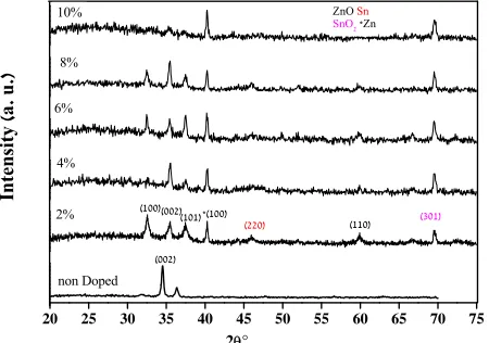
Figure 1 shows the spectra of X-ray diffraction for thin
films of Sn doped and undoped. The peaks of X-ray dif- fraction indicate that all obtained films are polycrystal- line with hexagonal wurtzite structure and a preferential orientation of c axis perpendicular to the substrate. There was no significant difference for the films undoped and Sn doped. Both kinds of spectra represent the dominant peak (002) which is located 2θ = 34.09˚ and 34.55˚, re- spectively. Authors attribute this shift to the substitution of zinc and tin in the hexagonal structure. This result is in good agreement with literature data [13-15]. Another major orientation present is (100) and (101) are also seen in Figure 1.
It is also evident in Figure 1 that the preferential (002)
peak intensity increases with increasing Sn dopant con- centration. This indicates an improvement in films crys-
20 25 30 35 40 45 50 55 60 65 70 75
2°
Int
ens
it
y
(
a
.
u.
)
(101) (100)
non Doped
(002) *(100)
(220) (110) (301) (002)
2% 4% 6% 8%
ZnO SnO2 *Zn
Sn
10%
Figure 1. X-ray diffraction spectra of un-doped and Sn doped ZnO thin films.
tallinity with Sn film doping. However, for concentra- tions above 8% the films crystallinity is degraded [16] with Sn doping and the preferential orientation are changed from (002) to (101) and (100) [17,18]. This dis- crepancy may be due to the difference in the surface re- actions.
The grain size of crystallites was calculated using a well-known Scherrer’s formula [19]:
0.9 cos
D (1) where D is the grain size of crystallite, λ(=1.54059 Å) the wavelength of X-rays used, βthe broadening of dif- fraction line measured at half its maximum intensity in radians and θ is the angle of diffraction. The values of grain size are found to be 31 nm to 41.37 nm for Sn doped ZnO and 29 nm for ZnO non doped thin films.
Figure2 shows the variation of the grain size calculated
from the X-ray diffraction patterns as mentioned in ex- perimental section. The grain size of the films increases with different introduced percentages of the Sn.
3.2. Optical Properties
The optical properties of thin films of ZnO undoped and doped Sn was determined from the transmission meas- urement in the range of 300 - 800 nm. Figure 3 shows
the optical transmission of the doped films deposited onto the glass substrates. The transmission of the films changes with the Sn percentage doping. The properties of the films vary with the percentage of the doping element and this causes light loss on the films. Thus, the changes in the transmission take place. The fundamental absorp- tion edge of the films corresponds to electron transitions from valence band to conduction band and this edge can be used to calculate the optical band gap of the films. The transmission decreases slightly when the percentage of Sn increases. All films show a high transmission in the UV-Vis and with a sharp absorption edge at 380 nm.
0 2 4 6 8 10
28 32 36 40
G
rain size
(nm)
Doping level (%wt)
[image:2.595.61.286.546.704.2]300 400 500 600 0
10 20 30 40 50 60 70 80 90 100
700 800
Transm
is
sion T(%
)
Wavelength (nm)
[image:3.595.67.277.83.248.2]2% Sn 4% Sn 8% Sn 6% Sn 10% Sn 0% Sn
Figure 3. The transmittance spectra of un-doped and Sn doped ZnO thin films.
The absorption coefficient α of ZnO films was deter- mined from transmittance measurements. The films ab- sorption coefficient was calculated using the following expression:
1 d ln T
(2) where T is the normalized transmittance and d is the film thickness. These absorption coefficient values were used to determine optical energy gap. The energy gap (Eg) was estimated by assuming a direct transition between valence and conduction bands from the expression:
1 2h Eg
h A
(3) where A is a constant, hv is the photon energy and Eg is the optical band. Figure 4 shows plots of (αhv)2 versus
(hv). The optical band gap of the films was calculated from these plots.
The Optical energy gap was derived assuming a direct transition between the edges of the valence band and the conduction band. The plot of (αhν)2 versus (hν) gives by
extrapolation of the linear region of the resulting curve the optical band gap value.
The calculated optical gap of samples increases with increasing the percentage of Sn from 3.256 eV for un- doped ZnO films to 3.3 eV for ZnO doped Sn. This shift of absorption of nanocrystalline films of ZnO doped Sn can be explained by the Burstein-Moss effect [20] while assuming the increase in carrier concentration that blocks the lowest states in the conduction band.
The absorption coefficient of films shows a tail for subband gap photon energy; this tail is so-called Urbach tail. The latter, which is closely related to the disorder in the film network, is expressed as [20]:
exp h E U 0
(4) where α0 is a constant, EU is the Urbach energy, which
characterizes the slope of the exponential edge. The
above equation describes the optical transition between occupied state in the valence band tail to unoccupied state of the conduction band edge. Figure 5 shows Ur-
bach plots of the films. The value of EU was obtained
from the inverse of the slope of lnα versus (hν). EU val-
ues change inversely with optical band gap.
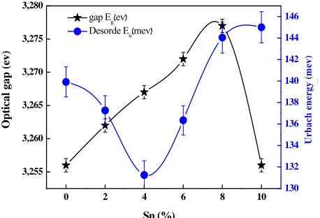
Figure 6 shows the variations of the optical gap to-
gether with the Urbach tail energy as a function of Sn doping level. It is clear that the optical gap is reduced with Sn doping. This band gap narrowing is due to the increase in the band tail width as shown in Figure 6. It is
worth to bear in mind that the Urbach tail energy is closely related to the disorder in the film network. Since the ion radius of Sn is larger than Zn [20], the Sn intro- duction into the films is then followed by the lattice dis- tortion and consequently disorder creation which cause the optical reduction. The same conclusion has been re- ported by A. Hafdallah et al. [11] in In doped ZnO.
[image:3.595.311.533.363.518.2]The optical gap increases with the Sn doping concen- tration up to the percentage of 8%. Above this doping level, the gap value decreases. This shows that the per- centage of 8% is the solubility limit of Sn in ZnO.
[image:3.595.314.535.556.717.2]Figure 4. The plots of (αhν)2 as function of photon energy of the ZnO doped Sn.
0 2 4 6 8 3,255 3,260 3,265 3,270 3,275 3,280 10 gap Eg(ev)
Desorde Eu(mev)
Sn (%)
O
p
tical gap (ev)
130 132 134 136 138 140 142 144 146 Do r d e E
閟
[image:4.595.59.288.86.242.2]ev ) u (m U rb a ev ) ch e n erg y (m
Figure 6. The effect Sn dopant on optical band gap and Urbach energy of the films.
4. Conclusions
ZnO thin films were deposited by ultrasonic spray tech- nique with a non aqueous solution. The effect of Sn con- centration on the structural and optical properties of films was investigated. The deposited films of ZnO undoped and doped Sn showed that the films have polycrystalline structure witch preserve their (002) preferential orienta- tion. The grain sizes increased depending on the increas- ing Sn concentration.
The optical transmission increases and becomes im- portant for > 380 nm, which proves that the ZnO thin films Sn doped have an excellent transparency in the visible game while the optical gap is reduced with in- creasing in Sn/Zn doping ratio. This is linked to the dis r with incorporation Sn in the film.
The optical gap of ZnO films increases with the per- centage of Sn doping. When the limit of 8% doping is reached, the gap is reduced.
REFERENCES
[1] J. B. Baxter and E. S. Aydil, “Dye-Sensitized Solar Cells Based on Semiconductor Morphologies with ZnO Nano- wires,” Solar Energy Materials and Solar Cells, Vol. 90, No. 5, 2006, pp. 607-622.
doi:10.1016/j.solmat.2005.05.010
[2] S. T. Shishiyanu, T. S. Shishiyanu and O. I. Lupan, “Sensing Characteristics of Tin-Doped ZnO Thin Films as NO2 Gas Sensor,” Sensors and Actuators B: Chemical,
Vol. 107, No. 1, 2005, pp. 379-386. doi:10.1016/j.snb.2004.10.030
[3] J. M. Szarko, J. K. Song, B C. W. lackledge, I. Swart, S. R. Leone, S. Li, et al., “Optical Injection Probing of Sin-gle ZnO Tetrapod Lasers,” Chemical Physics Letters, Vol. 404, No. 1-3, 2005, pp. 171-176.
doi:10.1016/j.cplett.2005.01.063
[4] T. Ootsuka, Z. Liu, M. Osamura, Y. Fukuzawa, R. Kuroda, Y. Suzuki, et al., “Studies on Aluminum-Doped ZnO Films for Transparent Electrode and Antireflection
Coating of β-FeSi2 Optoelectronic Devices,” Thin Solid
Films, Vol. 476, No. 1, 2005, pp. 30-34. doi:10.1016/j.tsf.2004.06.145
[5] X. Yu, J. Ma, F. Ji, Y. Wang, X. Zhang and H. Ma, “In- fluence of Annealing on the Properties of ZnO: Ga Films Prepared by Radio Frequency Magnetron Sputtering,”
Thin Solid Films, Vol. 483, No. 1-2, 2005, pp. 296-300. doi:10.1016/j.tsf.2005.01.013
[6] J. Ma, F. Ji, D. Zhang, H. Ma and S. Li, “Optical and Electronic Properties of Transparent Conducting ZnO and ZnO: Al Films Prepared by Evaporating Method,” Thin Solid Films, Vol. 357, No. 2, 1999, pp. 98-101.
doi:10.1016/S0040-6090(99)00357-0
[7] D. A. Lamb and S. J. C. Irvine, “Growth Properties of Thin Film ZnO Deposited by MOCVD with n-Butyl Al-cohol as the Oxygen Precursor,” Journal Crystal Growth, Vol. 273, No. 1-2, 2004, pp. 111-117.
doi:10.1016/j.jcrysgro.2004.08.027
[8] J. Zou, S. Zhou, C. Xia, Y. Hang, J. Xu, S. Gu, et al., “Structural Optical and Electrical Properties of ZnO Films Grown on c-Plane Sapphire and (1 0 0)γ-LiAlO2
by Pulse Laser Deposition,” Journal Crystal Growth, Vol. 280, No. 1-2, 2005, pp. 185-190.
doi:10.1016/j.jcrysgro.2005.03.036
[9] P. Nunes, E. Fortunato, P. Tonello, F. Braz Fernandez, P. Vilarinho and R. Martins, “Effect of Different Dopant Elements on the Properties of ZnO Thin Films,” Vacuum, Vol. 64, No. 3-4, 2002, pp. 281-285.
doi:10.1016/S0042-207X(01)00322-0
[10] A. A. EL-Fadl, G. A. Mohamed, A. B. Abd EL-Moiz and M. Rashad, “Optical Constants of Zn1−xLixO Films Pre-pared by Chemical Bath Deposition Technique,” Physica B: Condensed Matter, Vol. 366, No. 1-4, 2005, pp. 44-54. [11] A. Hafdallah, F. Yanineb, M. S. Aida and N. Attaf, “In
Doped ZnO Thin Films,” Journal of Alloys and Com- pounds, Vol. 509, No. 26, 2011, pp. 7267-7270.
doi:10.1016/j.jallcom.2011.04.058
[12] M. A. Lucio-Lópeza, M. A. Luna-Arias, A. Maldonado, M. de la L. Olvera and D. R. Acosta, “Preparation of Conducting and Transparent Indium-Doped ZnO Thin Films by Chemical Spray,” Solar Energy Materials and Solar Cells, Vol. 90, No. 6, 2006, pp. 733-741.
doi:10.1016/j.solmat.2005.04.010
[13] Y. Caglar, S. Ilican, M. Caglar and F. Yakuphanoglu, “Effects of Al and Sn Dopants on the Structural and Op-tical Properties of ZnO Thin Films,” Spectrochimica Acta Part A, Vol. 67, No. 3-4, 2007, pp. 1113-1119.
[14] J.-H. Lee and B.-O. Park, “Characteristics of Al-doped ZnO Thin Films Obtained by Ultrasonic Spray Pyrolysis Effects of Al Doping and an Annealing Treatment,” Thin Solid Films, Vol. 426, No. 1-2, 2003, pp. 94-99. doi:10.1016/S0040-6090(03)00014-2
[15] Z.-Q. Xu, H. Deng, Y. Li and H. Cheng, “Al-Doping Effects on Structure, Electrical and Optical Properties of c-Axis-Orientated ZnO: Al Thin Films,” Materials Sci- ence in Semiconductor Processing, Vol. 9, No. 1-3, 2006, pp. 132-135. doi:10.1016/j.mssp.2006.01.082
and Characterization,” Journal of Optoelectronics and Advanced Materials, Vol. 10, No. 10, 2008, pp. 2592- 2598
[17] S. Ilican, Y. Caglar, M. Caglar and F. Yakuphanoglu, “Electrical Conductivity, Optical and Structural Proper- ties of Indium-Doped ZnO Nanofiber Thin Film Depos- ited by Spray Pyrolysis Method,” Physica E: Low-Di- mensional Systems and Nanostructures, Vol. 35, No. 1, 2006, pp. 131-138. doi:10.1016/j.physe.2006.07.009 [18] M. A. Kaid and A. Ashour, “Preparation of ZnO-Doped
Al Films by Spray Pyrolysis Technique,” Applied Surface
Science, Vol. 253, No. 6, 2007, pp. 3029-3033. doi:10.1016/j.apsusc.2006.06.045
[19] B. D. Cullity and S. R. Stock, “Elements of X-Ray Dif- fraction,” 3rd Edition, Prentice Hall, Upper Saddle River, 2001.