Abstract— We have investigated the impact of circuit limitations on the design of an Asynchronous Sigma-Delta Modulator (ASDM). Specifically, the hysteresis, which is normally embedded during the quantization process, can be used to improve the performance of ASDM. A programmable hysteretic element was designed and implemented for the quantizer and tested in an ASDM circuit based on John G. Harris et. al. We have shown that modulating the hysteresis in the quantizer can provide a larger input frequency range and save power for low-frequency signal conversion. This circuit converts signals up to 2MHz and 83% of the switching power is saved by switching to a larger hysteresis mode at low frequencies. By following the Harris structure, the design eliminates the op-amp based structure, which is also considered a significant bottleneck for energy efficiency in ADC implementations. The circuit was designed in AMI’s 0.6μm 5-V process.
Index Terms—Asynchronous sigma-delta modulator, hysteresis, analog-to-digital convertor, switching rate.
I. INTRODUCTION
The Sigma-Delta modulator is one of the most popular implementations for Analog to Digital converters due to its special features such as oversampling and noise shaping. One of the recent and most promising developments in this field is the asynchronous Sigma-Delta modulator proposed and implemented by John G Harris [1], which uses no clocks of any kind, thereby avoiding the clock jitter inherent in continuous-time implementation. This implementation uses simple circuits, eliminating the op-amps required by the switch capacitor circuits in discrete time implementations and gives promise for a high speed, low power implementation [2].
Manuscript received July 26, 2009.
Pingyun. Wei. Author, is with Rose-Hulman Institute of Technology, Terre Haute, IN 47803 USA. (e-mail: [email protected]).
Tina. A. Hudson is with the Electrical and Computer Engineering Department, Rose-Hulman Institute of Technology, Terre Haute, IN 47803 USA(e-mail: [email protected]).
Based on the perfect reconstruction theory proposed by Lazar and Toth [3], a clockless system should be able to produce a recoverable conversion of the input signal. Perfect reconstruction theory suggests that “a time sequence output, containing information of input can be recovered without loss of information if any two consecutive values of the time sequence is bounded by the inverse of the Nyquist rate.”[3] If this condition is met, the output sequence of the asynchronous Sigma-Delta modulator is promised to reconstruct the input signal after it goes through a time to digital converter. [4]
Ideally, a system without a clock control will result in an infinite switching rate at the output; however, due to finite propagation delay, system loop delay, leakage current at the integrator, and hysteresis at the quantizer, delays are inevitable, which results in an effective switching rate. The maximum value of this switching rate, which is also called the limit cycle, is the major part of evaluating the performance of ASDM circuits [5]. With consideration of all the circuit limitations mentioned above, a higher switching rate is critical for high frequency input signals to meet perfect reconstruction requirement, however, not necessary for low frequency input signals. The impact of system loop delay time, which causes nonlinearities in the system, will be less significant for a lower switching rate while obtaining the desired system performance. Additionally, the switching power is greatly reduced at lower frequency input signals sampled at a lower effective switching rate.
Based on our theory, we have designed a modification of the Harris et. al. single-bit asynchronous Sigma-Delta modulator to include control of the hysteretic element to modify the switching rate. Because the loop delay is sensitive to parasitic capacitances, we performed the layout so that impact of these elements would be included in the simulations. The circuit was designed for minimum delay to allow for high frequency conversion and can be placed in three different modes by the control element in the quantizer. Each mode exhibits a different level of hysteresis and thereby different power savings. Simulations in each region showed a SNR of at least 20 dB and a power savings of 83 % between the highest frequency and lowest frequency modes.
Performance Improvement of an Asynchronous
Sigma-Delta Modulator by Programmable
Hysteresis
II. CIRCUIT LIMITATIONS ANALYSIS
Fig 1 shows a realistic system implementation for an ASDM including the circuit limitations mentioned above. In the integration process, Gm is the trans-conductance, C is the capacitance, R is the output resistance
Figure 1: System diagram of a single bit ASDM
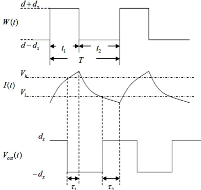
In order to simplify the analysis, a constant signal with amplitude of
d
(−
d
x<
d
<
d
x) is applied at the input. Fig 2 shows the circuit operation at each stage.Figure 2: Time-domain illustration of the operation of ASDM with dc input
d
Fig. 2 shows how the integrator and quantizer produce a periodic pulse modulated signal with period of T at the output (Vout(t)).
τ
1andτ
2are system delays, which varies from designs and manufacturing.A. Leakage current
If system delay is ignored, the impact of the integrator and quantizer on the output can be mathematically approximated as follows.
h=Vh−Vl (1)
2 ) ( t1
h dx d GmR
RCh
− +
= (2)
2 ) (
2 h
d dx GmR
RCh t
− −
= (3)
The average of the output is calculated in (4).
d
h GmR d
GmR t
t t t
x
• − =
+ −
2 2
2 1
2
1 (4)
Equations (2)-(4) indicate that the time interval
t
1 andt
2is slightly influenced by the output resistance of the integrator, resulting in a leaky integrator; however the signal can be perfectly recovered with some scaling value.
B. System Loop Delay
If the system delay is included in the previous analysis, the average of the output is no longer linearly proportional to input signal d except when the switching down delay
τ
1is equal to switching up delayτ
2.C. Hysteresis
From (1)-(3), we can see that smaller time constant for the integrator, larger amplitude of D/A output , and smaller
h
will decrease the adjacent time interval of the output, thus increase the switching rate. However, a larger amplitude of the D/A output,
d
x, will decrease the scaling factor of the average output resulting in a negative impact on the system SNR. Hysteresis, which is embedded in the quantizer, is the best way to control the switching rate.In this section, we have shown that the leakage current, system loop delay, and hysteresis (represented by the distance of
V
l andV
h) are the major keys to controlling the switching rate and how these circuit limitations impact the performance of ASDM. By investigating each of these components of the system, we found that modifying the hysteresis is the best method of changing the switching rate of the ASDM.III. CIRCUIT IMPLEMENTATION
Figure 3: Circuit diagram of ASDM A. Integrator
To design the integrator, the design process presented in Harris et. al. was followed. A GM-C filter was chosen to implement the integrator because of its simple circuitry which provides less delay and a large linear region.
Figure 4: Circuit implementation of Integrator
The basic operation of the integrator follows. M5 and M6 (see Fig. 4) work in the triode region, acting like a resistor, to provide linearity. Vb0 sets the bias current I for the input common mode voltage, and M15-M18 sets the bias current for the output common mode voltage. Since transistor sizes are carefully chosen to make sure M5 and M6 are working in the triode region, the drain and source node for M5 and M6, which is also the source node for M9 and M10, are comparably stable. Therefore, M15 can provide a stable bias current. On the other hand, due to the large voltage swing at the drain node for M7 and M8, a wide swing cascode current mirror (created by M11-M14) is needed so that the current through M9 can be accurately mirrored to M12. The Gm value, under the assumption that
V
ds5<<
V
sg5−
V
thp , can be calculated as shown below [1]:
7 3 1 5
2 2
β β β
β I
Gm= (5)
B. Summer
The circuit summer is designed in a similar manner as the integrator. The two output currents are summed and filtered by the capacitor C to avoid a large op-amp based adder with large resistors. Gm2 is designed to provide enough gain for the feedback currents.
C. Quantizer
All system components were designed so that the hysteresis in the quantizer will have a significant impact on setting the switching rate. The core design of this quantizer was taken from Harris et. al.[1]; however, additional elements were added to modify the hysteresis by changing the current provided by the current source.
Figure 5: Circuit implementation of quantizer and D/A
As shown in Fig. 5, different current sources, which connect to W1 and W2 by two switches, are used to program the hysteresis. In Harris et. al., the circuit was implemented with a basic current source. However, due to channel length modulation, large voltage swings caused significant changes in the hysteretic current preventing the hysteresis from being accurately controlled. To solve this problem, the current mirror was replaced with a wide swing cascode current mirror.
17 2 1 17
2
1 ) ( )
(
β β
I I I
I V V
h= rh− rl = + − − (6)
Equation (6) shows that by changing the bias currents
I
1frequency range. However, for low frequency signals, if the delay due to hysteresis no longer dominates adjacent switching time intervals, which introduces nonlinearities, performance can be improved. Additionally, increasing the hysteresis can reduce the switching rate to avoid overly abundant oversampling which is unnecessary for the conversion of low frequency signals. Such a modification significantly reduces the switching power in the system.
Each current source is designed as shown in Fig.6:
Figure 6: Current source design
D. D/A
In Fig 5, a one bit D/A is implemented using a simple circuit that scales the output voltage to the value Vref±A, where A is a scaling factor. Using such a simple circuit results in less system loop delay and transistors are sized properly to produce equal propagation delay for both high and low input signals. A large value of A produces a large input swing for the circuit improving the SNR; however, this also requires a large input linear range for the integrator. Additionally, a large value for A requires more power consumption. This demonstrates the trade-offs associated with this circuit in performance, linearity and power consumption.
IV. EXPERIMENTAL RESULTS
We designed and simulated the circuit based upon the design considerations stated in the previous section. We applied a differential input signal with 100mV amplitude and a 2.5V offset. For the integrator, Vb0 is set to provide a 5uA bias current with a 2.6V common mode output voltage, and a capacitance value of 2pF. For the quantizer, we choose Vref = 2.6 and for the D/A, we choose the scaling factor to be 600mV.
The values of
I
2 andI
1 are designed to change the hysteresis in different hysteretic modes. For two of the modes, hysteresis=0.09 and hysteresis=0.02,I
2was set to a constant value (5uA) andI
1 was adjusted to change the level of hysteresis using eq. (1). However, in the final mode, hysteresis=0.5,I
2 had to be raised to 100uA to obtain theresolution necessary to reach the desired hysteresis level with
1
I
equal to 102uA.A. SNR versus Frequency
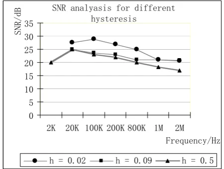
To test the impact of the hysteresis on the performance, we applied various frequencies at the input and by looking at the spectrum of the output signals, calculated the signal-to-noise ratio (SNR) as the ratio of the signal power to the adjacent noise power, assuming the output signal will be reconstructed with a band-pass filter. The test was repeated for different hysteresis levels (specified as h in Fig. 3 and 4) ranging from 0.02 to 0.5.
SNR analyasis for different hysteresis
0 5 10 15 20 25 30 35
2K 20K 100K 200K 800K 1M 2M
Frequency/Hz
SNR
/dB
[image:4.595.311.537.247.417.2]h = 0.02 h = 0.09 h = 0.5
Figure 7: SNR plot for various frequency ranges
The SNR data is presented in Fig. 7.The data shows that the SNR changes with frequency and hysteresis level. As the frequency increases for a given hysteresis level, the loop delay becomes closer to the period of the signal, resulting in less oversampling for the conversion and more of the signal power lost to noise. Similarly, for a given signal frequency, increasing the hysteresis causes a lower switching rate and thereby less oversampling and lower SNR.
With the programmable hysteresis, the system is working for frequencies up to 2MHz compared to John G Harris ’s paper[1], which is up to 6 KHz.
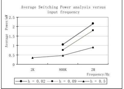
B. Switching Power verses hysteresis
Power consumption was simulated for 3 frequencies at 3 hysteresis levels to show the impact of hysteresis on this specification. Power consumption was determined by measuring the average switching power with the dc offset removed over 1ms.
power to charge and discharge the capacitor to the peak voltages.
The power savings due to hysteresis changes is significant. At 2MHz, the power savings is 58% (0.9mW for h=0.5 and 2.17mW for h=0.02); however this savings has a cost of pushing the SNR below 20dB. However, at 800kHz, the power savings is 54.8%, with both hysteretic levels producing SNR levels greater than or equal to 20dB. Considering the power savings from one hysteretic mode to the next, an 80% power savings is evident between the high frequency, low hysteresis mode and the low frequency, high hysteresis mode. Clearly, by changing the hysteresis levels, a reasonable SNR can be maintained while providing a significant power savings.
Average Switching Power analysis versus input frequency
0 0.5 1 1.5 2 2.5
2K 800K 2M
Frequency/Hz
Ave
rage
Po
wer/
mW
[image:5.595.72.278.271.418.2]h = 0.02 h = 0.09 h = 0.5
Figure 8: Average switching power plot versus input frequency for various hysteresis
V. CONCLUSIONS
In this paper, we investigated the impact of circuit implementations (leakage current, system loop delay and hysteresis) on an asynchronous Sigma-Delta modulator to improve its performance. We also designed a programmable hysteretic element in the quantizer to obtain a larger input frequency range and save power. The simulations indicate that less hysteresis will increase the switching rate on high frequency signals; however, more hysteresis is necessary to make the impact of system loop delay less significant for the system work at lower frequency range, thus improve performance. Further more, while keeping a required SNR, increasing hysteresis can significantly decrease switching power. The circuit is designed and laid out under CMOS Technology and showed a large bandwidth (up to 2MHz) with a SNR at least 20dB. Simulation data showed an 83% power savings when moving from the low hysteresis mode to the high hysteresis mode.
REFERENCE
[1] Dazhi Wei, Vaibhav Garg, Harris, J.G, , “An asynchronous delta-sigma converter implementation.” IEEE International Symposium on Circuit and Systemes (2006): 4 pp.
[2] Hae-Seung Lee, Sodini, C.G, “Analog-to-Digital converters: digitizing the analog world.” Proceedings of the IEEE(2008): 323 – 334.
[3] Aurel A. Lazar, Lasxlo T. Toth Aunet. “Perfect recovery and sensitivity analysis of time encoded bandlimited signals.” IEEE
Transactions on Circuits and Systems (2006): 2006 – 2007
[4] Daniel, J. Dehaene, W, Steyaert, M, Wieshauer, A,. “A/D conversion using an asynchronous Delta-Sigma modultaor and a time-to-digital converter" IEEE International Symposium on Circuit and Systems 16 (2008): 1648-165