1
DEVELOPMENT OF A DOUBLE-INPUT INTERLEAVED
BOOST DC-DC CONVERTER
YONIS. M. YONIS BUSWIG
DEVELOPMENT OF A DOUBLE-INPUT INTERLEAVED BOOST DC-DC CONVERTER
YONIS. M. YONIS BUSWIG
A thesis submitted in
fulfilment of the requirement for the award of the Doctor of Philosophy
Faculty of Electrical and Electronic Engineering Universiti Tun Hussein Onn Malaysia
For my beloved mother and father.
Thank you for your prayer for me whole this time.
I love you very much.
Acknowledgment
"Alhamdulillah", all praise to ALLAH, the most gracious and the most merciful, for all the strength and will provided to the author in completing the research. Without "the mercy", the author is just an ordinary person who may not even understand what the research topic is all about.
The author would like to express utmost appreciation and gratitude to the research supervisor, Dr Wahyu Mulyo Utomo for his guidance, persistent encour-agement and associated aid throughout the research period. His understanding and patience during the tough period are forever appreciated.
Heartiest thanks are due to the senior technician for his full cooperation for the research. Appreciation is also dedicated to those who contributed directly or indirectly towards the success of this thesis.
Finally, sincere thanks are dedicated to the author’s parents and family for their consistent prays, patience and never-ending support. May ALLAH bless all of us.
Last but not least, thank you to all my friends for their helps, criticisms and ideas. Also, to LYX developers all over the world, thank you for this useful document processor that helped me a lot for a nice formatting thesis writing.
Abstract
Suitable integration of several energy sources profoundly depends on the power electronic converters which interface multiple energy sources that having different characteristics. Conventionally, multiple sources are connected either in series or parallel configurations. However, these configurations have disadvantages such as having difficulty to achieve regulated output voltage and produce high ripples. Consequently, it is more beneficial to use a multi-input converter rather than several independent converters, as it results in less components, simpler control, more stability, and also lower ripples. In this research, a double-input boost DC-DC converter (DIBC) is proposed using the concept of pulsating voltage source cells (PVSCs) for synthesis and generation of input sources circuit combined with double inductors interleaved concept as ripple reduction technique in order to re-duce the current ripple. The proposed double-input converter is composed of two voltage sources that accommodated with converter cell and the conduction of interleaving switches decides the interleaved operating mode and boosting level. Different operating modes of the proposed converter are obtained as well as its corresponding voltage ratios are derived. In the controller design, a Pulse Width Modulation (PWM) technique is used to control the commuting switches while the neural network (NN) control algorithm is used to manage and regulate out-put voltage of the proposed DIBC. The NN controller is trained by the online back propagation algorithm to achieve output voltage regulation despite vari-ations in line voltage and the load; as well output voltage tracking capability. The proposed DIBC system has been investigated through simulation using the MATLAB/Simulink environment and validated experimentally on a laboratory prototype using DSP TMS320F28335 real-time digital controller. The conducted simulation and experiments obtained good results for low ripples and voltage regulation.
Abstrak
Contents
Declaration ii
Dedication iii
Acknowledgment iv
Abstract v
Abstrak vi
List of Figures xi
List of Tables xx
List of Appendices xxi
List of Nomenclatures xxii
Chapter 1 Introduction 1
1.1 Introduction 1
1.2 Research Background 1
1.3 Problem Statements 3
1.4 Research Objective 3
1.5 Research Scope 4
1.6 Research Methodology 4
1.7 Thesis Outline 5
Chapter 2 Literature Review 7
2.1 Introduction 7
2.2 Overview of Basic DC-DC Converters 7
2.2.1 Basic DC Power Converter System 7
2.2.2 Basic Circuit of DC–DC Converter 8
2.2.3 Basic Operation Modes of DC–DC Converter 10 2.2.4 Basic Elements of DC-DC Converter 11 2.2.5 Basic Switching Frequency of DC-DC Converter 12 2.2.6 Basic Voltage Regulation of DC-DC Converter 13 2.3 Overview of Multiple-input DC-DC Converter System 14 2.3.1 Parallel-Single Input Converters 15
2.3.2 Series-Single Input Converters 16
2.3.3 Multi-input Converter System 16
2.4 Review of Multi-Input DC-DC Converters 17 2.4.1 Previous Works of Isolated Multi-Input
DC-DC Converters 17
2.4.2 Previous Works of Non-Isolated Multi-Input
DC-DC Converters 22
2.5 Review of Control Methodologies of DC-DC Converters 28
2.5.1 Adaptive Control 28
2.5.2 Fuzzy Logic Control 30
2.5.3 One-Cycle Control 31
2.5.4 Sliding Mode Control 32
2.5.5 Artificial Neural Network Control 34 2.6 Review of Control Methodologies of Multi-input
DC-DC Converters 35
2.7 Gap of Study 36
2.8 Summary 37
Chapter 3 Methodology 38
3.1 Introduction 38
3.2 Configuration of the Proposed Double-input
DC-DC Converter 38
3.3 Circuit of the Proposed Double-input Boost Converter 39 3.3.1 The Proposed Double-input Circuit 40
3.3.2 The Proposed LC Filter Circuit 41
3.4 Switching Patterns for Proposed Double-input
Boost Converter 42
3.4.1 Decision of Duty Ratio for Main Switches 42 3.4.2 Decision of Duty Ratio for Interleaving Switches
and Number of Phases 43
3.5 Components Selection of the Proposed
Double-Input Boost Converter 44
3.5.2 Design and Selection of Output Filter 46 3.6 Operating Principle of the Proposed Double-Input
DC-DC Converter 46
3.7 Voltage Transfer Ratio of the Proposed
Double-Input DC-DC Converter 51
3.8 Proposed Control of Double-Input DC-DC Converter 53 3.8.1 Block Diagram of Proposed Control 53 3.8.2 Design of Proposed Neural Network Control 54
3.8.2.1 Structure of Proposed Neural
Net-work Controller Algorithm 54
3.8.2.2 Learning Algorithm of Back propagation 55
3.9 Summary 57
Chapter 4 Research Design and Results 58
4.1 Introduction 58
4.2 Comparative Studies on Conventional
Double-input DC-DC Conveter 58
4.3 Overview of Proposed System Development 100 4.4 Simulation Model of the Proposed Double-Input
Boost Converter 101
4.4.1 Open-Loop Simulation Model 101
4.4.2 Open-Loop Simulation Results 103
4.4.2.1 Matched Input Voltage Sources 103 4.4.2.2 Mismatched Input Voltage Sources 106 4.4.2.3 Voltage Regulation Capability 114
4.4.3 Closed-Loop Simulation Model 118
4.4.3.1 Closed-Loop Simulation Results 119 4.4.3.2 Line Regulation Capability 119 4.4.3.3 Load Regulation Capability 120 4.4.3.4 Voltage Regulation Capability 121 4.5 Hardware Development and Implementation 129
4.5.1 Prototype Design of the Proposed
Double-Input Circuit 130
4.5.2 Integration of MATLAB Model with Pro-totype circuit of Proposed Double-Input
Converter 130
4.5.3 Experimental Set-up of the Double-input
Boost Converter Circuit 132
4.5.4 Experimental Results 132
4.5.4.1 Open-Loop Experimental Results 133 4.5.4.2 Matched Input Voltage Sources 133 4.5.4.3 Mismatched Input Voltage Sources 136 4.5.4.4 Voltage Regulation Capability 141 4.5.4.5 Closed-loop Experimental Results 142 4.5.4.6 Line Regulation Capability 142 4.5.4.7 Load Regulation Capability 143 4.5.4.8 Voltage Regulation Capability 144 4.6 Performance Analysis of the Proposed Design 152
Chapter 5 Conclusion and Future Work 154
5.1 Conclusion 154
5.2 Future Work 156
References 157
List of Figures
Figure No Title Page
2.1 Block diagram of a DC power converter system (Liu
& Lee, 1988). 8
2.2 Basic DC–DC converter topologies (Liu & Lee, 1988). 9 2.3 Typical inductor current waveform of the DC-DC
con-verters (Mitchell, 1988). 11
2.4 Equivalent circuit of voltage mode control (Liu & Lee, 1988). 14 2.5 Parallel-connected converter (Camara et al., 2006). 15
2.6 Series-connected converters (Camaraet al., 2006). 16
2.7 Photovoltaic system using a multi-input converter
(Ca-mara et al., 2006). 17
2.8 Multi-input flyback DC-DC converter (Zhao et al., 2008). 18
2.9 Isolated multi-input boost half-bridge DC-DC
con-verter (Tao et al., 2008b). 19
2.10 Isolated multi-input boost full-bridge converter (Tao
et al., 2008b). 19
2.11 Isolated multiple-input with two full-bridge DC-DC
converter (Chen et al., 2001). 20
2.12 Isolated multiple-input ZVS bidirectional DC-DC
con-verter (Caricchi et al., 1993). 21
2.13 High step-up multi-input bidirectional isolated
con-verter (Liu & Li, 2005). 21
2.14 Multi-input converters derived from H-bridge
struc-ture (Ahmadi & Ferdowsi, 2012). 22
2.15 Multiple input DC-DC converter with
battery/ultra-capacitor (Li et al., 2009). 23
2.16 Multi-Input Z-Source DC-DC converter (Sedaghati &
Babaei, 2011). 24
[image:11.595.129.525.231.746.2]2.17 Multiple-input with four-phase bidirectional flyback
converter (Bhattacharya et al., 2009). 24
2.18 Extendable single-stage multi-input DC–DC/AC boost
converter (Danyali et al., 2014). 25
2.19 A non-isolated multi-input DC–DC buck–boost
con-verter (Kwasinski, 2009). 25
2.20 Integrated multi-input buck-buckboost converter
(Be-navides & Chapman, 2005). 26
2.21 Integrated buckboost-buckboost converter
(Yalaman-chiliet al., 2006). 27
2.22 Multile-input SEPIC converter (Kwasinski, 2009). 27 2.23 Multiple-input Cuk converter (Kwasinski, 2009). 28 2.24 An adaptive control system (Tse & Adams, 1990). 29 2.25 Fuzzy logic control system (So et al., 1996). 30
2.26 One-cycle control system (Smedley & Cuk, 1995). 31 2.27 Sliding mode control system (Bilalovic et al., 1983). 33
2.28 Neural network control system (Chan et al., 1993). 34
3.1 General block diagram of the proposed double-input
DC-DC converter. 39
3.2 The proposed double-input boost converter circuit. 40
3.3 The proposed double-input circuit. 40
3.4 The two interleaved inductors L1 and L2. 41
3.5 Input current with inductors current operating out of phase. 42 3.6 Switching pattern of main switches S1 and S2. 43 3.7 Switching pattern of interleaving switches S3 and S4. 44
3.8 Circuit diagram of the proposed converter. 47
3.9 Switching patterns and current waveforms of the
pro-posed converter. 47
3.10 OperatingM ode I at timet1. 48
3.11 OperatingM ode II at timet2. 49
3.12 OperatingM ode III at time t3. 49
3.13 OperatingM ode IV at timet4. 50
3.14 Block diagram of voltage controller design. 53 3.15 Architecture of the proposed neural network controller. 54
4.1 Circuit diagram of double-input boost converter. 59 4.2 Simulation model circuit of double-input boost converter. 59
4.3 Total input current waveform. 60
4.5 Output current waveform. 61
4.6 Ripple of output current waveform. 62
4.7 Output voltage waveform. 62
4.8 Ripples of output voltage waveform. 63
4.9 Resulted ripples of output voltage waveforms due to
its double-input voltage sources. 63
4.10 Circuit diagram of double-input boost converter. 65 4.11 Simulation model circuit of double-input boost converter. 65
4.12 Total input current waveform. 66
4.13 Ripples of total input current waveform. 66
4.14 Output current waveform. 67
4.15 Ripples of output current waveform. 67
4.16 Output voltage waveform. 68
4.17 Ripples of output voltage waveform. 68
4.18 Resulted ripples of output voltage waveforms due to
its double-input voltage sources. 69
4.19 Circuit diagram of double-input buck converter. 70 4.20 Simulation model circuit of double-input buck converter 71
4.21 Total input current waveform. 72
4.22 Ripples of total input current waveform. 72
4.23 Output current waveform. 73
4.24 Ripples of output current waveform. 73
4.25 Output voltage waveform. 74
4.26 Ripples of output voltage waveform. 74
4.27 Resulted ripples of output voltage waveforms due to
its double-input voltage sources. 75
4.28 Circuit diagram of double-input buck converter. 76 4.29 Simulation model circuit of double-input buck converter. 77
4.30 Total input current waveform 78
4.31 Ripples of total input current waveform. 78
4.32 Output current waveform 79
4.33 Ripples of output current waveform 79
4.34 Output voltage waveform 80
4.35 Ripples of output voltage waveform 80
4.36 Resulted ripples of output voltage waveforms due to
its double-input voltage sources 81
4.37 Circuit diagram of double-input buck-boostconverter. 82 4.38 Simulation model circuit of double-input buck-boost
converter. 83
4.39 Total input current waveform. 84
4.40 Ripples of total input current waveform. 84
4.41 Output current waveform. 85
4.42 Ripples of output current waveform. 85
4.43 Output voltage waveform. 86
4.44 Ripples of output voltage waveform. 86
4.45 Resulted ripples of output voltage waveforms due to
its double-input voltage sources. 87
4.46 Circuit diagram of double-input buck-boost converter 88 4.47 Simulation model circuit of double-input buck-boost
converter 89
4.48 Total input current waveform 90
4.49 Ripples of total input current waveform 90
4.50 Output current waveform 91
4.51 Ripples of output current waveform 91
4.52 Output voltage waveform. 92
4.53 Ripples of output voltage waveform 92
4.54 Resulted ripples of output voltage waveforms due to
its double-input voltage sources 93
4.55 Circuit diagram of double-input Z-aource converter 94 4.56 Simulation model circuit of double-input Z-source converter 95
4.57 Total input current waveform 96
4.58 Ripples of total input current waveform 96
4.59 Output current waveform 97
4.60 Ripples of output current waveform 97
4.61 Output voltage waveform 98
4.62 Ripples of output voltage waveform 98
4.63 Resulted ripples of output voltage waveforms due to
its double-input voltage sources 99
4.64 Block diagram for overall proposed DIBC. 101
4.65 Open-loop simulation model of the proposed
double-input converter circuit using MATLAB Simulink software. 102
4.66 Simulation model of PWM generator block. 102
4.67 Switching signals of switches S1, S2, S3 and S4; [d1 =
d2 = 0.75;d3 =d4 = 0.5]. 103 4.68 Inductors voltage (VL1 and VL2); inductors current
(IL1 and IL2); [d1 =d2 = 0.75;d3 =d4 = 0.5]. 104
4.69 Voltage input source (V in1 andV in2); output voltage
4.70 Output current Iout and output voltage Vout in the
case matched input voltage sources. 106
4.71 Switching signals of switches S1, S2, S3 and S4 [d1 =
d2 = 0.75;d3 =d4 = 0.5]. 107 4.72 Inductors voltage (VL1 and VL2); inductors current
(IL1 and IL2) [d1 =d2 = 0.75;d3 =d4 = 0.5]. 107
4.73 Voltage input source (V in1 andV in2); output voltage
(Vout); total inductor current (IL1+IL2). 108
4.74 Output current Iout and output voltage Vout in the
case mismatched input voltage sources. 109
4.75 Total input current waveform 110
4.76 Ripples of total input current waveform 110
4.77 Output current waveform 111
4.78 Ripples of output current waveform 111
4.79 Output voltage waveform 112
4.80 Ripples of output voltage waveform 112
4.81 Resulted ripples of output voltage waveforms due to
its double-input voltage sources. 113
4.82 Voltage regulation capability of the proposed converter when the output voltage is commanded from 0V to
40V. 115
4.83 Current regulation capability of the proposed con-verter when the output voltage is commanded from
0V to40V. 116
4.84 Voltage regulation capability of the proposed converter when the output voltage is commanded from 0V to
60V. 117
4.85 Current regulation capability of the proposed con-verter when the output voltage is commanded from
0V to60V. 117
4.86 Closed-loop simulation model of the proposed
double-input boost converter. 118
4.87 Simulation model of neural network controller using
MATLAB Simulink software. 119
4.88 Line regulation capability of the proposed double-input converter when input source 1 is stepped down from
24V to 18V. 120
4.89 Load regulation capability of the proposed double-input converter when the load resistance is stepped
down from 10Ω to5Ω. 121
4.90 Voltage regulation capability of the proposed converter with single reference testing when the output voltage
is commanded from 0V to 40V. 122
4.91 Voltage regulation capability of the proposed converter with single reference testing when the output voltage
is commanded from 0V to 60V. 122
4.92 The dynamic response of the proposed double-input converter when the output voltage is commanded to
step up from 0V to36V to45V. 123
4.94 The dynamic response of the proposed double-input converter when the output voltage is commanded to
step up from 0V to36V to50V. 124
4.93 The dynamic response of the proposed double-input converter when the output voltage is commanded to step up from 0V to45V then step down from45V to
36V. 124
4.95 The dynamic response of the proposed double-input converter when the output voltage is commanded to
step up from 0V to50V then step down50V to36V. 125 4.96 The dynamic response of the proposed double-input
converter when the output voltage is commanded to
step up from 0V to40V to50V. 125
4.97 The dynamic response of the proposed double-input converter when the output voltage is commanded to step up from 0V to50V then step down from50V to
40V. 126
4.99 The dynamic response of the proposed double-input converter when the output voltage is commanded to step up from 0V to60V then step down from60V to
45V. 126
4.98 The dynamic response of the proposed double-input converter when the output voltage is commanded to
step up from 0V to45V to60V. 127
4.100 The dynamic response of the proposed double-input converter when the output voltage is commanded to
4.101 The dynamic response of the proposed double-input converter when the output voltage is commanded to step up from 0V to70V then step down from70V to
55V. 128
4.102 The dynamic response of the proposed double-input converter when the output voltage is commanded to
step up from 0V to60V to80V. 128
4.103 The dynamic response of the proposed double-input converter when the output voltage is commanded to step up from 0V to80V then step down from80V to
60V. 129
4.104 Prototype of the proposed double-input converter
cir-cuit. 130
4.105 Integration of MATLAB Tools for DSP Code
Gener-ation block diagram. 131
4.106 Simulink circuit of close loop circuit using MATLAB
Simulink software. 131
4.107 The experimental set-up of the proposed double-input
converter. 132
4.108 Gate pulses of switches S1, S2, S3 and S4 (Ch1, Ch2,
Ch3 and Ch4); [d1 =d2 = 0.75;d3 =d4 = 0.5]. 133 4.109 Inductors voltageVL1 and VL2 (Ch1 and Ch2);
Induc-tors current IL1 and IL2 (Ch3 and Ch4). 134
4.110 Voltage input source V in1 and V in2 (Ch1 and Ch2); output voltage Vout (Ch3); total input inductor
cur-rent IL1+IL2(Ch4). 135
4.111 Average output voltage Vout (Ch3); average output
current Iout (Ch4) in the case matched input voltage
sources. 136
4.112 Gate pulses of switches S1, S2, S3 and S4 (Ch1, Ch2,
Ch3 and Ch4); [d1 =d2 = 0.75;d3 =d4 = 0.5]. 137 4.113 Inductors voltageVL1 and VL2 (Ch1 and Ch2);
Induc-tors current IL1 and IL2 (Ch3 and Ch4). 137
4.114 Voltage input source V in1 and V in2 (Ch1 and Ch2); output voltage Vout (Ch3); total input inductor
cur-rent IL1+IL2 (Ch4). 138
4.115 Average output voltage Vout (Ch3); average output
current Iout (Ch4). 139
4.116 Conventional double-input boost converter: switching signals of switches S1 and S3 (Ch1); switching signal
of switch S2 (Ch2) and output voltage Vout (Ch4). 140
4.117 Proposed double-input converter: switching signals of switchesS3andS4(Ch1 and Ch2); and output voltage
Vout (Ch4). 140
4.118 Voltage regulation capability of the proposed converter when the output voltage is commanded from 0V to
40V. 141
4.119 Voltage regulation capability of the proposed converter when the output voltage is commanded from 0V to
60V. 142
4.120 Line regulation capability of the proposed double-input
converter. 143
4.121 Load regulation capability of the proposed
double-input interleaved boost converter. 144
4.122 Voltage regulation capability of the proposed converter with single reference testing when the output voltage
is commanded from 0V to 40V. 145
4.123 Voltage regulation capability of the proposed converter with single reference testing when the output voltage
is commanded from 0V to 60V. 145
4.124 The dynamic response of the proposed double-input converter when the output voltage is commanded to
step up from 0V to36V to45V. 146
4.125 The dynamic response of the proposed double-input converter when the output voltage is commanded to step up from 0V to45V then step down from45V to
36V. 147
4.126 The dynamic response of the proposed double-input converter when the output voltage is commanded to
step up from 0V to36V to50V. 147
4.128 The dynamic response of the proposed double-input converter when the output voltage is commanded to
step up from 0V to40V to50V. 148
4.127 The dynamic response of the proposed double-input converter when the output voltage is commanded to
4.129 The dynamic response of the proposed double-input converter when the output voltage is commanded to step up from 0V to50V then step down from50V to
40V. 149
4.130 The dynamic response of the proposed double-input converter when the output voltage is commanded to
step up from 0V to45V to60V. 149
4.132 The dynamic response of the proposed double-input converter when the output voltage is commanded to
step up from 0V to55V to70V. 150
4.131 The dynamic response of the proposed double-input converter when the output voltage is commanded to step up from 0V to60V then step down from60V to
45V. 150
4.133 The dynamic response of the proposed double-input converter when the output voltage is commanded to step up from 0V to70V then step down from70V to
55V. 151
4.134 The dynamic response of the proposed double-input converter when the output voltage is commanded to
step up from 0V to60V to80V. 151
4.135 The dynamic response of the proposed double-input converter when the output voltage is commanded to step up from 0V to80V then step down from80V to
60V. 152
E.1 DSP TMS320F28335 real time digital controller. 183
E.2 Functional block diagram. 184
F.1 PCB design of the gate driver circuit. 185
G.1 PCB design of voltage divider circuit. 186
H.1 Uncoupled inductors using a ferrite EE core. 187
I.1 Data sheet of IGBT. 188
J.1 Data Sheet of Diode. 189
K.1 Data Sheet of Capacitor. 190
List of Tables
Table No Title Page
2.1 Gap of study from several papers and journals of
con-trol topologies of double-input DC-DC converters. 37
3.1 Voltage across the inductors L1 and L2 for different
modes. 51
4.1 Power Stage Parameters of the Designed Converter. 101 4.2 Ripples analysis comparison for conventional and
pro-posed double-input converter. 114
4.3 Simulation results comparison for open circuit
verifi-cation. 152
4.4 Experimental results comparison for open circuit
ver-ification. 153
4.5 Simulation results comparison for closed-loop
verifica-tion. 153
4.6 Experimental results comparison for closed-loop
List of Appendices
Appendix Title Page
A Source Code (C++ Language) of Switching pulse of
SwitchesS1& S2 169
B Source Code (C++ Language) of Switching Pulses of
SwitchesS3 & S4 172
C Source Code (C++ Language) of Neural Network
Con-trol Algorithm 176
D Source Code (C++ Language) of Digital to Analog
Converter DAC 180
E Digital Signal Controller and Functional Overview 183
F Gate Driver Circuit 185
G Voltage Divider Circuit 186
H Uncoupled Inductors 187
I Data Sheet of IGBT 188
J Data Sheet of Diode 189
K Data Sheet of Capacitor 190
List of Symbols and Abbreviations
C Capasitor
D Power diode
fsw Switching frequency I1 Input current source1 I2 Input current source 2 Ic Capacitor current IL Inductor current
IL1 Current across inductor 1 IL2 Current across inductor 2
L Inductor
RL Output load
S Power switch
T Switching period
Toff Switch off time Ton Switch on time
Chapter 1
Introduction
1.1 Introduction
In this chapter, introduction of the research will be explained in detail which consists of the research background towards focusing of research study, problem statements, research objectives and scope.
1.2 Research Background
In recent years, hybridization of the energy systems is gaining more and more popularity in the field of electric power system. Hybrid energy system is an emerging technology that has the potential to meet future energy requirements that increases significantly every years. A well designed hybrid energy system provides good power handling capability during steady-state operation and better dynamic response during transient. However, to combine various energy systems together in order to meet the power demand (Cao & Emadi, 2012; Tan et al.,
2013), hybrid energy system needs a proper interfacing circuitry to integrate several energy sources that having different V-I characteristic.
Alongside the traditional types of the converters which are able to connect to only one supply of distributed generation, in recent years new types of convert-ers are becoming prominent which are capable of connecting to more than one supply of distributed generation at the same time and whose power get transferred to the output, simultaneously. These converters which are introduced as multi source converters. Multiple source DC-DC converters are playing significant role in interfacing of different energy sources to form hybrid energy system that deliv-ers power at regulated voltage (Jiang & Fahimi, 2011). The energy sources like
2
fuel cell, battery, ultracapacitor and renewable energy sources of same or different category with distinct V–I characteristic are connected together through Multiple source DC/DC converters to supply the load individually or simultaneously.
Traditionally these energy sources are combined together through a sepa-rate single source converter and their outputs are connected to a common dc bus (Tan et al., 2013; Ozaki et al., 2010; Samosir & Yatim, 2010), namely multiple
single converter. The energy sources of same or different category with distinct V–I characteristic are traditionally connected together through individual DC-DC converters and their outputs are connected to common dc bus either in series or parallel (Valenciaga & Puleston, 2005; Kumar & Ikkurti, 2011; Wang & Nehrir, 2008; Jiang & Fahimi, 2011; Khaligh et al., 2009)However, such multiple
single-input DC-DC converters configuration are costly, bulky and relatively complex in design and reduce overall efficiency as well as reliability of the system. In ad-dition, such configurations produce a high ripple in input side as well as output side and it is difficult to achieve the regulated voltage output.
Multiple single-input DC-DC converters can be successfully replaced by a single multiple-input DC-DC converter. The single multiple-input DC-DC con-verter offers more compact design and simple and reduces the cost and complexity of the converter system. Besides, effective dc power distribution at regulated out-put voltage reinforces reliability (Khalighet al., 2009; Taoet al., 2006; Chenet al.,
2002).
The last decade, several isolated and non-isolated DC-DC converter topolo-gies on multiple-input converters have been proposed. The isolated multiple-input converters DC-DC topologies are based on magnetically connected circuit. Thus, the necessity of the extra peripheral circuitry and the transformer requirement make the magnetic-connected circuit have disadvantages such as complicated , huge , expensive , large number of power switches, and complicated controller are needed.
In addition, magnetically connected circuit, flux addition along with time domain multiplexing is a commonly used technique for energy transformation from sources to load (Chen et al., 2006). The mandatory requirement of
trans-former makes magnetically connected circuit complex, bulky, costly and increases dependency on circuit parameters (Matsuo et al., 2004).
On the other hand, non-isolated multiple-input DC-DC converters topolo-gies are based on electrically connected circuit. Consequently, electrically con-nected circuit have advantages such as modular structure, low cost and absence of transformer make it attractive and minimises the issues associated with mag-netically connected circuit to a large extent(Zhao et al., 2008).
3
make the electrically connected circuit simple, consolidated design, lower cost, high flexibility for voltage output and wide control range of different input powers. The electrically connected multiple-input converters topologies combine various input energy sources either in parallel (Taoet al., 2006; Gummi & Ferdowsi, 2010;
Chen et al., 2006) or in series (Chen et al., 2006; Ahmadi & Ferdowsi, 2012).
1.3 Problem Statements
At present, several multi-input DC-DC converter topologies are proposed with improved efficiency and reduced components, however, the issues to reduce the sum of the output ripples have not been taken much consideration. Conventional strategy of connecting multiple energy sources places them either in parallel or series configurations. For the multi-input configuration in parallel connection, the current on the load side is the sum of the current from each converter. While in series connection; the voltage at the load side is the sum of the voltage from each converter. Thus, the voltage and current ripples at the load side increases when the ripples are added up from each converter, which reduces the performance of converter system.
On the other hand, in conventional approaches for two voltage sources connected in series, a control switch has to be provided for each dc voltage source to act as by-pass short-circuit for input current of other supply. Besides, for a parallel connection, because of the difference between two dc voltage amplitudes, only one of the two sources can be connected at a time. Therefore, both series and parallel configurations are very difficult to achieve the desire regulated voltage output.
The major challenges of designing a multi-input DC-DC converter appli-cation are how to handle multi-sources with a different value and how to improve the converter parameters such as low current ripple, low voltage ripple, and high efficiency. In this project, a double-input converter with low ripple and high performance has been proposed.
1.4 Research Objective
The objective of this research is to design and develop a double-input boost power converter for electric power applications system. The project proposes a new double-input power converter strategy that is suitable for integrating two energy resources effectively.
The major objectives of this project are:
4
2. To design and fabricate a prototype of the proposed double-input converter.
3. To develop a PWM control strategy of the proposed double-input converter.
4. To develop an ANN control algorithm of the voltage regulator controller for the proposed double-input converter.
1.5 Research Scope
This project will be conducted with the following stage:
1. Modeling and simulation:
- Modelling and simulation of the proposed double-input converter to iden-tifying its electrical characteristic and performance of the converter using Simulink MATLAB.
2. Controller program development:
- Design and develop of the PWM switching signals and control algorithm of the proposed double-input converter.
3. Hardware and software implementation:
- Design and fabrication a prototype of the proposed double-input converter. - The interface of DSP TMS320F28335 Real-time Digital Signal Controller board for the proposed double-input converter is constructed.
1.6 Research Methodology
In this research, a double-input interleaved boost converter is proposed using the concept of pulsating voltage source cells for synthesis and generation of in-put sources circuit combined with double inductors interleaved concept as ripple reduction technique.
Based on concept of interleaved technique, the two interleaved inductors L1 and L2 are in parallel operating out of phase which caused by the conduction of switches S3 and S4 in order to provide the interleaved operating mode and boosting level. Thus, the input current In is the sum of both inductor currents. As the inductor’s ripple currents are out of phase, they have a tendency to cancel each other and decrease input ripple current as well as output ripple current caused by the boost inductors.
5
The voltage regulator controller is designed based on the Artificial Neural Network (ANN) algorithm as a predictor of the control signal (duty cycle) in order to regulate output voltage of proposed converter. The output voltage of the proposed converter system is uses as objective function of the proposed converter to regulate it.
The learning capability of ANN makes it suitable for implemented in a system with a range of different operating modes. The Back-propagation learning schemes is implemented for ANN controller. The control signal value is generated depending on the change in parameters such as (.line regulation, load regulation, and output voltage tracking capability).
The goal of this study is to improve the performance of the double-input converter system by using the proposed interleaved topology as ripple reduction technique while at the same time retaining the good performance of output volt-age response. In order to verify the validity of the proposed converter design, both simulation and experimental testing has been conducted.
1.7 Thesis Outline
The outlines of the structure for this thesis are given as follow:
• Chapter 2 this chapter begins by discussing the basic concept of DC-DC converter and its control techniques. Then, an overview of the multiple-input DC-DC converter system and review of the previous work is explained. Finally, research gap on previous multi-input converters are presented.
• Chapter 3 in this chapter, the proposed double-input boost converter (DIBC) is discussed. The design of the proposed DIBC involves configuration, switching pattern, components selection and mode of operation. In ad-dition, the prospective of the proposed neural network control implemented on the voltage regulation control are discussed. The control algorithm of the neural network is explained in details.
6
verified by the relevant experiment results. Further analysis and discussion on the obtained result are provided.
Chapter 2
Literature Review
2.1 Introduction
This chapter begins by discussing the basic concept of DC-DC converter and its control techniques. Then, an overview of the multiple-input DC-DC converter system and review of the previous work is explained. Finally, research gap on previous multi-input converters are presented.
2.2 Overview of Basic DC-DC Converters
In this section, the basic of DC–DC converters are explained in details in the following subsection.
2.2.1 Basic DC Power Converter System
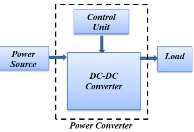
Typically the role of an electrical power converter is to facilitate the transfer of power from source to the load, alongside vice versa, by converting currents and voltages at one specific level to other levels. A DC-DC converter is a power elec-tronic converter that accepts DC input voltages and produce DC output voltages. In the converter, a controller is required to handle power transfer process. Final goal of the complete conversion process is to achieve as closely as possible the required conversion with high performance, and high efficiency (Liu & Lee, 1988). A general DC-DC power converter block diagram is shown in Figure 2.1.
8
Figure 2.1: Block diagram of a DC power converter system (Liu & Lee, 1988).
2.2.2 Basic Circuit of DC–DC Converter
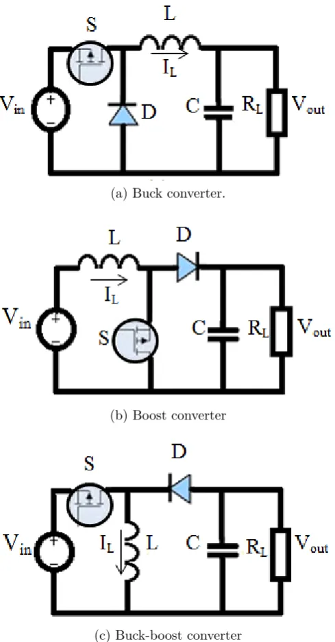
[image:30.595.155.489.68.295.2]9
(a) Buck converter.
(b) Boost converter
(c) Buck-boost converter
Figure 2.2: Basic DC–DC converter topologies (Liu & Lee, 1988).
As shown in Figure 2.2, each of these converters consist of one active power switch S such as for example MOSFET and one passive power switch Dsuch as for example diode. Furthermore the converter circuit offers filter components such as one inductive storage element L, and one capacitive storage component C. Where,Vout is the output voltage, Vin is the input voltage, and RL is the load
The principal function of the buck converter would be to step-down an input voltage to a lower output voltage, i.e.,Vout< Vin. Conversely, the principal
functionality of the boost converter would be to step up an input voltage to an increased output voltage, i.e.,Vout >Vin. The buck-boost converter, because the
[image:31.595.196.441.72.540.2]10
input voltage (Ogata, 1997).
In the basic DC converters, the magnitude of the voltage conversion is directly controlled by the turning-on and the turning-off of the switch. For the buck converter, the power is directly transferred to the output and the capacitive storage when switchSis turned on. This occurs with the energizing procedure for its inductive storage element concurrently. While, for the buck-boost and boost converters, the particular energizing process occurs when switch S is switched-on. The power will be transferred from the inductive storage to the output, and the capacitive storage happens immediately after switch S is switched-off. This indirect power transfers from the source to the load with inductor.
Additionally, in the presence of two switches, these converters could be visualized as a multi-structural system, in which each structure includes a linear circuit construction (Mitchell, 1988). Modification of the circuit configuration is governed by the settings of the switches and the flow from storage currents.
2.2.3 Basic Operation Modes of DC–DC Converter
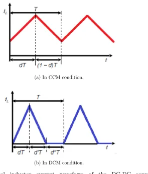
11
(a) In CCM condition.
(b) In DCM condition.
Figure 2.3: Typical inductor current waveform of the DC-DC converters (Mitchell, 1988).
In the CCM operation, the particular turn-on time of the energetic switch S is denoted asdT, where dis the duty ratio and T is the switching time period. Major characteristic of the CCM operation is indicated that the inductor current IL is always more than zero as shown in Figure 2.3(a).
Figure 2.3(b) shows the inductor current waveform when the converter works in DCM. Where, d0T represents time operation when the diode is defi-nitely conducting, and the power switch is open and, d00T represents the time operation when both diode and the switch are open. This time operation could be equivalently indicated as (1−d−d0)T.
2.2.4 Basic Elements of DC-DC Converter
[image:33.595.201.497.74.422.2]par-12
ticular, for a fixed-frequency operation, the dynamic response of the regulation is going to be quicker with smaller values of C orL, since smaller power storage elements need a shorter time to release and store power (Ogata, 1997).
However, a smaller value of L will certainly result in a higher ripple in-ductor current and lower output voltage undershoot or overshoot during a step increment or decrement in load current. Nevertheless, a bigger value of C gives lower output voltage undershoot during a step increment in load current, and lower output voltage overshoot during a step decrement in load current. Each one of these aspects forms dynamic behavior of the converter response.
2.2.5 Basic Switching Frequency of DC-DC Converter
In theory, ideal performance is achievable only when switching frequency is in-finitely high. The term ideal performance means perfect DC steady-state regu-lation, fast dynamic response infinitely, and no overshoot. Nevertheless, since all useful systems are put through time delays and slew rate restrictions in circuit elements, a higher switching frequency procedure is infinitely unattainable.
The particular magnitude of switching frequency is tied to bandwidths of the circuit elements consequently, i.e., the controller, power switch, diode, etc. Additionally, it is known that the amount of power loss in converter rises with the increment of switching frequency. That is true even though soft-switching methods are applied to alleviate the switching losses of the power switches and diodes. Eddy current and current hysteretic losses of magnet elements and resis-tive power losses of the circuit because of skin effect increases with the increment of switching frequency (Ogata, 1997).
By this reason, each one of these losses could be less than the losses gener-ated by the switches relatively. Nonetheless, it must be a consideration whenever determining switching frequency of the converter given that they will become sig-nificant once the frequency is extremely high. Additionally, the emission of higher frequency noise could cause undesirable radio and electromagnetic interferences. Such noise will be the factors that restrict achievable application of extremely fast switching frequency controller to gain an ideal regulation.
Selecting the switching frequency should always be considered a choice of balancing between achieving desired control to meet consumer specifications and reducing power losses, power density, and EMI emission. However, it is true that the performance of the converter can be continually enhanced with an increased switching frequency (Mitchell, 1988).
13
2.2.6 Basic Voltage Regulation of DC-DC Converter
Many DC-DC converters were created with closed-loop feedback controller to pro-vide a regulated output voltage. There are two types of elements in the feedback control scheme, the controlled variable and control gains. The controlled variable is the variable to be controlled (Mitchell, 1988).
In the DC-DC converter, controlled variable is the output voltage and the inductor current. The primary objective, from the perspective of the controller, is to guarantee nullification of the output voltage errors or the inductor current errors for any disturbance, in a well-balanced manner in shortest period. This is carried out through manipulation of controlled variable, by adopting its imme-diate, essential, and/or derivative types because the manipulated variables in its control computation (Tse & Adams, 1990).
The objective of control gains is a multiplication factor to amplify these manipulated variables, so the integrity of the manipulated variables could be intensified. This gives shaping of the controlled behavior in a way that required response can be achieved.
14
Figure 2.4: Equivalent circuit of voltage mode control (Liu & Lee, 1988).
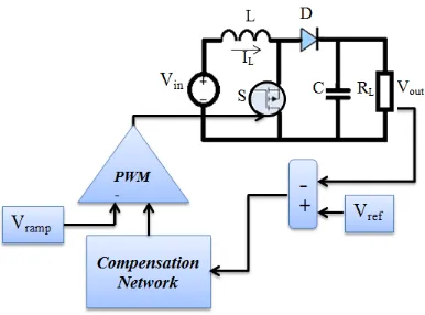
The voltage mode control is a single-loop control where, in fact, the output voltage is regulated by closing a feedback loop between output voltage and duty ratio signal. The output voltage is compared with a constant reference signalVref
to provide voltage errors, which is after that passed through the compensation network to generate a control signal (Mitchell, 1988). The PWM modulator receives compensated control signal to generate the required switching signal for driving power switch. An input voltage feed forwards scheme is required to increase the immunity of converter output voltage against disturbances in input voltage.
2.3 Overview of Multiple-input DC-DC Converter System
[image:36.595.123.509.74.360.2]15
2.3.1 Parallel-Single Input Converters
Figure 2.5 shows the block diagram of an operational system in which convert-ers is connected in parallel. Individual DC-DC convconvert-ersion levels are used for individual sources (Ozpineci et al., 2004; Haque et al., 2006; Di Napoli et al.,
2002; Solero et al., 2005; Lidozzi & Solero, 2004; Amirabadi & Farhangi, 2006;
Camara et al., 2006). These converters are linked together at the DC bus and
controlled independently. In some operational systems, a communication bus could include information and manage power flow between the sources. Various types of such converters are the current-fed push-pull converter, phase-shifted full-bridge converter, three-phase converter, etc. The main drawback of such system is inherently complicated and needs higher cost because of the multiple conversion stages and communication devices between individual converters (Tao
et al., 2006).
[image:37.595.125.528.332.661.2]16
2.3.2 Series-Single Input Converters
A block diagram of series connected converters is shown in Figure 2.6. This configuration is used in low power wind generator and solar panel applications (Chan, 2002, 2007; Chanet al., 1993). In this circuit configuration, output voltage
and current regulation are difficult to be controlled since both tile sources used could have intermittent character (Chan & Chau, 1997; Marwali et al., 2000;
Glavin & Hurley, 2006). The main drawbacks of such systems are that output current flows through both converters and therefore power loss is high (Hirachi
et al., 1995; Sopitpan et al., 2000). Furthermore, gating signals for both input
voltage sources are conjunctive which might create a circulating current in tile two input sources.
Figure 2.6: Series-connected converters (Camara et al., 2006).
2.3.3 Multi-input Converter System
A multi-input DC-DC converter is a converter having more than one energy source as its input. This system results in less components, simple control, more stability, and also reduce losses in the system. Furthermore, the efficiency of power distribution are reinforced dependability at the regulated output voltage (Camara et al., 2006). The basic block diagram of the multi-input converter is
[image:38.595.120.522.297.513.2]17
Figure 2.7: Photovoltaic system using a multi-input converter (Camara et al.,
2006).
2.4 Review of Multi-Input DC-DC Converters
The multiple-input converter is one of the best candidates for renewable energy applications since it can harvest and process power from different sources and energy storages. Multiple-input topology has the advantages of low cost, high power density and ease of management. There have been extensive researches on multiple-input converter in recent years which has resulted in wide spectrum of topologies. Multiple-input converter can be classified into two categories, namely magnetically coupled converter (isolated) and electrically coupled converter (non-isolated).
2.4.1 Previous Works of Isolated Multi-Input DC-DC Converters
In general, isolated multi-input DC–DC converters use leakage inductance as energy storage for transferring power between two sides of the converters. There-fore, the power flow between input and output sides is controlled by adjusting the phase shift angle between primary and secondary voltages of transformer (Camara et al., 2006). According to converter topology, time domain
multiplex-ing, flux addition, and magnetic energy transfer methods are applied in isolated multi-input converters to transfer energy from the primary side of the converter to the secondary (Li et al., 2007).
A general Flyback forward converter based on multiple-input topology to couple energy is shown in Figure 2.8. It was one of the initial versions of isolated multi-input DC–DC converters using time domain multiplexing technique (Zhao
et al., 2011; Kuo et al., 2010; Lin et al., 2009; Chung et al., 2010; Oliveira &
[image:39.595.133.506.72.197.2]18
Figure 2.8: Multi-input flyback DC-DC converter (Zhaoet al., 2008).
Time domain multiplexing in isolated flyback multi-input DC–DC convert-ers is easy to be implemented; however, the energy quantity of such topologies is insufficient due to the nature of Flyback/forward topology. In addition, flyback multi-input converters with winding topology have disadvantages such as, need-ing of a high-value output capacitor, the high current stress in the power switch, high eddy current loss in air-gap area, a large transformer core, and potential EMI problems (Kuo et al., 2010; Lin et al., 2009).
Isolated multi-input DC–DC converters based on flux addition principles with concept of half-bridge isolated converters, full-bridge isolated converters, boost half-bridge isolated converters, and combinational multi-port isolated con-verters as shown in Figure 2.9 and Figure 2.10. Energy from different sources is transferred to secondary by adding total flux in magnetic core from each conver-sion channel (Taoet al., 2008a; Krishnaswami & Mohan, 2009; Wanget al., 2011;
[image:40.595.149.490.73.278.2]19
Figure 2.9: Isolated multi-input boost half-bridge DC-DC converter (Tao et al.,
2008b).
Figure 2.10: Isolated multi-input boost full-bridge converter (Tao et al., 2008b).
Another approach of the multi-input full-bridge converter as shown in Figure 2.11, which based on flux addition of transformer (Chenet al., 2004, 2002).
Two full-bridge cells are coupled together by a transformer with two primary windings and a secondary winding, sharing rectifier diodes and filter capacitor to power the loads (Chen et al., 2001; Matsuoet al., 1998). The full-bridge cells
[image:41.595.112.525.71.252.2] [image:41.595.113.528.326.506.2]20
Figure 2.11: Isolated multiple-input with two full-bridge DC-DC converter (Chen
et al., 2001).
The current-fed multi-input DC-DC converter as shown in Figure 2.12, energy from different power sources can be transferred simultaneously to the load through a multi-winding transformer (Caricchi et al., 1993). But still an issue of
[image:42.595.127.537.79.386.2]21
Figure 2.12: Isolated multiple-input ZVS bidirectional DC-DC converter (Caric-chi et al., 1993).
A high step-up isolated converter with two input sources was investigated, and the converter utilizes the current-source type applying to both of the input power sources is shown in Figure 2.13 (Liu & Li, 2005). To avoid voltage switch-ing spikes caused by the leakage inductor, an active clampswitch-ing circuit is added. However, a large number of power switches are required which cause high cost.
[image:43.595.136.504.64.323.2] [image:43.595.120.520.483.680.2]22
2.4.2 Previous Works of Non-Isolated Multi-Input DC-DC Converters
The power flow control of non-isolated multi-input DC-DC converters is rela-tively straight forward, and their peripheral circuit is usually simple (Marchesoni & Vacca, 2007; Kimet al., 2011). Although non-isolated multi-input DC-DC
con-verters have high flexibility for voltage output, modular structure, and lower cost make non-isolated multi-input converters more favorable in a variety of applica-tions such as renewable energy power station and automotive systems (Spiazzi
et al., 2010; Park et al., 2010; Vazquez et al., 2007).
A general non-isolated multi-input DC-DC converter using H-bridge struc-ture is shown in Figure 2.14 (?Prabhalaet al., 2009). The cascading two H-bridges
with different DC-link voltages, different voltages due to addition or subtraction of H-bridges outputs are accessible.
(a) Buck-buck converter. (b) Buck-buckboost converter.
(c) Buckboost-buckboost converter. (d) Boost-buckboost converter.
[image:44.595.118.535.313.691.2]23
The advantage of these converters is its less number of passive elements, and its disadvantage is an unsuitable control on the power thatis drawn from input sources. Moreover, this converter has high output current ripple due to ripple added from both input voltage sources.
A multi-input DC–DC buck and boost converters are introduced (Liet al.,
2009; Gummi & Ferdowsi, 2010). This converter consists of paralleling two buck converter in their inputs. One switch is series to each input source to prevent short circuit of sources. Figure 2.15 shows a multi-input DC-DC converter with battery/ultra-capacitor for electric vehicle applications.
(a) Boost mode converter.
(b) Buck mode converter.
Figure 2.15: Multiple input DC-DC converter with battery/ultra-capacitor (Li
et al., 2009).
[image:45.595.117.527.253.584.2]24
A multi-input Z-source DC–DC converter is shown in Figure 2.16 (Sedaghati & Babaei, 2011). The structure of proposed converter is changed such that the number of inductors and capacitors is equal to a single input z-source converter. However, two inductors and a capacitor are applied in the proposed converter making the design bulky and costly.
Figure 2.16: Multi-Input Z-Source DC-DC converter (Sedaghati & Babaei, 2011).
A four-phase bidirectional Flyback converter is shown in Figure 2.17 (Bhat-tacharya et al., 2009). In this converter, each of the energy sources can deliver
or absorb energy from the load and other sources. Employment of a separate inductor for each input source is the drawback of this converter.
[image:46.595.171.466.169.342.2] [image:46.595.167.476.465.684.2]References
Ahmadi, R. & Ferdowsi, M. (2012). Double-input converters based on h-bridge cells: derivation, small-signal modeling, and power sharing analysis. Cir-cuits and Systems I: Regular Papers, IEEE Transactions on, 59(4), pp.
875–888.
Ahmadi, R., Yousefpoor, N. & Ferdowsi, M. (2011). Power sharing analysis of double-input converters based on h-bridge cells. In: 2011 IEEE Electric Ship Technologies Symposium.
Ahmadi, R., Zargarzadeh, H. & Ferdowsi, M. (2013). Nonlinear power sharing controller for a double-input h-bridge-based buckboost–buckboost con-verter. Power Electronics, IEEE Transactions on, 28(5), pp. 2402–2414.
Amirabadi, M. & Farhangi, S. (2006). Fuzzy control of a hybrid power source for fuel cell electric vehicle using regenerative braking ultracapacitor. In:
Power Electronics and Motion Control Conference, 2006. EPE-PEMC 2006. 12th International, IEEE, pp. 1389–1394.
Benavides, N.D. & Chapman, P.L. (2005). Power budgeting of a multiple-input buck-boost converter. Power Electronics, IEEE Transactions on, 20(6),
pp. 1303–1309.
Bhattacharya, T., Giri, V.S., Mathew, K. & Umanand, L. (2009). Multiphase bidirectional flyback converter topology for hybrid electric vehicles. In-dustrial Electronics, IEEE Transactions on, 56(1), pp. 78–84.
Bilalovic, F., Music, O. & Sabanovic, A. (1983). Buck converter regulator op-erating in the sliding mode. Proceedings VII International PCI, 10, pp.
333–340.
Camara, M., Gualous, H., Gustin, F. & Berthon, A. (2006). Control strategy of hybrid sources for transport applications using supercapacitors and batter-ies. In: Power Electronics and Motion Control Conference, 2006. IPEMC 2006. CES/IEEE 5th International, volume 1, IEEE, pp. 1–5.
158
Cao, J. & Emadi, A. (2012). A new battery/ultracapacitor hybrid energy stor-age system for electric, hybrid, and plug-in hybrid electric vehicles. IEEE Transactions on Power Electronics,, 27(1), pp. 122–132.
Caricchi, F., Crescimbini, F., Capponi, F.G. & Solero, L. (1998). Study of bi-directional buck-boost converter topologies for application in electrical vehicle motor drives. In: Applied Power Electronics Conference and Expo-sition, 1998. APEC’98. Conference Proceedings 1998., Thirteenth Annual,
volume 1, IEEE, pp. 287–293.
Caricchi, F., Crescimbini, F., Napoli, A., Honorati, O. & Santini, E. (1993). Testing of a new dc/dc converter topology for integrated wind-photovoltaic generating systems. In: Power Electronics and Applications, 1993., Fifth European Conference on, IET, pp. 83–88.
Chan, B.C. (2007). The state of the art of electric, hybrid, and fuel cell vehicles.
Proceedings of the IEEE, 95(4), pp. 704–718.
Chan, C. (2002). The state of the art of electric and hybrid vehicles. Proceedings of the IEEE, 90(2), pp. 247–275.
Chan, C. & Chau, K. (1997). An overview of power electronics in electric vehicles.
Industrial Electronics, IEEE Transactions on, 44(1), pp. 3–13.
Chan, H.C., Chau, K. & Chan, C. (1993). A neural network controller for switch-ing power converters. In: Power Electronics Specialists Conference, 1993. PESC’93 Record., 24th Annual IEEE, IEEE, pp. 887–892.
Chandrakar, Y. (2013). Comparison of open loop and closed loop models for dual input dc-dc boost converter.International Journal of Emerging Technology and Advanced Engineering.
Chen, Y.M., Liu, Y.C., Wu, F.Y. & Wu, T.F. (2001). Multi-input dc/dc converter based on the flux additivity. In: Industry Applications Conference, 2001. Thirty-Sixth IAS Annual Meeting. Conference Record of the 2001 IEEE,
volume 3, IEEE, pp. 1866–1873.
Chen, Y.M., Liu, Y.C. & Lin, S.H. (2006). Double-input pwm dc/dc converter for high-/low-voltage sources. Industrial Electronics, IEEE Transactions on, 53(5), pp. 1538–1545.
159
Chen, Y.M., Liu, Y.C. & Wu, F.Y. (2004). Multiinput converter with power factor correction, maximum power point tracking, and ripple-free input currents. Power Electronics, IEEE Transactions on, 19(3), pp. 631–639.
Chung, S.K., Lim, J.G. & Song, Y. (2010). Active clamped three-phase isolated boost converter with series output connection for high step-up applica-tions. In: Energy Conversion Congress and Exposition (ECCE), 2010 IEEE, IEEE, pp. 1090–1097.
Danyali, S., Hosseini, S.H. & Gharehpetian, G.B. (2014). New extendable single-stage multi-input dc–dc/ac boost converter. Power Electronics, IEEE Transactions on, 29(2), pp. 775–788.
De Doncker, R.W., Divan, D.M. & Kheraluwala, M.H. (1991). A three-phase soft-switched high-power-density dc/dc converter for high-power applications.
Industry Applications, IEEE Transactions on, 27(1), pp. 63–73.
Dhivya, B., Krishnan, V. & Ramaprabha, R. (2013). Neural network controller for boost converter. In: Circuits, Power and Computing Technologies (IC-CPCT), 2013 International Conference on, IEEE, pp. 246–251.
Di Napoli, A., Crescimbini, F. & Solero, L. (2002). Control strategy for multiple input dc-dc power converters devoted to hybrid vehicle propulsion systems. In: Industrial Electronics, 2002. ISIE 2002. Proceedings of the 2002 IEEE International Symposium on, volume 3, IEEE, pp. 1036–1041.
Ding, G. & Kwasinski, A. (2013). Digital constant on-time controlled multiple-input buck and buck-boost converters. In: Applied Power Electronics Con-ference and Exposition (APEC), 2013 Twenty-Eighth Annual IEEE, IEEE,
pp. 1376–1382.
Duarte, J.L., Hendrix, M. & Simões, M.G. (2007). Three-port bidirectional con-verter for hybrid fuel cell systems. Power Electronics, IEEE Transactions on, 22(2), pp. 480–487.
El Fadil, H., Giri, F., Haloua, M. & Ouadi, H. (2003). Nonlinear and adaptive control of buck power converters. In: Decision and Control, 2003. Pro-ceedings. 42nd IEEE Conference on, volume 5, IEEE, pp. 4475–4480.
Fa-Qiang, W., Hao, Z. & Xi-Kui, M. (2008). Studied on low-frequency oscillation in the boost converter with one cycle control.
160
In: Recent Advances and Innovations in Engineering (ICRAIE), 2014,
IEEE, pp. 1–6.
Glavin, M. & Hurley, W. (2006). Battery management system for solar en-ergy applications. In: Universities Power Engineering Conference, 2006. UPEC’06. Proceedings of the 41st International, volume 1, IEEE, pp. 79–
83.
Govindaraj, D.T. & Abraham, S.S. (2014). Modified time sharing switching tech-nique for multiple input dc-dc converter fed pmdc drive. Innovative Re-search In Electrical, Electronics, Instrumentation And Control Engineer-ing, 2(1).
Guldemir, H. (2011). Study of sliding mode control of dc-dc buck converter.
Energy and Power Engineering, 3(04), p. 401.
Gummi, K. & Ferdowsi, M. (2010). Double-input dc–dc power electronic convert-ers for electric-drive vehicles - topology exploration and synthesis using a single-pole triple-throw switch. industrial Electronics, IEEE Transactions on, 57(2), pp. 617–623.
Haque, R.U., Iqbal, M.T. & Quaicoe, J.E. (2006). Sizing, dynamic modeling and power electronics of a hybrid energy system. In: Electrical and Computer Engineering, 2006. CCECE’06. Canadian Conference on, IEEE, pp. 1135–
1138.
Hirachi, K., Yamanaka, M., Takada, T., Mii, T. & Nakaoka, M. (1995). Feasible developments of utility-interactive multi-functional bidirectional converter for solar photovoltaic generating system incorporating storage batteries. In: Power Electronics Specialists Conference, 1995. PESC’95 Record., 26th Annual IEEE, volume 1, IEEE, pp. 536–541.
Ilka, R Gholamian, S.A.R.B. & Rezaie, A. (2012). Fuzzy control design for a dc-dc buck converter based on recursive least square algorithm.International Journal on Computational Sciences & Applications, 2(6), pp. 9–12.
Ismail, N.N., Musirin, I., Baharom, R. & Johari, D. (2010). Fuzzy logic controller on dc/dc boost converter. In: Power and Energy (PECon), 2010 IEEE International Conference on, IEEE, pp. 661–666.
Jeong, G.J., Kim, I.H. & Son, Y.I. (2009). Application of simple adaptive control to a dc/dc boost converter with load variation. In: ICCAS-SICE, 2009,
161
Jiang, W. & Fahimi, B. (2011). Multiport power electronic interface - concept, modeling, and design. Power Electronics, IEEE Transactions on, 26(7),
pp. 1890–1900.
Khaligh, A., Cao, J. & Lee, Y.J. (2009). A multiple-input dc–dc converter topol-ogy. Power Electronics, IEEE Transactions on, 24(3), pp. 862–868.
Kim, K.D., Kim, J.G., Jung, Y.C. & Won, C.Y. (2011). Improved non-isolated high voltage gain boost converter using coupled inductors. In: Electri-cal Machines and Systems (ICEMS), 2011 International Conference on,
IEEE, pp. 1–6.
Krishnaswami, H. & Mohan, N. (2009). Three-port series-resonant dc–dc con-verter to interface renewable energy sources with bidirectional load and energy storage ports. Power Electronics, IEEE Transactions on, 24(10),
pp. 2289–2297.
Kumar, L. & Jain, S. (2013). Multiple-input dc/dc converter topology for hybrid energy system. IET Power Electronics, 6(8), pp. 1483–1501.
Kumar, S. & Ikkurti, H. (2011). Design and control of novel power electronics interface for battery-ultracapacitor hybrid energy storage system.
Kuo, P., Liang, T., Tseng, K., Chen, J. & Chen, S. (2010). An isolated high step-up forward/flyback active-clamp converter with output voltage lift. In:
Energy Conversion Congress and Exposition (ECCE), 2010 IEEE, IEEE,
pp. 542–548.
Kwasinski, A. (2009). Identification of feasible topologies for multiple-input dc–dc converters.Power Electronics, IEEE Transactions on, 24(3), pp. 856–861.
Leyva, R., Martinez-Salamero, L., Jammes, B., Marpinard, J.C. & Guinjoan, F. (1997). Identification and control of power converters by means of neural networks. Circuits and Systems I: Fundamental Theory and Applications, IEEE Transactions on, 44(8), pp. 735–742.
Li, W., Liu, J., Wu, J. & He, X. (2007). Design and analysis of isolated zvt boost converters for high-efficiency and high-step-up applications. Power Electronics, IEEE Transactions on, 22(6), pp. 2363–2374.
Li, Y., Yang, D. & Ruan, X. (2008). Interleaved dual-edge modulation scheme for double-input converter to minimize inductor current ripple. In: Power Electronics Specialists Conference, 2008. PESC 2008. IEEE, IEEE, pp.
162
Li, Z., Onar, O., Khaligh, A. & Schaltz, E. (2009). Design and control of a multiple input dc/dc converter for battery/ultra-capacitor based electric vehicle power system. In: Applied Power Electronics Conference and Exposition, 2009. APEC 2009. Twenty-Fourth Annual IEEE, IEEE, pp. 591–596.
Lidozzi, A. & Solero, L. (2004). Power balance control of multiple-input dc-dc power converter for hybrid vehicles. In: Industrial Electronics, 2004 IEEE International Symposium on, volume 2, IEEE, pp. 1467–1472.
Lin, B.R., Dong, J.Y. & Chen, J.J. (2009). Active-clamp zvs converter with step-up voltage conversion ratio. International Journal of Electronics, 96(5),
pp. 491–502.
Liu, D. & Li, H. (2005). A novel multiple-input zvs bidirectional dc-dc converter. In: Industrial Electronics Society, 2005. IECON 2005. 31st Annual Con-ference of IEEE, IEEE, pp. 6–pp.
Liu, F., Wang, Z., Mao, Y. & Ruan, X. (2014). Asymmetrical half-bridge double-input dc/dc converters adopting pulsating voltage source cells for low power applications. Power Electronics, IEEE Transactions on, 29(9), pp.
4741–4751.
Liu, K.H. & Lee, F.C. (1988). Topological constraints on basic pwm converters. In: IEEE PESC, volume 88, pp. 64–172.
Marchesoni, M. & Vacca, C. (2007). New dc–dc converter for energy storage system interfacing in fuel cell hybrid electric vehicles. Power Electronics, IEEE Transactions on, 22(1), pp. 301–308.
Marwali, M., Maricar, N. & Shrestha, S. (2000). Battery capacity tests evalua-tion for stand-alone photovoltaic systems. In: Power Engineering Society Winter Meeting, 2000. IEEE, volume 1, IEEE, pp. 540–545.
Matsuo, H., Lin, W., Kurokawa, F., Shigemizu, T. & Watanabe, N. (2004). Characteristics of the multiple-input dc-dc converter. IEEE Transactions on Industrial Electronics, 51(3), pp. 625–631.
Matsuo, H., Kobayashi, K., Sekine, Y., Asano, M. & Wenzhon, L. (1998). Novel solar cell power supply system using the multiple-input dc-dc converter. In: Telecommunications Energy Conference, 1998. INTELEC. Twentieth International, IEEE, pp. 797–802.