+-~~---~---.--~---~-.---
I/
HEW LET T PAC K A R D C O. /
I IOERS
hp /
/
~---~---~---~-.---.-+
...
-Ltr Revisions Date Appr'd
A As Issued : 12/20/821 DH
: MODEL :STK /I
;_.+ _________ + __ M~ _ _ _ +-~.~-~~--+----~~-~-~---
__
.~_+---_____ ._. _____
~--.--_~___ _
I I
I 1/0 System ERS
1 BY Fred Gross :DATE 09/20/82
;-.+---+---..
ILTI P.C. II APPR+----.----+---~~-.~-.---~.---+---~--~:
DATE IAPPD ~SHEET /I 1 OF 80...
-+-.---.--- /
/
lOERSI hp I
HEW LET T - PAC K A R D C O. I I
---._---+
---TABLE OF CONTENTS
Page
1 INTRODUCTION 4
1 • 1 OVERVIEW 4
1.2 LIST OF 1/0 STATE INFORMATION 5
2 lOP OPERATION 6
2.1 SYSTEM COMMUNICATION 6
2.2 INTERFACE POLLING 6
2.3 DIRECT I/O OPERATION 9
2.4 DIRECT MEMORY ACCESS 9
2.5 INTERRUPT REQUESTS 10
2.6 1/0 BUS 12
2.6. 1 Functional Description 12
2.6.2 Electrical Specifications 14
3 DIRECT MEMORY TRANSFER 16
3. 1 DMA TRANSFERS 16
3. 1 • 1 DMA Single Transfer per Poll Response 17
3. 1 .2 DMA Multiple Transfers per Poll Response 18
3. 1 .3 Request to Access Memory - Direct 18
3.2 DMA OPTIONS 18
3.2.1 DMA Verify 19
3.2.2 DMA Match 19
4 INTERRUPT REQUESTS 20
4. 1 CPU SERVICE 20
4 • 1 • 1 Interrupt Request Register 20
4. 1 .2 Interrupt Mask Register 20
4. 1 .3 Mapping PA to Interrupt Level 20
4.1.4 Recording CPU Interrupt Requests 21
4.2 CPU OPERATIONS 24
4.2.1 Interrupt ~asking 24
4.2.2 Identifying the Interrupting Device 24
4.2.3 Reaching the Service Routine 25
4.2.4 Interrupt Routine Exit 26
4.3 MPB COMMAND EXECUTION BY lOP 27
4.4 ATTENTION REQUESTS 27
5 MPB
lID
COMMANDS 295. 1 DMA COMMANDS 29
5.2 INTERRUPT COMMANDS 32
5.3 INTERVAL TIMER COMMANDS 33
lMODEL lSTK /I
:~~+~.~---+----~--+-~---+-~--.--~-.--~~~---+-.---.---.-
...
---~.~--.I
: lID
System ERSI
l--+---+---+---+---+---lBY Fred Gross lDATE 09/20/82
lLT: P.C. H : APPR DATE \APPD ISHEET H 2 OF 80
---+---~--.--~---~---~---.-~
..
~.~--
/ /
lOERSI
I hp I
HEW LET T - PAC K A R D C O. I I
---+
5.4 DIRECT 1/0 COMMANDS
5.5 OTHER COMMANDS
5.6 INSTRUCTIONS FOR COMMAND EXECUTION ONLY
34 35 39
6 CPU INSTRUCTION FOR 1/0 43
6.1 1/0 INSTRUCTION FORMAT 43
6.2 1/0 INSTRUCTION PARAMETERS 43
1 INTERVAL TIMER 45
1.1 TIMER UNDERFLOW 45
1.2 TIMER ACCURACY AND PRECISION 45
8 INITIALIZATION 46
8.1 POWER ON 46
8.2 RESET 46
8.3 SELF TEST GENERAL DESCRIPTION 41
8.4 SELF TEST OBJECTIVES 48
8.5 INDIVIDUAL MODULE DESCRIPTION 50
9 HARDWARE DESCRIPTION 53
9.1 REGISTERS AND SPECIAL FUNCTIONS 53
9.1.1 Interrupt 53
9.1.2 Micro-Control Registers 56
9.1.3 1/0 Bus Registers 56
9.1.4 Interval Timer Registers 56
9.1.5 Other Registers and Functions 51
9.2 DMA REGISTERS 58
9.2.1 DMA Active Registers 58
9.2.2 DMA Logical Registers 59
9.3 MICROPROGRAM SEQUENCING AND SUPPORT HARDWARE 60
9.3.1 Addressing Control Store 60
9.3.2 Microaddress Registers and Incrementers 60
9.3.3 Special Sequencing 61
9.3.4 Microcoding lOP with Pipelined Microcode 61
9.4 PLA MICROINSTRUCTION DECODER 61
9.5 ROM CONTROL STORE 61
Appendix 63
Timing Diagrams
:MODEL ISTK #
: 1/0 System ERS
-+---+---+---+---+---
: : : IBY Fred Gross :DATE 09/20/821--+---+---+---+---+---ILTI P.C. # I APPR : DATE IAPPD :SHEET # 3 OF 80
---+-.~~---
..
---.--.-~~-~.-.---.
/ /
IOERS HEW LET T - PAC K A R D1 INTRODUCTION
1.1 OVERVIEW
C O.
/ hp /
/ / ---..
---.-~~~---~~--~.-+---The input/output channel for the FOCUS System is the lOP
(Input/Output Processor). The lOP is a valid implementation
of a subset of a CSG Channel Adapter. The lOP will support
all CSG Device Adapters. The mechanisms of I/O include direct
I/O by the CPU, CPU interrupts, MPB Command execution by lOP,
and direct memory accesses (DMA) by the lOP. A FOCUS system
may contain up to six lOP's, each having an addressing capability for eight interfaces.
The lOP is controlled by commands sent over the MPB
(Memory-Processor Bus) from the main CPU or a CPU dedicated to
I/O and/or other special tasks. Data transfers independent of
the CPU are controlled by eight DMA resources in the lOP.
The lOP external I/O bus is a synchronous bus capable of 8
or 16 bit transfers with separate address and bidirectional
data lines.
A periodic interface poll is used for detecting interface
service and data requests. An affirmative response to the
poll will be interpreted as a data request if the poll winning
interface has its DMA mask bit set. Checking status will
determine if the request was for a DMA transfer or an interrupt since a DMA transfer request will only occur if status is true.
By loading the lOP registers with the appropriate information and starting DMA, data can be transferred
independent of the CPU. Data will be transferred by bytes or
by half-words until a count has been exhausted, a status error is detected, Device End is asserted, or optionally a character
(byte mode only) match is detected. An interrupt request will
be recorded at the end of a DMA operation or at an error condition.
MPB Command chaining is possible by setting a bit in the
Status register. A list of write or control
MPB
Commands willbe executed by the lOP one per poll cycle if no DMA is
requested. The fourth word of the DRT points to the list. If
the Status register bit is not set, normal interrupts occur.
1--+---+---+---+---+---
I I I II t I I IMODEL :STK #
l--+---+---+---+---+---I l I/O System ERS
,
1--+---+---+---+---+---,
IBY Fred Gross IDATE 09/20/82
;LT; P.C. # ; APPR ~ DATE :APPD :SHEET
n
4 OF 80 :---+ •• --- •• - - - . - - - - . - . - - - - . - - - - I I IOERS
I
I hp I
HEW LET T - PAC K A R D C O. I I
---.---+
Interrupt requests for each interface can be masked
individually on the lOP and all CPU interrupt requests from an
lOP can be masked on the CPU. There are sixteen
interface-address-independent levels of interrupt. Any number of
interfaces may be assigned to a priority level.
1.2 LIST OF 1/0 STATE INFORMATION
The bit numbering convention used in this ERS is consistent with the CPU ERS in that the most significant bit is to the
left and it is the lowest numbered. The
IIO
bus, however, i~numbered with the MSB to the left and it is the highest numbered.
Previous interfaces refered to addressable registers as R4
through R7 corresponding to IC addresses 0000 to 0011. All
future references will be FRO thru FR15 corresponding to IC address 0000 to 1111.
A FOCUS system may contain up to six lOP's, each with an
interface addressing capability of eight. Every interface has
a four word entry in the system's memory-resident Device
Reference Table (DRT). The address of the first word of a DRT
entry is computed as follows:
OOC CCP PPO 000 (byte address)
Where CCC is the Channel Number of the lOP and PPP is the
Peripheral Address of the Interface. The first channel is
number 1. Each device entry has four words which contain the
following information:
Link I Operating System Information
Data Segment Pointer
Interrupt Service Routine Pointer MPB Command List Pointer
The first word contains link information for interrupts and
operating system information. The second word contains a data
segment pointer which points to the global data segment used
by the interrupt service routine. The third word contains a
program pointer which points to the interrupt service routine
for the device. The fourth word contains the MPB Command List
Pointer.
IMODEL ISTK #
--+-~~-~----+~-~-.--+~---.+~--~---~.~-~.~~--~+---··-~--···---··---~---I
I
I
I
1/0 System ERS
:BY Fred Gross IDATE 09/20/82
---+-~-~---~----~---~---~---.--
/ /
lOERS.I hp I
HEW LET T - PAC K A R D C O. I I
---+
lOP OPERATION
2.1 SYSTEM COMMUNICATION
Communication between lOP's and CPU's or memory is done
over the Memory Processor Bus (MPB). (For a detailed
description of the MPB and its protocol see the Memory
Controller ERS.) A channel number is assigned to each lOP
from the range 1 to
7.
The lOP uses byte, half-word, and word transactions with memory on the Y channel and word transactions on the X
channel. In addition to reads and writes the lOP will also
use semaphore operations with memory. The lOP will receive
message bits from memory to indicate double bit memory errorst
slave address errors, slave data errors, and slave write data valid.
The lOP communicates with CPU's by receiving channel-to-channel communications (MPB commands) and it can write to a CPU using channel-to-channel communication in response to a
request for data. It can respond to an 1/0 device's need for
service by sending the CPU a channel message (an interrupt). The channel message may be a broadcast message if no specific CPU channel address is stored on the lOP.
System Interrupts (Sys. Int. in Fig. 2.1) refer to message
bits 0-2 and 6-15. Defined bits that lOP recognizes are: 0
for double bit m~mory errors, 1 for slave address error, 2 for
slave data error. The lOP sends the following messages:
7
forillegal MPB Command, 8 for MPB error, 9 for double bit memory error, 13 for timer interrupt, 14 for CSG attention requests,
16-31 for 1/0 interrupts.
2.2 INTERFACE POLLING
Interfacing polling is the background activity for the 1/0
bus (See Figure 2.1). A poll occurs when the lOP sets INT
true and latches the IOD lines some time later. An interface
requesting service will set an laD line corresponding to its
PA true. Whenever an 1/0 operation is completed, interface
polling is begun to allow interfaces to request service.
Because responding interfaces may be requesting either a DMA data transfer or an lOP MPB command or a CPU interrupt, those
...
+ ... - ... I I IOERS
I hp I
HEW LET T .. PAC K A R D C O. I I _ .. _ ... _ ... +
...
interfaces enabled to do DMA and enabled given a DMA transfer unless the STS line If more than one interface enabled to do responds, then the highest PA responding receive service first.
for interrupt are is asserted false. DMA or interrupt interface will
: ... + ... + ... + ... + ... + ... - .. ..
I I I I
I t t I :MODEL lSTK II
:-.+--~~-~-~~+-~---+--~.-.---+---
..
--~~---+.----.----.~--~~.---.~~---I l 1/0 System ERS
: BY Fred Gross :DATE 09/20/82
l ... + ... ... + ... + .. ... .. + ... .... .... · ... + ... .... ... .. ..
-ILTI P.C. /I APPR DATE IAPPD ISHEET /I 7 OF 80
/
1 tit .. 1
:.
t T ;.i c [)
c
D. 1 1---+
I
f\6-2.f
--t---+---~---+---+---~---I I t MODEL I STK #
--.---+---+---+---+---!
I/U System ERS
--~---+---+---
+---IBY rre0 Gross IDATE 09/20/82
---+---+---+---+---1
U . I ( - , I p. P ~) R I D ' ; T E I~. ? P D I S H r.~ E T F 8 u F H 1 I
--t---+---+---+---+---1
K t \I (S If) I!.s I S LJ P t: r< S~: U r~ SID:~ G 11 A - 1 F Pol - 3030 - 9 I
---+ __ •• ___ M _ _ _ _ ~ _ _ _ _ _ • _ _ _ _ _ _ _ _ _ _ _ • _ _ _ _ _ _ _ _ _ _ ~~ / / lOERS
/ hp /
HEW LET T - PAC K A R D C O. I /
---+
2.3 DIRECT I/O
I
Direct I/O by a CPU is performed when the CPU encounters an I/O instruction and translates that instruction into MPB
commands. The MPB command is sent to the lOP's slave address
register, with data sent to the slave data register. Contained in the information sent to the slave address
register will be lOP destination, the peripheral address of the interface, the operation to be performed, and, if the instruction was a read, the CPU's return address.
Before a transfer takes place, it is necessary for the 1/0
driver to check status and flag to insure the interface will be able to receive or send data when the bus is strobed. Reading from an interface instructs the lOP to send a data
word to the CPU when the
lID
read operation is complete.2.4 DIRECT MEMORY ACCESS
As shown in Figure 2.2, the interface poll response, IOD
0-7, is AND'ed with the DMA Mask register to determine whether a
request by an interface enabled to do DMA exists. If so, the
highest priority interface is addressed and responds with
STATUS. If true a DMA data transfer is done to the interface
and if burst DMA (multiple transfers per poll response) is
requested, an entire burst is done. If STATUS is false, the
DMA transfer to that interface is terminated. Termination of
DMA for any reason (other than by CPU) causes a bit in the Interrupt Request register to be set to indicate an interrupt request from the appropriate PA.
If no interface requests service by poll response, the RAMD
line is checked for a valid response. If a true response
exists and if RAMD is enabled (MSB of DMAPA
=
1) then the PAin the DMAPA register will be enabled for a data transfer. A
single data transfer or multiple transfers can take place when
RAMD is true. All RAMD transfers are done through FR8 or
FR10. The intended use of this line is to allow compatibility
with Greyhound and it should NOT be used in future interface designs.
:--+---+---+---+---+---;
: : I : :MODEL :STK # :
:-~+~~---~+.---+---~--+----~--.---+--~~---~~~.--~~----~~-;
! : : : 1/0 System ERS
-+---+---+---+---+---:
I I I IBY Fred Gross IDATE 09/20/82 :,
1--+---+---+---+---+---1
ILTI P.C. # : APPR DATE IAPPD ISHEET # 9 OF 80 I+---.---..
---.--.----~---.----~---~-
/
/
lOERSI hp I
HEW LET T - PAC K A R D C O. / / ---+
7
o
IPriorityl +---+---IInterface Poll:
Encode I---Iandl +---+
+---+
I
I
Service Request
+---+
I
,
DMA request
24 31
+---+
I +---+---IInterrupt Mask:
+-lor +---+
+---+--+
24 31
+---+ DMA Mask
Figure 2.2 Valid Interrupt Request
2.5 INTERRUPT REQUESTS
Valid interrupt requests are either sent to the CPU or processed by MPB command list by the lOP, depending on a bit
in each PA's status register. The highest responding PA may
request either OMA or interrupt and be given service.
Interrupt requests result from four kinds of events: a
response to the interface poll on the 1/0 bus, termination of
a DMA block transfer, setting the interrupt request bit by MPB command, and events not related to one of the eight PA's.
These latter events include the interval timer interrupt , memory errors on accesses by the lOP, and attention request interrupts and they are always sent to the CPU as interrupts.
CPU interrupt requests, except from memory errors or from
--+---+---+---+---+---:
I : IMODEL lSTK # :
--+---+---+---+---+---:
: I : 1/0 System ERS
-+---+---+---+---+---:
: : I lBY Fred Gross IDATE 09/20/82 :
1--+---+---+---+---+---1
ILT: P.C. # I APPR : DATE IAPPD ISHEET # 10 OF 80 :
1--+---+---+---+---+---~
[image:10.613.68.520.44.471.2]+--~--.----.---~-.---~.---
I/
hp I/
IOERSHEW LET T - PAC K A R D C O. I I
---+
---the timer, can be masked individually on ---the lOP or all
IIO
interrupts can be disabled at the CPU. In addition to this,
each PA on each channel is assigned an interrupt priority
level, 0-15, which is determined by software and stored on the
lOP. The CPU automatically masks interrupt requests whose
levels are equal to or less than the level of the interrupt
service routine that the CPU is executing. This creates
sixteen level interrupt structure with additional masking of
individual devices and the option of operating with
IIO
interrupts disabled.
Interrupt requests serviced by the lOP are handled by
executing one MPB command per poll when there is no valid DMA request and when a bit in the status register requests MPB command execution by lOP.
:--+---+---+---+---+---l
: : : MODEL :STK # : :-~+-~-~-~~.~+---~-+----~--~.+-~---~~---.~~+~---.-.-~~-~-~.-~---~~~-~~--,I liD System ERS :
-+---+---+---+---+---1
: : : lBY Fred Gross IDATE 09/20/82 :I
l--+---+---+---+---+---1
ILTI P.G. # l APPR l DATE lAPPD :SHEET # 11 OF 80 :1--+---+---+---+---+---1
I+~--~--.---.----.~---~---
I/ /
hp I IOERSHEW LET T - PAC K A R D C O. I I
---+
~. 6 1/0 BUS
2.6.1 Functional Description of 1/0 Bus Lines
lOP provides an 1/0 bus which has features compatible with
980XX interface cards and with the CSG 10 cards. Interrupt
lines (IRH, IRL) have been eliminated in favor of doing an
interface poll periodically. Immediately after power on,
POUT, NDOUT, NRESET, NIOSB, and NINT are initialized active.
The 1/0 bus has the following lines:
No. 16 3 1 1 1 1 1 1 1 1 1 1 1 1 CSG DB[15:0] PA[2:0] BP[1] CBYT CEND SP[D] IOSB POLL DOUT SR IFC ARQ DEND Old
01015 ... 0 PA2-0 IC4 IC3 IC2 ICl FLG STS IOSB INT DOUT BR RESET ASYNC(WAIT) RAMD Description
Data Lines
Peripheral Address
Bus Primitivel Interface Control
Channel Byte Channel End
Bus Primitivel Interface Control
Interface Flag Interface Status
1/0 Strobe
Interface Poll
Data Direction (true=out of lOP)
DMA Burst Request Interface Clear/Reset Attention Requestl Asynchronous Handshake Device Endl Request for Accessing Memory Direct
The sixteen bidirectional data lines are used for
transferrin:
e
or 16 bit quantities in either direction. Theyare also used by interfaces to respond to a poll.
The three peripheral address lines are used to select one
of eight interfaces. When an interface recognizes its
address, it immediately asserts status and flag.
The four interface control lines are used to inform the interface about the destination or source of data on the next
:--+-_ .... _-_._+---_ ... +---_.+---_._---+ ... _---_ ... ---
I I I I' I I I : MODEL :STK /I
:--+---+---+---+---+---
I I I I. I I I
I
lID
System ERS.+----_ ... _--+--_ ... _--+ .... __ ._---+----_._---+---... _-:
I : : : IBY Fred Gross :DATE 09/20/82 :
:--+---+---+---+---+---1
ILTI P.C. /I I APPR DATE IAPPD ISHEETU
12 OF 30:--+---+---+---+---+---:
---+~~~-~~~~.--.----~~~~-~---.---~~
/ /
IOERSI
J
~
I hp I
HEW LET T - PAC K A R D C O. I I
---+
strobe.
The Flag line exists for compatiblity and is used only
during MPB Command to read flag. A true response on the flag
line is the interface's assurance that it will allow access to the addressed register on the next strobe.
The Status line is used to signal the lOP that an
exceptional status condition exists on the interface (STS =
Card Address
*
Card in Slot*
Not Exceptional Status). Statusmust be true for a DMA data transfer and any status false
after a request for service will result in DMA termination and an interrupt request bit set.
The trailing edge of 1/0 Strobe can be used by an interface
to latch data on a data out cycle. During burst input, the
trailing edge of strobe indicates the next data may be placed on the data lines.
The Interface Poll line is asserted by lOP between 1/0 bus
cycles. The purpose of this line is to check the interfaces
for service requests which may result in an interrupt request
or a DMA data cycle. An interface responds by driving the
data line corresponding to its PA. An interface must not
change its response (either a request or non-request) during a
poll cycle. IC4 (BP[1]) determines if the poll is a Service
Request poll (IC4=0) or an Attention Request poll. IC1
(BP[O]) is zero during a Service Request poll.
The Data Direction line determines the direction of data transfer and is used by the interface to know when to drive the data lines.
The DMA Burst Request line is used to request a DMA burst
during a DMA transfer. Bursts are terminated when Burst
Request goes false or when 32 transfers take place, whichever
occurs first. The length of 1/0 Strobe is shortened during a
burst transfer. The assertion of Burst Request implies a
valid status condition.
The Reset line is used to initialize the interfaces to a
known state (Interface Clear). The line can be asserted by
MPB Command.
The Async (Wait) line allows an interface to extend the
IMODEL :STK
n
I~-+---·+--~----+-~---·+~--·-~---~-·-~-+---~---~.-.---~~~~-
I : 1/0 System ERS
-+---+---+---+---+---:
: I I lBY Fred Gross :DATE 09/20/82 :,
:--+---+---+---+---+---1
ILT~ P.C.n :
APPR I DATE lAPPD . lSHEETn
13 OF 80 :...
+.--~--~-~~.-~~~-.-.~.---~---~~~~~~-.-~~--
/ /
IOERSI hp I
HEW LET T .. PAC K A R D C O. I I .... - ... _ ... _ ... - .... +
...
-length of 1/0 strobe. Async is ignored when Burst Request is
true. The extension is eight states. Async is also used
during poll cycles as a request for an Attention Poll (See Attention Request).
The Request to Access Memory .. Direct line is used to
request a DMA transfer without responding to a poll. The line
is tested for a valid response at the end of checking for a
valid DMA poll response. Only one interface should be enabled
to respond on this line and that interface's PA is stored in
the DMAPA register. This line is also used as Device End (See
CSG 1/0 Standards) in a time multiplexed way. During an
Interface Poll t the line is used to detect RAMD requests.
When Interface Poll is false, the line is used to detect Device End (except when RAMD burst transfers are taking place) •
The POUT line controls the direction of the external
buffers. It also enables the laD lines from the lOP
internally. This line is positive true.
The line DB5 is used to turn the self test LED on and off.
It also controls the enable for the input buffers. If DB5 is
high, the LED is on and the inputs to lOP are disabled.
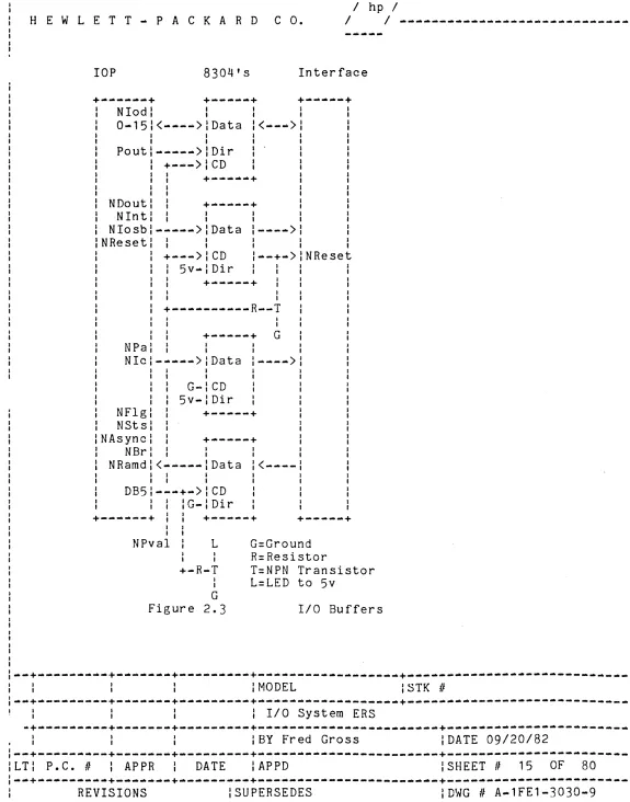
~.6.2 Electrical Specifications
The 1/0 Bus lines have negative true logic. This means a
low voltage is an active signal and a high voltage is an
inactive signal. The one exception to this is the POUT
control line which is positive true logic.
The recommended external buffers are the 8304B
Bidirectional Transceivers. They are fast enough to allow a
four state burst mode at 18 MHz and provide ~OS logic levels
(3.6 v. min.) required by the rap. Figure 2.3 shows the lOP
to external buffer interface.
-~+-.----~-~+~-~---~+~---~+-.-~---~---+.-.~---~---.--.--~~~~~~--:
: : : lMODEL :STK
n
t--+~~~~~-~-~+~~~~---+~-·~-~-~-+-~---~~-~~--~-~-~~+---~~--~-~-~-~-~.~~~~~~~-~--;
I : 1/0 System ERS
-+---.... -+ .. -.... -.... +-... -+ ... --.... ---... ---+---.. ----... ---l
I I II I I : BY Fred Gross IDATE 09/20/82
ILTI P.C.
n :
APPR DATE IAPPD ISHEET # 14 OF 80+~-.~-~~~~---~~~~.~-~-~~~--~~~--~~-~~--~--~~
/
I hp I
HEW LET T PAC K A R DCa. I I
ILT: P.C. II
lOP 8304's Interface
+---+ +---+ +---+
I Nlod:
I I I I
0-151<---->IData 1<--->1 :
I I
, I
Poutl--->IDir : +--->ICD
I
,
I,
I I I
,
,
I I
,
I
,
NDout: +---+
Nlnt: I I :
I Nloshl--->IData 1---->
INResetl I I
+--->ICD 1--+->INReset
I 5v-IDir
+ ... - ... ~ .... R ... T
NPa Nlc
1
I
NFlgl
, NSts I
I
I
I
I +---+ G
I I
, I
--->IData
I I
G ... ICD 5v-IDir
1---->1
I I
+---+
INAsyncl +---+
: NBrl :
I NRamdl<---IData
1<----I I 1
" I
DB51---+->ICD IG-IDir I
,
+---+ +---+ +---+ I INPval L
I I
I I
+-R-T
I
I
G Figure 2.3
APPR DATE
G=Ground R=Resistor
T=NPN Transistor L=LED to 5v
1/0 Buffers
IMODEL
1/0 System ERS
:BY Fred Gross
IAPPD
REVISIONS ISUPERSEDES
I IOERS
:STK /I
IDATE 09/20/82
ISHEET /I 15 OF 80
[image:15.612.12.587.39.771.2]+~~~~~~~~-~~--~--~---~~~~~---~--~-~~~-~-.~-- I / IOERS
I hp I
HEW LET T - PAC K A R D C O. I I
---+
DIRECT MEMORY ACCESS
3.1 DMA TRANSFERS
There are eight logical DMA register sets, one for each peripheral address, and one active set which contains
information for the DMA currently active. The logical sets
hold information until an interface currently doing DMA wins a
poll. At that point the information is transferred to the
active register set for a single transferor a burst transfer. When the transfer is complete, the logical registers are
updated with the new values contained in the active registers. DMA cycles may be single transfers or bursts of up to 32
transfers. During halfword DMA transfers the interface
control lines will be false (IC
=
0000) except for the lasttransfer (IC = 0010) if specified. Byte OMA transfers will be
through FR4 (IC
=
0100) except the last transfer (IC=
0110)if specified. (NOTE: Two bits in the Status register control
setting Channel End (IC2), one applies to multiplex DMA and
one applies to burst DMA. Their sense is NOT the same.)
Each logical register set consists of a Current Address (CA*) register, a Current Count and Status (CCST*) register, a Termination Field (TF*) register, and a Data Buffer (OB*)
register. The CA*, CCST*, and TF* registers are loaded by MPB
command.
The starting address should point to the first memory
location involved in the transfer and the count should be the
exact number of transfers desired. Data packing by the lOP on
word transfers means that the lOP has one or two
half-words in its data buffer once DMA is underway. Byte DMA does
not use data packing and as a result it uses four MPB cycles
per word transfer versus one for half-word DMA. At the
successful completion of DMA, the count register will be negative and the address register will point to one or two locations beyond the last DMA location.
A DMA cycle may be ended in five ways. 1) When the count
register reaches zero, OMA is terminated and an interrupt
request bit is set. 2) If the match bit in the status
register is set and if a match occurs for byte DMA, DMA is terminated and an interrupt request bit is again set.
Alternatively, a verify mismatch can end OMA (match and verify
are mutually exclusive options). 3) If an interface requests
IMOOEL :STK #
:~~+-~~-~~~~~+-.~~~~-+--~-~~~~-+~.-~~-~.--~~-~~~~~+~~-~~.~.---~~~--~~~~~- I
I 1/0 System ERS
I IBY Fred Gross IDATE 09/20/82
:--+~---~~-~-+--~-~~-+~~~~~-~~~+-~-~~~~-.~~~.-~-~-~--~~+~-.--~~--~~-~-~-~~~~~~~
lLT; P.C. # I APPR DATE :APPD :SHEET # 16 OF 80
:~-+~~--~~-~-+~-~~~-~+~~--~~~~~+~~-~--~~~~-~~~--~~~---~+-.~--.~-~~~~~~~~~-~~~-~
REVISIONS :SUPERSEDES 10WG # A-1FEl-3030-9
+~-~~-~~~~~~~--~~---~~~--~-.~-~~~~-
...
~~~~-~/ /
lOERS1 hp 1
HEW LET T - PAC K A R D C O. I 1 ---+
DMA with STATUS false, the DMA will be terminated. If valid
data remains in the data buffer, it will be written to memory. The Command Execution bit will be cleared and the Interrupt
Request bit will be set. If interrupt is enabled, an
interrupt posting will be attempted immediately. 4) If a
device asserts Device End during DMA, DMA will be terminated
and an interrupt request bit is set. 5) The CPU may end DMA
by command, in which case an interrupt request bit is not set.
NOTE: DMA'ing to within four bytes of non-existent memory may cause the lOP to send a MPB error message bit to the CPU.
For all DMA's except those using RAMD, the following apply. Current count is two less than the number of transfers
remaining once a Start DMA has been issued. If DMA terminates
on count and it was a multiplex transfer, count will be -2, if
a burst, count will be -2. If DMA terminates on Device End,
the number not transferred is count+2. If DMA terminates on
match, the number not transferred is count+2. If DMA
terminates on verify failure and the last transfer was a multiplex, the number not transferred is count+2, if burst, the count is the same as multiplex, but one additional
unrecorded transfer took place. If OMA terminates on Status
false, the number not transfered is count+2.
For RAMO transfers, the count is one less than the number of transfers remaining once Start RAMO was given and the final count is -1.
3.1.1 DMA Multiplex vs Burst
The sequence of events for a single or multiplex transfer
is as follows. A device wins an interface poll and its status
is true. Its logical registers are loaded into the active
registers, a transfer takes place, the logical registers are updated, and a new poll is conducted.
Burst cycles are similar to single transfers except the interface asserts the Burst Request line to indicate that a
burst cycle will occur. Asserting the Burst Request line
implies a valid status condition.
A burst of up to 32 data transfers of bytes or half-words
will take place when in burst mode. If an interface does not
need 32 transfers it can set the BR line false to terminate
IMODEL ISTK #
:~-+-~-~---~-+--~~-~~+~-~~--~-~+-~---~-.~~~--~~--~+~~.~-~--~-~~~--~~-~~~~.-~~-
I
; 1/0 System ERS
-+~--~----~+
..
---+---..
---.+~---.~---~~-~--+---.-~.--~-~~-~~---I IBY Fred Gross IDATE 09/20/82
:--+.-~---+~~---+---
..
----+.-.~-~---~---.--~--~-+----.~----~--~~-~~.~~~~:;LT~ P.C. # 1 APPR DATE IAPPD ISHEET # 17 OF 80
+--~~-~~--~~~-.~~.~---~~---~~---~~.~~~~
/ /
IOERS/ hp /
HEW LET T ~ PAC K A R D C O. / /
---+
...
DMA at less than 32 transfers. An interface may immediately
request another burst, but to do so it must win the next poll. Maximum I/O transfer rate is a burst of 32 followed by a poll,
followed by a burst, and so on. If an MPB hang occurs during
burst, the cycles will be extended by the number of polls lost times two states.
3.1.2 Channel End
Channel End (IC2) may be asserted when the count register is
exhausted. If bit 26 in the status register is set, Channel
End will be asserted at the end of Multiplex DMA's only,
otherwise Channel End will not be asserted. If bit 26 is set,
Channel End will NOT be asserted at the end of burst DMA only, otherwise Channel End will be asserted.
3. 1 • ~ )ev ic e End
All DMA's can be terminated by asserting Device End. Note
that asserting Burst Request and Device End is not allowed by
CSG 10 and doing so will cause unpredictable results for an
lOP.
3.1.4 Request to Access Memory - Direct
Request to Access Memory Direct functions in a manner
similar to the DMA line on previous generation processors. Single transfers of half-words or continuous transfers may be
requested by asserting RAMD. All RAMD transfers are done
through FR8 (IC
=
1000) or FR10 (1010). The starting addressshould point to the first memory location involved in the
transfer and the count should be the exact number of transfers
desired. A Start RAMD command should be used to initiate
transfers. During the last transfer the IC lines will be set
to 1010. The intended use of RAMD is to allow compatibility
with Greyhound and it is not intended for use in future interfaces.
3.2 DMA OPTIONS
The following options do not apply to an interface using
the RAMD line. The DMA input, halfword, match combination
cannot be used and Burst Request is ignored on byte verify and byte match.
IMODEL :STK II
I I/O System ERS
: BY Fred Gross IDATE 09/20/82
:~-+~-~--~---+--~~-~-+----~--~~+~-~~--.--~~---~~--~.+~~~~~.~~-~---~~~--~~~~~
\LT; P.C. # I APPR DATE IAPPD ;SHEET # 18 OF 80
:-~+~-~~~~---+~~~-~--+~~~---~--+~~~~.~.-~--~~~--~~-~-.~+-.----~-~~-~-~~-.~--~~~
+---~~--~---~--~~~.-~--~---~~~~---~-~--
/ /
lOERS/ hp /
HEW LET T - PAC K A R D C O. / /
---+
3.2.1 DMA Verify
Memory data can be verified with data from a peripheral such
as a disk by using the DMA verify. The DMA functions as if it
were a normal input from an interface, but data is fetched
from memory and a half-word or byte compare is made. If a
mismatch occurs DMA will be terminated and an interrupt
request will be recorded. DMA Verify does not allow
terminating the DMA on a match.
The failed memory location is the Start Address plus one or two times the Original Count (DC) minus Final Count (FC) minus three or four.
FL
=
SA + N*
(DC - FC - M) where N=
2 for half-word,1 for byte, M
=
3 for multiplex DMA, 4 for burst.3.2.2 DMA Match
An input DMA can be terminated when a match occurs between a byte stored in the termination field of a PA and incoming
data if the terminate-on-match bit is set. The matched byte
will be put in memory. The count register will be checked and
a DMA termination-count-zero may occur if the count is
exhausted before a match. Termination can occur only on a
byte match and it can not be used in burst mode. When a match
is encountered, Channel End will be asserted regardless of any
bits in the Status register. A simultaneous occurance of
match termination and count termination will result in the
setting of the DMA-Terminated-on-Match bit only. However, if
Device End and a match occur together, both will be indicated
in the Status register. The ending address points to the
match word and the number of data transferred is SC-EC-2 where SC is the starting count, EC is the ending count.
IMODEL ISTK #
: I/O System ERS
IBY Fred Gross IDATE 09/20/82
:~-+~~~~~~~~~+~--~~-~+--~~---~.+--~--~~-~~~~~-~~-~~-~-~+~-~--~-~--~~~~~~.--~~~~:
ILTI P.C. # ~ APPR DATE IAPPD ISHEET # 19 OF 80
...
+~~---~~--.~-~-~~-.-~~--~~--~~-~-.--
/ /
IOERSI hp I
HEW LET T - PAC K A R D C
o.
I I---+
...
~ INTERRUPT REQUESTS
4. 1 CPU SERVICE
4.1.1 Interrupt Request Register
DMA termination or a non-DMA service request will cause a bit in the Interrupt Request register corresponding to the
proper PA to be set. This register is used to initiate either
an interrupt posting or command execution by lOP. Bits in the
Interrupt Request register may also be set (and cleared) by software to request interrupts on behalf of devices.
If Interrupt request bits are set, the lOP will
continuously attempt to service them when no other activity is
present on the lOP. The lOP will start with the highest
priority IRQ bit and test it for an interrupt or command
execution. If the lOP can not do either or if a skip command
was executed, a bit in the Skip Mask (in IMSG) will be
cleared. The effect is that the lOP will temporarily ignore
that IRQ bit until the Skip Mask is restored. Examining IRQ
bits and servicing them or clearing skip bits is continued until all bits have been examined in a sequential fashion from
highest PA to lowest. The Skip Mask is then reenabled for all
PA's and the procedure is repeated. Note that if an Interrupt
Mask is written to the lOP, interrupts will be posted from a given (random) PA to lowest PA then highest PA to lower PA until all have been serviced.
4.1.2 Interrupt Mask Register
The interrupt mask is used to prevent interrupt requests from devices not enabled to interrupt or from devices which
have interrupt requests pending at the CPU already. A
priority encoding by PA of this result provides the highest PA unmasked interrupt request, which the lOP records in memory
before signalling the CPU. The interrupt mask bit
corresponding to this PA is cleared by the lOP to disable further requests from the same device.
4.1.3 Mapping PA to Interrupt Level
The interrupt level of each device is stored in the CCST
register for its PA. CCST[21:4] contains the level number,
0-15. From this number a 16-bit request vector is constructed
:MODEL :STK "
:~~+~~~
__
~~__
+--~~~~-+~~~~---_~+~~~~~~~~~~~--~~-~~+-~~~~~~__
~~~~~~~~~--~~~~~~~_lI I IIO System ERS
I : BY Fred Gross IDATE 09/20/82
:~-+~--~-~~~~+~-~~~-~+--~~--~-~+~-~.~~--~~~~-~~~~~~~~~-+~-~-~~~~~~~~-.~-~-~~~-~
: LT: P.
c.
II : AP PR DATE IAPPD ISHEET # 20 OF 80+~~-~-~-~~-~~~--~--~-~~~~~-~~~--~~-~---~~--~
/
I lOERS/ hp /
HEW LET T - PAC K A R D C O. / /
---+
with a single bit set to indicate the level. Bit 16 indicates
level 15 (highest priority) and bit 31 indicates level
o.
This vector is the right halfword of the address message sent to the CPU to indicate an interrupt request at some
level. The left halfword is taken from the Interrupt Message
register. This register is initialized by the CPU to contain
the left half of an MPB address message which will set the CPU
message register. Bits 1-31 must be zero because the
Interrupt Message register is OR'd with the request vector to form the address message.
4.1.4 Recording CPU Interrupt Requests
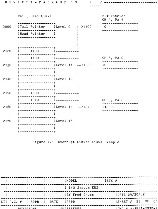
Interrupt requests are recorded in memory by placing the device's DRT entry on a linked list of devices requesting
interrupt service. There are sixteen such lists, one per
priority level, so the CPU can quickly locate an interrupting
device given its level. Figure 4.1 shows the list structure
in a situation where three device requests have been recorded.
The list links are stored in dedicated memory locations 2000-2171 (octal) as semaphores as well as absolute address
pointers. They are read using the read-and-set-to-minus-one
memory operation to insure that only one processor will have
access to a list at one time. The list head, if nonzero,
points to the first word of the DRT entry for the first device
in the list. The left half of this word is a link field
which, if nonzero, points to the first word of the DRT entry
of the next device in the list. The list continues until a
zero link field indicates the last entry. The list tail, if
nonzero, points to the first word of the DRT entry for the
last device in the list. Additional entries are made at the
end of the list.
The sequence of operations that the lOP performs to request
an interrupt of the CPU is given below. Calculation of the
device number, interrupt request message, and priority level have been described earlier.
1. Read and set to -1 the list tail for the level of the
interrupting device until the value read is not -1.
2. Send the interrupt message to the CPU.
IMODEL :STK #
:~~+--~~~~~-~+-~---~~+~--~-~~~-+~---~~~--~-~~~--~-+--~~-~-~~-~-~~--~-~~~--~~~-~
I I 1/0 System ERS
:BY Fred Gross IDATE 09/20/82
:--+~~~~-~~-~+~--~~--+~.-~~~--~+~-~~--~~~~---~~---~--~~+-~---~---~-~---~~-~~-:
:LT: P.C. # I APPR DATE ;APPD :SHEET # 21 OF 80
+~~~~-.~~-~~-~-~-~--~-.-~~-~~--~~-~-~~---~-~
/ /
lOERSI hp 1
HEW LET T - PAC K A R D C O. I 1
---+
3.
If the value is not zero, store the address of the firstword of the interrupting device's DRT entry in the device's DRT entry link field pointed by the list tail and, lastly, store the address in the list tail pointer.
4. If the value is zero, store in the list head and, lastly,
the list tail the address of the first word of the interrupting device's DRT entry.
This sequence completes the lOP processing of an interrupt
request. Operation of the lOP resumes as if the request had
not occurred, except that the interrupt mask on the lOP now disables the device that requested from requesting again. Note that the interrupt request bit is cleared by lOP during the processing of an interrupt request.
I
MODEL :STK #:~~+~-~-~-~~~+~-~~-~-+~~~~~.--~+---~--.-~~-~~---~~+-~~~~-~---~~~~~~-~-~-~---~~
I : 1/0 System ERS
i 18Y Fred Gross :DATE 09/20/82
:~~+~~~~~-~--+-.--~~~+~~~.~~--~+~~~~-.-.~-~---~---~~~~-+---~~~----~-~~~--~~~-~~
lLTI P.C. # : APPR DATE IAPPD :SHEET # 22 OF 80
+-~.-~~-~~--~~~-~~~-~~~~-.--~---~-~---~---~~
/
I IOERSI hp I
HEW LET T PAC K A R D C O. I I
2000
2120
2130
2140
2150
2160
2170
Tail, Head Links
ITail Pointer 1 Level 0 +-)1100
IHead Pointer
+---+
11001---+
+---+
1100o
o
o
o
1200
1240
o
1---....
--+ILevel 11 +-)1200
: Level 12
: .. __ ... _ ... _ .. +
: ... - - ... -+
I Level 14
I I
+-)1240
+---~----+
o
o
ILevel 15o
DRT CH
Entries
4, PA 4
+---+
10CH 5, PA 0
10
CH
5,
PA 211200
+---...
~---~~-+Figure 4.1 Interrupt Linked Lists Example
IMODEL ISTK II
:~~+~~~~~~-~~+~.~~~~-+-~~~~~~~~+--~-~~---~---~~+~~~-~~~~-~-~~~~~-~-~-
...
--~-:I I I I : 1/0 System ERS
.+~~~-~~---+--~~~~-+--~---~--+~--~~-~-.-~---~.---~~~~+~---~~~--~~-~~~~--~-~~~:
: I :BY Fred Gross IDATE 09/20/82
:~~+~-~-~~-~
...
+-~-.--~+~~-~~--~-+~~~~~-~~~~-~~----~~.~~~+~~-~--.---~~.--...
~--~~~-:ILTI P.C. # APPR DATE IAPPD ISHEET # 23 OF 80
:~~+--~-~.~-~+~~~~-~~+--~.---+~~---
...
~~---~----~~~-~~.+~~~-~--~~---~~~~~--~~: [image:23.612.22.559.50.763.2]+~~~~~~~~-~~~~~~~-~-~~~~~-~~~--~~-~~
..
~~-~-~/ /
lOERSI
hpI
HEW LET T - PAC K A R D C O. I I
---+
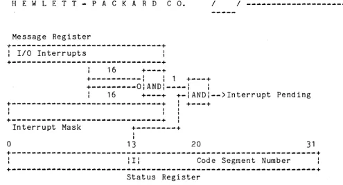
4.2 CPU OPERATIONS
4.2.1 Interrupt Masking
Although some very long machine instructions can be
interrupted, the CPU generally ignores liD interrupt requests
until the end of a machine instruction. At that time, if a
message bit corresponding to an liD interrupt has been set, if
the corresponding bit in the CPU Interrupt Mask is clear, if the interrupt enable bit (I) of the CPU Status register is set, and if no higher priority interrupt request or trap
exists, an
IIO
interrupt occurs. Figure 4.2 illustrates thismasking process except for the effect of higher priority interrupts and the lockout during machine instructions.
If an unmasked request at level n is the highest priority interrupt request, then an interrupt at level n is granted. The microcode interrupt handler will save the interrupt mask and then update the mask to disable interrupts from priority
levels n and lower. Levels higher than n which were
previously disabled will remain disabled. This mask will be
in place on entry to the service routine for the device at
level n. The old mask will be restored on exit from this
service routine.
~.2.2 Identifying the Interrupting Device
The sequence ~f operations that the CPU performs to obtain
the devic:e number of the device to be serviced is given below. The interrupt level to be serviced is that of the highest
priority message bit that was set and not masked, as described above.
1. Read and set to -1 the list tail for the level to be
serviced until the value read is not -1. Read the head
pointer. Since this is a pointer to a device's DRT entry, the
device number is found in bits 22-27.
:MODEL :STK #
:-~+~-~-~~--.+~~~-~~~+--~~~~~-~+~---~~~~--~~--~~~~+~~~-~~~-~--~-~-~--~--~~-~-~~:
I I I
I I : liD System ERS
I IBY Fred Gross IDATE 09/20/82
:~~+~~-.--~~~+-~-~~~~+~~~-~--~~+~-~~~~-~~--~~---~--~-~~+~~~~-_---.-M-~-~~~-~~_~
~LTI P.C. # I APPR DATE IAPPD ISHEET # 24 OF 80
...
+~~~~--~~~~~~-~~~~-
....
~----~--~.--~-~--~~~-~~-/ /
lOERSI hp I
HEW LET T - PAC K A R D C O. I I
---+
Message Register
: 1/0 Interrupts
o
Interrupt Mask
16
+---+
+---:
I 1+---+
+---OIANDI----1
:
: 16
+---+
+-IANDI-->Interrupt Pending+---+
I
I
13
I
I:
20
Code Segment Number
Status Register
Figure 4.2 CPU Interrupt Masking
31
2. Read the link field in the word pointed to by the list
head.
3.
Clear the message bit in the CPU message register for thelevel to be serviced if the link field was zero, indicating that no more requests are pending at that level.
4. If the link field was zero, store zero in the list tail.
If the link was not zero, store zero in the link field, store the link field in the list head, and, lastly, restore the tail pointer.
This process results in the removal of one device from the list of requesting devices and gives the CPU the device number required to access the DRT.
4.2.3 Reaching the Service Routine
The DRT entry contains pointers to the interrupt service
routine and variable area (See Figure 4.3). Using this
information, the microcode interrupt handler swaps out of the CPU the current program environment and sets up the
~-+-~--~~.--+~~~~~~-+~~---~~-~+---~----~~-~~~+~~~~-~~~~---~~~~~-~-~-~-~-~-:
: I : IMODEL :STK # :
:-~+~~~~~~~~~+-~~~~~~+~~-~-~~~-+~-~-~~--~~~-~~~~-
....
+~~---~~~~-~-~~--~~~~~---~~~~:: 1/0 System ERS
.+---~-.--~+~~~---~+-~-~--~-~+~~~--~~~-~~~--~--~--~--+~--~---~--~~~-~-~~-~:
: : :8Y Fred Gross IDATE 09/20/82
:--+~~-~-~---+-~~-~~~+-~-~
....
~--~+~~~~~~~~~~---~--~~~--~~+-~~-~--~-~-~-~~~~~~~~~~:\LT\ P.C. # : APPR DATE ;APPD ;SHEET # 25 OF 80 ;
;-~+~-~--~---+---~-.~+~~--~-~-~+~~~---~~--~--~--~--~---+~.--~~--~~----~~-.~~-~-:
+~~~~~~~-~~~-~-~--~.-~~~~~.~~-.~~-.-~.---~~~
/ /
lOERSt
I hp I
HEW LET T • PAC K A R D C O. I I
---+
environment of the service routine. Refer to the machine
instruction set ERS for the details of these CPU operations.
The interrupt service routine is entered with interrupts
disabled. The CPU interrupt mask has already been updated to
mask interrupt requests of equal or lower priority.
Main Memory
+---+
OOOH I System In fo. : 0000
+_ ... - ... ---_ ....
_+
080HlChannel 1 :0200
IDRT Entries
+---+
100HlChanne12 :0400
IDRT Entries
+ ... _ ... _ ... _+
180HlChannel 3 10600
IDRT Entries
+---+
200HlChanne14 11000
IDRT Entries
+---+
280HIChannel5 \1200
lDRT Entries
+ ... _ ... _ ... +
300HlChannel 6 11400
lDRT Entries
+ ... +
380HlChannel1 \1600
lDRT Entries
+---_ ... +
400HlHead
&
Tail 12000IPtrs(16 Lvls)1
+---+2200
+---+
Device 0\Device 1: Device 2\ Device 3\ Device 41
Device 51
IDevice 6\
IDevice 1:
+---+
ILink O. S. In fo • I
lData Segment IPointer
IInterrupt Service IRoutine Pointer
+ ...
_---+
IMPB Command List ptrl
Figure 4.3 DRT Entries
4.2.4 Interrupt Routine Exit
At the completion of the service routine, the CPU microcode for the interrupt exit instruction restores the environment of
IMODEL ISTK II
: 1/0 System ERS
.+~----~~~-+-~~-~
...
~+-~-... ---+-..
~~~~-~-~~-.~--~-~~---+~-~-~~~.--...
~..
~...
-~~~~~-~:I 18Y Fred Gross IDATE 09/20/82
:~-+~-~~~~~~-+---~--~+~~~~~~.~~+~-~-~-~-~-~~~-~-~~~~~~~+~.--~.~---~.~-~~---~~-~:
ILTI P.C. # I APPR DATE IAPPD ISHEET # 26 OF 80
[image:26.613.32.574.156.783.2]+~---.~~~~-~~~~----~~-~~-~--.~~~~~-~.--~-~--
/ /
IOERSI hp I
HEW LET T - PAC K A R D C O. 1 I
---+
the interrupted program or the environment of the dispatcher. Refer to the Machine Instruction Set ERS for the details of
I these CPU operations.
Interrupt service routine exit has no effect on the 1/0
channels or the interrupt request structure except that the CPU interrupt mask corresponding to the interrupted progm (or dispatcher) is restored.
4.3 MPS COMMAND EXECUTION BY lOP
MPS commands can be executed by the lOP independent of the
CPU. A bit in each status register for each PA specifies
whether an interrupt will be sent to the CPU or whether the lOP will execute an MPS command from a list in memory.
The command list location is stored as the fourth word of
the DRT. It is updated as the commands are executed. The
command lists consist of pairs of command followed by one or
two data words. One Write or Control command is executed each
poll cycle where no higher PA is requesting service. Read
commands are not allowed in the command list, since using them
will cause unexpected channel communication. For the Write
Interface and Read Interface & Record commands, the PA field
is taken from the command word when executing the command. All other commands use the PA from the channel executing the command.
If a skip command is executed, that PA will be disabled from executing commands (or posting interrupts) until a poll cycle of no activity (i.e. no DMA's, no interrupts, no other PA
command execution, no RAMD request). The Skip Mask is located
in the lower eight bits of the Interrupt Message register.
The interrupt request bit must be set or the interface must
respond to a poll to activate Command Execution. A Status
false during DMA will cause the Command Execution bit in the
status register to be cleared. Commands in a list must have
the correct PA in the appropriate field.
The execution times for commands executed by
rop
areapproximately from one every
76
states to one every104
statesfor most instructions.
4.4 ATTENTION REQUESTS
I
I
:-~+--~~~-.~~+~-~~-~~+-~--~~~~-+~----~~--~~~~~~~~-+~~~~~--.----~~~-~~~~~~-~~~~-:
: : : : :MODEL lSTK #
:~~+~~-~~-~~~+~~---~~+~~~~~~~~~+~~-~~~~~~~~~~~----+--~~~~~--~~-~~-~~---~-~--~~~:
I : : : 1/0 System ERS
.+--~~----~+~.--~.~+~.~-~~~--+~---~---~--~~---~--~~+---~~~~~-~-~~~~~~~-~~~~:
:
:SY
Fred Gross lDATE 09/20/82:--+~~---~~-~+~~~-~~-+~-~~-~~--+~~~~--~~~~-~-~--~~-~~~~+--.~--~~~~~~-~~~~~-~~~~:
ILTI P.C. # ~ APPR : DATE \APPD :SHEET # 27 OF 80
+~~~-~~----~~-~----~~-~~--~~~~~--~-~~-~-~-~~
/ /
lOERSI hp I
HEW LET T - PAC K A R D C O. I I
---+
During a Service Request Poll cycle (INT true) assertion of
ASYNC will be treated as a request for an Attention Poll. If
there is no response to the Service Request Poll and if RAMD is not asserted, then ASYNC will be tested for an Attention
Poll Request. If true, IC4 (BP[1]) will be set true with INT
true for an Attention Poll.
A poll response will be latched and priority encoded
according to PA. The winning response (if any) will then
receive a write of 1 to FR1 (IC=0001). This corresponds to an
Attention Request Disable. If no device responds to the Poll,
lOP will just continue with Service Request Polls.
The PA receIvIng an ARD will be logged in TFO(16:8)
according to PA. A mask (in TFO(0:8» is used during the
Attention Poll to exclude any unwanted PA's. See CSG 1/0
Standards for further details.
lMODEL lSTK #
: 1/0 System ERS
.+~~~-~~~~-+-~~~-~~+~~~~~~~--+~--~~~-~~~~~-~-~~~~~~~-+~~---~~-~~~~~~~~~~~~-~~:
:BY Fred Gross IDATE 09/20/82
I
:-~+~~~~~~-~~+~~--~~-+~----~~~-+--~-~---~~-~-~~--~-~-~-+-~~----~~-~--~~~-~~~~~-:
ILTI P.C. # I APPR DATE IAPPD ISHEET # 28 OF 80
:~~+._~~~~._~+-~.-~-~+---~~~~~~+---~~M-~~~-~----~-~~-~~+~~~.~~---~---~~~-~~-~~-:
+~~~--~-~~~-~--~-~~~-~~-~-~-~.~-.---~~~-~~-~
/ /
IOERS,.
I hp I
HEW LET T - PAC K A R D C O. I I
---+
5. MPB 1/0 COMMANDS
Transfer of commands and data between the CPU and lOP is done
with MPB channel-to-channel operations. These transactions
consist of sending a channel address and a single data word in
primary mode over the MPB for a WRITE operation. The return
address for the requested data word is contained in the channel
address for READ instructions. The write of data back to the CPU
is done in secondary address mode. A third type of 1/0 command
does not require a data word at all. These CONTROL operations are
like WRITE's except a zero data word is sent and ignored by the lOP.
The lOP interprets the channel address as an 1/0 command and
uses or returns a data word based on that command. The format of
the channel address for an 1/0 command is given in Figure 5.1.
Not all of the fields are used by the lOP for every operation but
they exist for uniformity. Only the lOP whose channel number
appears in the channel number field receives and executes the command.
NOTE: The bit positions in the commands refer to the MPB channel
address and data words. The CPU shifts the lOP command bit fields
and forms the MPB 1/0 Commands in microcode.
Figure 2.1 showed that the MPB commands are executed
)eriodically by the lOP. Until execution of a command is begun,
, the lOP will not accept another command.
The MPB commands are listed below with their operation codes in
octal. In all cases the format of Figure 5.1 is used. After the
name of each command is a R, W, or C to indicate whether the
operation is a READ, WRITE, or CONTROL. Additional commands for
lOP command execution are unlabeled. Figure 5.2 contains a
summary of the commands. Undefined op codes will cause a message
to be sent (bit 7) to the CPU and otherwise be ignored.
The MPB commands are addresses each pointing to 1 of 128 words
of control store on lOP. The first 128 words form a jump table to
the actual command routine to allow adjustments in lOP microcode without affecting MPB command code assignments.
5.1 DMA COMMANDS
5. Write DMA Start Address (W) WDA
IMODEL :STK #
:-~+-~~~~~~~~+~~~~~~~+~~-~~-~-~+~~~~~~~--~--~~~~~~+~-~--~~~---~~~-~~~-~~~~~~~~~I
I 1/0 System ERS
:BY Fred Gross IDATE 09/20/82
:~~+~-~~-~~~-+-~~-~~-+-~~~---~-+~-~~-~-~~-~~~~-~-~~-~~~+~-~---~~-~~-~~~~~~~~
ILT: P.C. II : APPR DATE \APPD ISHEET # 29 OF 80
+~~~~~---~~~.~-~-~~~-~~~----~-.~.-~-~~~-~~-~
/ /
lOERSI hp I
HEW LET T - PAC K A R D C O. I I
---.---+
The data word is loaded into the Address register
corresponding to the PA in the channel address. It is
interpreted as an absolute byte address and for halfword DMA must lie on a halfword boundary.
6. Write DMA Termination Field (W) WDTF
The data word is loaded into the TF register corresponding to
the PA in the channel address. For byte input bits 24-31
specify the termination byte. Any bits in the data word 0-23
will disturb the adjacent termination field or other data in the TF register.
3. Write DMA Status (W) WDS
The data word is loaded into the CCST register bits 16-20,
25-31 corresponding to the PA in the channel address. The
interrupt field is assumed zero and the old level is
unchanged. Since the DMA status bits control DMA operation,
this command should only be used when DMA is disabled. Table
5.1 lists the status bits and their meanings.
4. Write DMA Count (W) WDC
The data word is loaded into the Count register corresponding
to the PA in the channel address. Bits 16-31 are interpreted
as the 16 bit integer length of the DMA block transfer in
transfers.
23. Start DMA (C) SD
A bit in the DMA Mask register corresponding to the PA in the
channel address is set to a one. If the DMA is an input, the
First Input Pending bit is set. If the DMA is an output or a
verify, a data word or byte prefetch is done.
17. Start DMA, Enable Interrupt, Clear IRQ (C) SDEC
Identical to Start DMA except a bit in the Interrupt Mask
register corresponding to the PA in the channel address is set to a one and the corresponding Interrupt Request bit is
IMODEL :STK #
:~~+~-~--~--~+~~~~~--+~--~~~~--+~---~~~.-~~--~~~~~+--~-~-~~-.~-~~~~~~~~~~~~-~~~;
I
: 1/0 System ERS
.+--~-~--~-+-~~.--~+~-~-~~~~~+~-~~~--~~-~-~---~-~~~~~+~~~~-~---~~~--~~~~~-~~-:
I : 18Y Fred Gross IDATE 09/20/82
,
:~-+-~-~-~--~+-~~-~~~+~-.~~-~~~+~---~-~-~~.-~~~-~~~~~~~+~~~~~----~-~~~--~-~-~~-:
ILTl P.C. # : APPR : DATE lAPPD :SHEET # 30 OF 80
:-~+-~-~~~--~+~-~~.~-+--~--~~--+~~---~-~-~-~~--~~~~--+~~~-.-~~.-~~~~-~~~~~--~:
I
+-~~~-~----~~~~~~~~~.~-~----~~~--~~--~-.~~--
/ /
IOERS/ hp /
HEW LET T - PAC K A R D C O. / /
---+
o
cleared.
Bit
16 17
18
19 20 21-24 25 26
27
28 29 30 31
Meaning
DMA Terminated on STS False
DMA Terminated on Match or Verify Error DMA Terminated on Count Zero
Suppress Channel End on Burst DMA MPB Command Execution by lOP
Interrupt Level for Device First Input Transfer Pending
Assert Channel End on Multiplex DMA
F1 F1=0 F2=0 Input F1=0 F2=1 Input, Term.
on Match
F2 F1=1 F2=O Output F1=1 F2=1 Input, Verify
Byte (=1)1 Halfword Transfers
Not used
DMA Terminated on Device End
Table 5.1 DMA Status Bits
3 6 9 13 19 22 25 31
: 1 0 1 I Ch • No: PA IC :X X X X X X:CPUcnIX X XI lOOp Code Figure 5.1 MPB Command Format
20. Start DMA, Clear IRQ (C) SDC
Identical to Start DMA except a bit in the Interrupt Request register corresponding to the PA in the channel address is cleared.
15. Enable DMA (C) EDMA
The bit in the DMA mask corresponding to the PA in the channel address is set to enable DMA for the PA.
16. Disable DMA (C) DDMA
The operations are the same as for ENABLE DMA except the bit
is cleared to disable DMA for the PA. This termination of DMA
does not cause an interrupt request bit to be set.
:~~+~~~-~~~~~+~--~~-~+~-~~-~~-~+-~---~~~~~~~~-~.~-+-~~--~~~~~~-~~~~-~~--~~~~-~~
: IMODEL :STK #
:--+~~~~-~~~~+~~~~~-~+--~-.----+~~~~--~~-~~-~~~-~-+~~~--~-.~--.~~~~~~~~~-~-~~~~
I : 1/0 System ERS
IBY Fred Gross :DATE 09/20/82
:--+~~--~~~~~+~~-~-~-+~~~~--~~~+.----~--~~~-~----~--.--+---~----~~~--~~-~~~~~.~
ILT: P.C. # ~ APPR DATE IAPPD ISHEET # 31 OF 80
:-~+~~-~-~~--+--~-~--+~-~---~~~+~-~~.---~~--~~.---~~~~~+~~~~--·--~~~~~~~·~~~~~~t
[image:31.615.25.531.43.759.2]+~~~~~-~-~---~~~~~~~~~-~-~~---~~~--~~~~~~~
/ /
IOERS/ hp /
HEW LET T - PAC K A R D C O. / / ______________________ A _ _ _ _ _ _ +
Read OMA Current Address (R) ROA
The contents of the Current Address register corresponding to
the PA in the channel address are returned to the CPU. It
should be interpreted as the byte address of the datum
following the datum to be output next for output and as the byte address of the datum last input (or the starting address if no inputs have occurred) for input.
10. Read OMA Current Count/Status (R) ROCS
The contents of the CCST register