A Novel Design of Half and Full Adder using Basic QCA
Gates
Subhashee Basu
St Thomas College of Engineering and Technology 4 Diamond Harbour Road
Kolkata 700023,India
Aditi Bal
St Thomas College of Engineering and Technology 4 Diamond Harbour Road
Kolkata 700023,India
Supriyo Sengupta
St Thomas College of Engineering and Technology 4 Diamond Harbour Road
Kolkata 700023,India
ABSTRACT
This paper presents the novel design of half adder and full adder us-ing reduced number of QCA gates.This design utilizes the unique characteristics of QCA to design a half and a full adder.The basic component of QCA is a cell consisting of two electrons and four logically interacting quantum dots.Simulation indicates a fast,efficient and very attractive performance(i.e.complexity,area and delay)
Keywords:
QCA, half adder,full adder
1. INTRODUCTION
VLSI technology,although has made remarkable progress in the past,this progress may be slowed down in future.Among the chief technological limitations for this slowdown are the interconnect problem and power dissipation. As more and more devices are packed into the same area, the heat generated can no longer dis-sipate and may result in damage to the chip. QCA[2, 3, 6, 10, 17] provides a good alternative to the silicon technology.QCA based circuits have the advantage of high speed, high integrity and low power consumption. Also Q QCA circuits have the advantage of high parallel processing.
Adders are basic circuits in digital logic.Conventional transistor based adder circuit requires many wires.Due to the delay caused by these wires,most of the previous adder circuits are limited in speed.Moreover,such complex circuits are difficult to implement in QCA [1, 4, 5, 7, 8, 9, 10, 11, 12, 16, 17, 18, 19, 20].Adder performance can be enhanced by minimizing the carry propaga-tion delay.Many designs of adder using QCA have already been proposed[13, 14, 15]. This paper presents a design of adders that is optimized for implementation in QCA.
2. QCA DESIGN SCHEME
The quantum dot cellular automata use a binary representation of information, by replacing the current switch with a cell having a
bistable charge configuration. One configuration of charge repre-sents a binary ”1”, the other a ”0”. The field from the charge con-figuration of one cell alters the charge concon-figuration of the next cell. Remarkably, this basic device-device interaction is sufficient to support general purpose computing with very low power dissi-pation.
2.1 QCA Cells
[image:1.595.411.460.525.567.2]A QCA cell[3] possesses an electric quadrupole which has two sta-ble orientations as shown in Fig.1 . These two orientations are used to represent the two binary digits, ”1” and ”0”.A QCA cell com-prise of four quantum-dots arranged in a square pattern. The cells contain two mobile electrons(or holes) which repel each other as a result of their mutual Coulombic interaction and in the ground state tend to occupy the diagonal sites of the cell. These lead to two po-larizations of a QCA cell, denoted as P=+1 and P=-1 respectively. Thus logic 0 and logic 1 are encoded in polarization P=+1 and P=-1 respectively. When a second cell is placed near the first cell, the coulomb interaction between the cells removes the degeneracy and determines the ground state of the first cell.
Fig. 1. Basic QCA cell and Two Possible Polarizations
2.2 QCA Wires
activated cells to be polarized. Thus, signals propagate from one clock zone to the next.
Fig. 2. QCA wire
2.3 QCA Gates
Majority voter gate and inverter acts as the basic gates in QCA. The governing equation of majority voter gate is
M(A, B, C) =AB+BC+AC (1)
Two input AND and OR gate can be implemented from three input majority voter gate by making one input constant.
M(A, B,1) = A+B
[image:2.595.82.545.92.770.2]M(A, B,0) = AB (2)
Fig 3 and Fig 4 shows the gate symbols and their layout.
Fig. 3. QCA Majority Voter Gate
Fig. 4. QCA Inverter Gate
3. ADDER CIRCUITS
A half adder performs the addition of two boolean variables and gives two output,one is the sum and the other is the carry.Let A ad B be two input variables.Then the sum and carry is respectively given by
S = A⊕B
C = AB (3)
The truth table of half adder is given in table1.
Table 1. Truth table of Half Adder
A B S C 0 0 0 0 0 1 1 0 1 0 1 0 1 1 0 1
The circuit diagram of half adder is given below.
Fig. 5. Circuit Diagram of Half adder
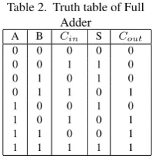
The full adder performs the addition of three boolean variables and produces two outputs,a sum and a carry.Let A,B and C are three variables.Then the sum and carry is respectively given by
S = A⊕B⊕C
C = AB+BC+CA (4)
[image:2.595.382.491.580.693.2]The truth table of full adder is given in table2.
Table 2. Truth table of Full Adder
A B Cin S Cout
0 0 0 0 0
0 0 1 1 0
0 1 0 1 0
0 1 1 0 1
1 0 0 1 0
1 0 1 0 1
1 1 0 0 1
The circuit diagram of full-adder is given below.
Fig. 6. Circuit Diagram of full adder
3.1 Proposed method
[image:3.595.351.579.264.382.2]In order to realize half adder using QCA,we need three majority gate and an inverter.The two input A and B are fed simultaneously into two majority gates 1 and 2 ,one of which acts as an AND gate and another acts as an OR gate.The output of the AND gate is fed into an inverter and finally,the outputs of majority gate 1 and that of the inverter are fed into another majority gate 3.The output of ma-jority gate 3 is the sum and that of mama-jority gate 2 is the carry.The circuit diagram and the layout is given in figure 7 and 8.
Fig. 7. Circuit Diagram Half adder using QCA gates
Fig. 8. Layout of Half adder using QCA gates
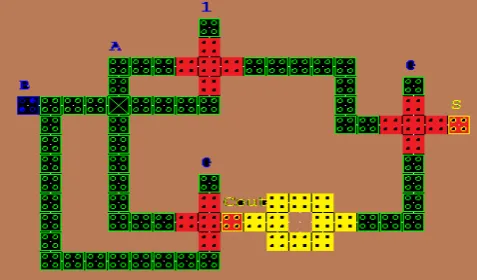
If one observe carefully,one will see that the half adder circuit is nothing but a XOR gate which is realized using QCA basic gates. Full adder can be implemented using only two majority gate and an inverter.Majority gate 1 is a five input majority gate,whose three inputs are A,B,C and the other two inputs are shorted to the output of the inverter.The output of majority gate 1 is the sum.Majority gate 2 is a three input majority gate.A,B,C acts as the inputs to majority gate 2 and the output is the carry.The output of majority gate 2 is also fed into an inverter whose output goes into majority gate 1 as mentioned above.The circuit diagram and layout is shown in figure 9 and 10.
[image:3.595.70.305.393.481.2]It is to be noted that in figure 8 and 10,the red portion indicates the QCA majority gates,the yellow portion indicates the inverters and the rest are the QCA wires.The cross symbol indicates the crossover of two wires.
Fig. 9. Circuit Diagram of full adder using QCA gates
[image:3.595.318.558.459.641.2] [image:3.595.54.293.532.672.2]4. RESULT ANALYSIS
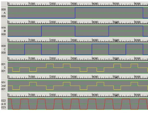
[image:4.595.53.296.175.320.2]The number of gates required to realize half and full adder is min-imal.If we compare our results with [1],it will be seen that our proposed method reduces the number of gates required compared to [1].Consequently,the area,complexity and delay of the circuits will also reduce and hence,the performance of the circuit will in-crease.The simulation result of half adder and full adder obtained by simulation the layouts in QCADesigner is given in figure 11 and 12.
Fig. 11. Simulation result of Half Adder
Fig. 12. Simulation result of Full Adder
5. CONCLUSION
Although this method is assumed to be implemented in metal-based QCA implementation,the underlying principles also apply to molecular QCA. There are different clocking schemes such as wave clocking which may be more suitable for molecular QCA. If the manufacturing issues of molecular QCA can be solved, it may be an attractive implementation alternative that mitigates the cryogenic working temperature constraints of metal based QCA. Molecular QCA is considered to be the only feasible implementa-tion method for mass producimplementa-tion of QCA devices.
6. REFERENCES
[1] Ja’Ja’, S.M.Wu.,” A new approach to realize partially symmet-ric functions”.Tech.Rep.SRCTR86-54, Dept.EE, University of Maryland, 1986.
[2] C. S. Lent, P. D. Taugaw, W. Porod , G. H. Berstein.,” Quantum Cellular Automata.Nanotechnology”, vol. 4, no. 1, pp49-57,January 1993.
[3] A. O. Orlov, I. Amlani, G. H. Bernstein, C. S. Lent, G. L.Sinder.,” Realization of a Functional Cell for Quantum Dot Cellular Automata”, Science, vol. 277, no. 5328, pp 928-930,August 1997.
[4] C. S. Lent, P. D. Taugaw.” A Device Architecture for Comput-ing with Quantum Dots”, ProceedComput-ings IEEE, vol. 85, no. 4, pp.541-557,April 1997
[5] I. Amlani, A. O. Orlov, G. Toth, C. S. Lent, G. H. Bernstein, G. L.Sinder.,” Digital Logic Gate using Quantum Dot Cellular Automata”, Science, vol. 284, no. 5412, pp. 289-291,April 1999.
[6] M. Lieberman, S. Chellamma, B. Varughese, Y. Wang, C. S. Lent, G.H. Bernstein, G.L.Snider, F. Peiris.,” Quantum Dot Cellular Automata at a Molecular Scale”, Annals of the New York Academy of Sciences, vol. 960, pp. 225-239,2002.
[7] Whitney J. Townsend, Jacob A. Abraham.” Complex Gate Implementations for Quantum Dot Cellular Automata”, 4th IEEE Conference on Nanotechnology , pp. 625-627,August 2004.
[8] R. Zhang, K.Walus, W.Wang, G.A.Jullien.,” A Method of Majority Logic Reduction for Quantum Cellular Automata”, IEEE Trans on Nanotechnology, vol. 3, no. 4, pp. 443- 450, Dec 2004.
[9] K. Walus, G. Schulhof, G. A. Jullien, R. Zhang, W. Wang.,” Circuit Design Based on Majority Gates for Application with Quantum Dot Cellular Automata”, IEEE Trans Signals, Systems and Computers, vol. 2, pp. 1354-1357,Nov 2004.
[10] M. Momenzadeh, M. B. Tahoori, J. Huang, F. Lom-bardi.,” Characterization, Test and Logic Synthesis of AND-RINVERTER (AOI) Gate Design for QCA Implemen-tation”,IEEE Trans on Computer Aided Design of Integrated Circuits and Systems, vol. 24, no.,pp. 1881-1893, December 2005.
[11] H. Rahaman, B. K. Sikdar, D.K. Das.” Synthesis of Symmet-ric Boolean Functions Using Quantum Cellular Automata”, International Conference on Design and Test of Integrated Systems in Nanoscale Technology (DTIS 06), pp.119-124, Tunis, Tunisia.
[image:4.595.52.294.361.547.2]Computation, Vol. 0,No. 0000-000c Rinton Press,2008.
[13] Mostafa Rahimi Azghadi*, O. Kavehei, K. Navi.”A Novel Design for Quantum-dot Cellular Automata Cells and Full Adders”
[14] Heumpil Cho.” Adder Designs and Analyses for Quantum-Dot Cellular Automata”, IEEE Transactions on Nanotechnol-ogy, Vol. 6, No. 3, May 2007
[15] Heumpil Cho, Earl E. Swartzlander.” Adder and multiplier Design in Quantum-Dot Cellular Automata”, IEEE Transac-tions on Computers, Vol. 58, No. 6, Jun 2009
[16] Geza Toth* , Craig S. Lent.” Quantum computing with quantum-dot cellular automata”, Physical Review A, Volume 63, 052315
[17] Pijush Kanti Bhattacharjee.” Use of Symmetric Functions Designed by QCA Gates for Next Generation IC”, Interna-tional Journal of Computer Theory and Engineering, Vol. 2, No. ,April 2010 1793-8201
[18] Hema Sandhya Jagarlamudi, Mousumi Saha, Pavan Ku-mar Jagarlamudi.” Quantum Dot Cellular Automata Based Effective Design of Combinational and Sequential Logical Structures”, World Academy of Science, Engineering and Technology 60, 2011.
[19] C.Rovetta , M.Mouffron.” De Bruijan sequences and com-plexity of symmetric functions”, Cryptography and Communi-cations journal, vol.3, no. 4, pp.207-225,(December,2011).