Area and Performance Evaluation of Central DMA
Controller in Xilinx Embedded FPGA Design
Amruta Shete1, Kajal Kumbhar2, Shubhangi Mane3, Rupali Rakibe 4 1, 2, 3, 4
Department of Electronics & Telecommunication, Engineering, Bhivarabai Sawant Institute of Technology and Research, Wagholi, Pune.
Abstract: Steady treatment of a great deal of data is required in each electronic banner dealing with errand performed on FPGAs. Powerful, high throughput and low overhead trade of data between sub-modules in a FPGA based embedded system can be a trying issue. Availability of sensitive and hard CPU focuses, their related system and change gadgets for FPGAs, give us the probability of making an aggregate system on a single FPGA. Different DMA transfer techniques provide sub-modules with the possibility of high performance data transfer without CPU intervention. Focusing on Xilinx FPGA devices which contain PowerPC hard CPU core, we have performed a detailed study of a DMA transfer technique based on central management of data movements. Data transfer performance of the system is evaluated carefully in different scenarios, thus proving the effectiveness of exploiting central DMA controller in practical applications. Linux is the dominant OS in most of FPGA based embedded systems. Simplified management and utilization of central DMA transfers can become feasible by the means of suitable kernel mode drivers.
Keywords: Embedded Systems, PowerPC hard core, DMA transfer, Real-time data processing, Linux drivers.
I. INTRODUCTION
FPGA based Embedded Systems usually contain one or multiple CPU cores, memory controllers, interrupt handlers and different sets of peripherals. The ensemble of CPU, peripherals and buses, that connect system parts together, is called a base system. Several hard and soft CPU cores are introduced by famous FPGA manufacturer companies during recent years. Most notable ones are Alter a NIOS, Xilinx Micro Blaze which are soft core CPUs and PowerPC, hard core CPU available in Xilinx high-end FPGAs. In a FPGA based embedded system, however, there are limited number of buses with pre-defined protocols and all of the peripherals, memory controllers and CPUs reside on these busses.
There exists a specialized FPGA design tool, which allows users to create a fully functional system with all of the required interfaces and debugging facilities easily. Each of the peripherals requires an initialization procedure, which should be done by the CPU. They also need to be commanded and controlled to perform necessary transactions when required. This is mostly done under the supervision of the CPU. In the simplest case, the system operates in standalone mode. In this case peripheral drivers are just simple library routines, included in the main application.
There is no multitasking or intelligent memory management in standalone mode. In the second case CPU can execute an operating system (OS).The OS provides complete functionality such as scheduling and memory management. It also provides complete APT libraries for handling network, file-systems, various block and character devices, user interfaces and so on. Write operation to the file transfers data to peripheral and read operation receives data from it.
Peripheral control operations get extremely simple using the driver. An operating system is a vital part of every complicated embedded design, because it provides various protocol stacks, ready to use drivers and APT’s. User is no more required to be worry about handling network, different file-systems, talking to USB devices and managing user interfaces. The custom module is required to talk to the rest of the system using shared busses. While naturally every data transmission is handled by CPU, in many cases we prefer to transfer data between two nodes without CPU intervention.
A. Need of project
B. Objective of the Project
1) Area and Performance Evaluation of Central DMA Controller in Xilinx Embedded FPGA Designs.
2) Area Consumption of DMA should be as low as possible.
3) Combinational Path should be very low.
4) High Throughput.
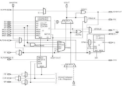
[image:3.612.115.498.164.318.2]II. BLOCKDIAGRAMOFPROPOSEDSYSTEM
Fig 3.1 Block diagram of Proposed System
C. Block Diagram Explanation
1) DMA Controller: Direct Memory Access (DMA) is one of several methods for coordinating the timing of Data transfers between an input/output (I/O) device and the core processing unit or memory in a computer. DMA is one of the faster types of synchronization mechanisms, generally providing significant improvement over interrupts, in terms of both latency and throughput. An I/O device often operates at a much slower speed than the core.1 DMA allows the I/O device to access the memory directly, without using the core. DMA can lead to a significant improvement in performance because data movement is one of the most common operations performed in processing applications. Traditionally DMA uses the same internal address data buses at the core. The DMA unit contains the necessary counters, offset registers, and pointers to transparently handle one, two, three dimensional data matrix transfers. Direct memory access (DMA) is a method that allows an input/output (I/O) device to send or receive data directly to or from the main memory, bypassing the CPU to speed up memory operations. The process is managed by a chip known as a DMA controller (DMAC).
2) ADC: There are many methods to convert analog signals to digital signals. These converters find more applications as an intermediate device to convert the signals from analog to digital form, displays output on LCD through a microcontroller. The objective of an A/D converter is to determine the output signal word corresponding to an analog signal. Now we are going to see an ADC of 0808. It is an 8-bit converter with 5V of power supply. It can take only one analog signal as input. The digital output varies from 0-255. ADC needs a clock to operate. The time taken to convert the analog to digital value depends on the clock source. An external clock can be given to CLK IN pin no.4. A suitable RC circuit is connected between the clock IN and clock R pins to use the internal clock. Pin2 is the input pin – High to low pulse brings the data from internal register to the output pins after conversion. Pin3 is a Write – Low to high pulse is given to external clock. Pin11 to 18 are data pins from MSB to LSB.
3) UART (RS232: A universal asynchronous receiver-transmitter (UART) is a computer hardware device for asynchronous serial communication in which the data format and transmission speeds are configurable. The electric signaling levels and methods are handled by a driver circuit external to the UART. A UART is usually an individual (or part of an) integrated circuit (IC) used for serial communications over a computer or peripheral device serial port. UARTs are now commonly included in microcontrollers. A related device, the universal synchronous and asynchronous receiver-transmitter (USART) also supports synchronous operation.
4) PC: We are using MATLAB software on PC. Role of MATLAB is just to send and receive data from FPGA. We will create one user friendly GUI for loading and writing data from and to FPGA.
PC
5) FPGA: FPGA stands for field programmable gate arrays that can be configured by the customer or designer after manufacturing. Field programmable gate arrays are called this because rather than having a structure similar to a PAL or other programmable device, they are structured very much like a gate array ASIC. This makes FPGAs very nice for use in prototyping ASICs, or in places where an ASIC will eventually be used .For example, an FPGA may be used in a design that needs to get market quickly regardless of cost. Later an ASIC can be used in place of the FPGA when the production volume increases, in order to reduce cost. FPGAs are programmed using a logic circuit diagram or a source code in a hardware description language (HDL) to specify how the chip will work. FPGAs contain programmable logic components called "logic blocks", and a hierarchy configurable interconnects are called switch boxes. Logic blocks can be configured to perform complex combinational functions, or merely simple logic gates like AND and XOR. In most FPGAs, the logic blocks also include memory elements, which may be simple flip-flops or more complete blocks of memory. FPGA provides the next generation in the programmable logic devices. As compared to standard gate arrays field programming gate arrays are larger devices. A FPGA is a device that contains the metrics of reconfigurable gate array logic circuitry. When FPGA is configured the internal circuitry is connected in way that creates hardware implementation of software application. Unlike processors, FPGA use dedicated hardware for processing logic and do not have an operating system. FPGA’s are truly parallel in nature so different processing operation do not have to complete or the same resources. As a result, performance of one part of application is not affected when additional processing is added. Also multiple control loops can run on single FPGA device at different rates. A single FPGA can replace thousands of discrete components by incorporating millions of logic gates in single integrated circuit chip.
III. CONFIGURABLELOGICBLOCKS
[image:4.612.104.494.432.707.2]Configurable Logic Blocks contain the logic for the FPGA. In large grain architecture, these CLBs will contain enough logic to create a small state machine. In fine grain architecture, more like a true gate array ASIC, the CLB will contain functions. It also contains flip-flops for clocked storage elements, and multiplexers in order to route the logic within the block, to and from external resources. The multiplexers also allow polarity selection and reset and clear input selection.
A. Hardware Description 1) Spartan 6 FPGA
Fig 2. Spartan 6 FPGA
B. Features
1) FPGA: Spartan XC6SLX9 in CSG324 package
2) DDR: 166MHz 512Mb LPDDR (MT46H32M16LF/W949D6CBHX6E)
3) Flash memory: 16 Mb SPI flash memory (M25P16)
4) USB 2.0 interface for On-board flash programming
5) FPGA configuration via JTAG and USB
6) 8 LEDs Six Push Buttons and 8 way DIP switch for user defined purposes
7) VGA Connector
8) Stereo Jack
9) Micro SD Card Adapter
10) Three Digit Seven Segment Display.
11) 32 IOs for user defined purposes
12) Four 6×2 Expansion Connectors
13) On-board voltage regulators for single power rail operation
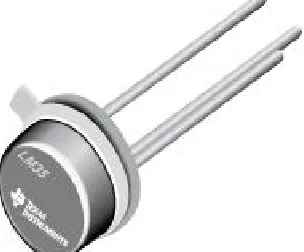
C. Analog sensor for ADC 1) LM 35 Temperature Sensors
Fig 3. LM 35 Temperature Sensors
D. Features
1) Calibrated Directly in Celsius (Centigrade)
2) Linear + 10-mV/°C Scale Factor.
[image:5.612.247.399.519.645.2]4) Rated for Full −55°C to 150°C Range.
5) Suitable for Remote Applications.
6) Low-Cost Due to Wafer-Level Trimming.
7) Operates from 4 V to 30 V.
8) Less than 60-µA Current Drain
Fig 4. 16*2 LCD Display
LCD is an electronic Show LCD is an electronic showcase module and fined an extensive variety of uses. A 16x2 LCD presentation is extremely fundamental module and is generally utilized as a part of different gadgets and circuits.
E. Features
1) Display Format: 16 Character x 2 Line
2) Viewing Direction: 6 O’clock
3) Input Data: 4-Bits or 8-Bits interface accessible Display Font
4) Display Font : 5 x 8 Dots
5) Power Supply : Single Power Supply
6) Backlight LED
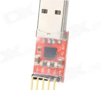
[image:6.612.201.444.153.327.2]7) USB to Serial converter
Fig 5. USB to Serial Converter
[image:6.612.238.415.513.668.2]F. Features
1) Single-Chip USB to UART Data Transfer
2) Integrated USB transceiver; no external resistors required
3) Integrated clock; no external crystal required
4) USB Function Controller
5) USB Specification 2.0 compliant; full-speed (12 Mbps)
IV. SOFTWAREDESCRIPTION
A. Xilinx ISE 13.1
Xilinx ISE (Integrated Synthesis Environment) is a software tool produced by Xilinx for synthesis and analysis of HDL designs, enabling the developer to synthesize("compile") their designs, perform timing analysis examine RTL diagrams, simulate a design's reaction to different stimuli, and configure the target device with the programmer. Xilinx ISE is a design environment for FPGA products from Xilinx, and is tightly-coupled to the architecture of such chips, and cannot be used with FPGA products from other
vendors. Step by Step procedure to run a program on FPGA board:
B. MATLAB
MATLAB R2013.a version and image processing toolbox is used. MATLAB is a high-level state specialized registering language and intelligent environment for calculation advancement, information representation, information examination and numeric calculation. Utilizing the MATLAB item, we can tackle specialized registering issues quicker than with customary programming dialects, for example, C, C++ and FORTRAN. MATLAB is an incorporated specialized registering environment that consolidates numeric calculation, propelled design and perception and a high level programming language.
C. Features
The various features of MATLAB are as following
1) High-level language for technical computing.
2) Development environment for managing code, files and data.
3) Interactive tools for iterative exploration, design and problem solving.
4) Mathematical functions for linear algebra, statistics, Fourier analysis, filtering, optimization and numerical integration.
5) 2-D and 3-D graphics functions for visualizing data.
6) Tools for building custom graphical user interfaces.
7) Functions for integrating MATLAB based algorithms with external applications and languages, such as C, C++, FORTRAN, Java, COM and Microsoft Excel.
8) Packages MATLAB applications as executable and shared libraries.
9) Allows distribution of standalone executable and software components Royalty- free.
10) Allows incorporation MATLAB based algorithms into applications developed using other languages and technologies.
V. CONCLUSION
Central DMA controller can be used to transfer data between two nodes with high efficiency and without imposing any substantial loads on CPU core. Developed Linux kernel mode driver for central DMA controller makes it extremely easy for users to exploit this new facility in their FPGA based embedded system. Another effective way of performing DMA is through local link interface, provided by MPMC. Complexity of this system, however, is higher and it requires deeper knowledge of internals of the system. Development and debugging processes also consumes more time. Our experimental results state that very high transfer rates for data transmission among sub-sections of the FPGA based embedded system can be obtained along with very small usage of FPGA logic resources. Considering the ease of learning and development of central DMA based designs, we conclude that it can be a wise choice to be included in Xilinx FPGA based systems when very high band width of real-time data processing is required.
VI. ACKNOWLEDGMENT
REFERENCES
[1] Andrew Bean, Nachiket Kapre, Peter Cheung,“G-DMA: Improving memory access performance for hardware accelerated sparse graph computation,” in IEEE 2015.
[2] C.S. Avinash and John Sahaya Rani Alex,“FPGA Implementation of Discrete Wavelet Transform using Distributed Arithmetic Architecture,” in International Conference on Smart Technologies and Management for Computing, Communication, Controls, Energy and Materials (ICSTM),Vel Tech Rangarajan Dr. Sagunthala R&D Institute of Science and Technology, Chennai, T.N., India. 6 - 8 May 2015, pp.326-330.
[3] Chih-Hsien Hsia,Jia-Hao Yang,Weihua Wang,“An efficient VLSI architecture for discrete wavelet transform”Asia-pacific signal and Information Processing Association Annual Summit and Conference(APSIPA),2015, pp.684-687.
[4] Apurva Choudhary, Jaimin B Chavda , Amit P Ganatra, Rikin J Nayak,“Performance Evaluation PL330 DMA Controller for Bulk Data Transfer in Zynq SoC” IEEE International Conference On Recent Trends In Electronics Information Communication Technology, May 20-21, 2016,pp.1811-1815.