VLSI DESIGN OF FLOATING POINT ARITHMETIC & LOGIC
UNIT
1DHANABAL R , 2BHARATHI V, 3G.SRI CHANDRAKIRAN , 4BHARATH BHUSHAN REDDY
.M 1
Assistant Professor (Senior Grade), VLSI division, SENSE, VIT University, 2
Assistant Professor, GGR College of Engineering, Anna University, Vellore, 3,4
BTECH Students, SENSE ECE Department, VIT University, Vellore- 632014,TN,INDIA, 54
BTECH Students, SMBS, MECHANICAL Department, VIT University, Vellore- 632014,TN,INDIA, E-mail: [email protected],[email protected], [email protected],
4
ABSTRACT
In most modern general purpose computer one or more Floating Point Units are integrated with the CPU, however many embedded processors, especially older designs, do not have hardware support for floating point operation. In this paper, the design of DSP module such as floating point ALU is presented. The functions performed are handling of floating point data and converting data to IEEE 754 format and can perform arithmetic operations like Addition, Subtraction Multiplication and Division. The Simulation tool used is Model Sim for verifying functional simulation. The tool for synthesis and power analysis is Quartus II
Keywords: XOR, Full adders, XNOR, PTL, XOR-XNOR
1. INTRODUCTION
In areas of Physics, excessively small and large values are used. For example, finding the effective mass of electron, Avogadro number etc . The range of fixed point format is insufficient to represent these values so we need something that is able to represent these numbers and operate on them. For representing these values the position of binary point should be variable hence we go for floating point numbers.
Multiplier-Accumulator(MAC) is the essential
elements of the digital signal processing.
Multiplication involves two basic operations: the generation of partial products and their accumulation. [1] The addition and multiplication of two binary numbers is the fundamental and most often used arithmetic operation in microprocessors, digital signal processors, and data processing application-specific integrated circuits. [1] Since multiplication dominates the execution time of most DSP algorithms, so there is a need of high speed multiplier. [1] The Radix-4 MBA reduce N-bits of partial products to n/2 partial products.[1] The parallel multipliers like Radix-4 modified booth multiplier do the computations using lesser adders and lesser iterative steps. This is very important criteria because in the fabrication of chips
and high performance system requires components which have area as small as possible. [1] The Multiplier and Accumulator can be adapted to various fields requiring high performance such as signal processing areas.[1] Thus in above ALU, MAC unit can be included for fast multiplication processing [1].
In this paper, FPGA implementation of a high speed FPU has been carried out using efficient addition,
subtraction, multiplication, division algorithms.
Section II depicts the architecture of the floating point unit and methodology, to carry out the arithmetic operations. Section III presents the arithmetic operations that use efficient algorithms with some modifications to improve latency. Section IV presents the simulation results that have been simulated in Altera FPGA. Section V presents the conclusion.
Standard IEEE 754 format of floating point number:
Format Sign (s) Exponen
t (e)
Fraction or mantissa (m)
Single precision
1bit [31]
8bits [30-23]
23bits [22-0]
127
Double precision
1bit [63]
11bits [52-62]
52bits [51-0]
1023
The floating point of any number is in the form given by n= (-1) s x 1.F x 2 (e-bias)
32 bit floating point number can be represented as n= (-1) s x 1.F x 2 (e-127)
64 bit floating point number can be represented as n= (-1) s x 1.F x 2 (e-1023)
Sign bit: 0 represents positive number and 1 represents negative number
Biasing the exponent: By adding a constant number to the original exponent, the biased exponent is always a positive number. The constant number which is to be added depends on number of bits available for exponent. For 32 bit number the exponent range is -126 to +127. If you add +127 for exponent range you will get the range of +1 to +254 (0 and 255 are the special cases).
Mantissa or Significant: Most of the bits are allotted to mantissa so that it will have more Precision. It consists of implicit leading bit and fraction bits.
Normalization: In order to store large quantity of representable numbers, floating-point numbers are typically stored in normalized form.
De-normalized: If the exponent is all 0s, but the fraction is non-zero, then the value is a de-normalized
number, which does not have an assumed leading 1 before the binary point. Thus, this represents a number (-1) s × 0.f × 2-126
, where s is the sign bit and f is the fraction.
Overflow: After performing ALU operations if the result of operation exceeds the maximum exponent range. Overflow can also occur not only in
multiplication and division but also in
addition/subtraction. Overflow occurs if the operands
of two numbers are same in case of
addition/subtraction.
Underflow: When the result of operation is too small to be represented in exponent field. Underflow occurs, roughly speaking, when the result of an arithmetic operation is so small that it cannot be stored in its intended destination format without suffering a rounding error that is larger than usual
NAN: NAN stands for Not A Number. It is used for representing undefined or unpredictable numbers. When E=255 and m≠0, the value of NAN=1 and when performing an invalid operations such as 0/0, (-1) 1/2, ±∞/±∞,0*±∞.
Special cases:
List of special case given below are used for design of floating point unit for obtaining efficient capacities for the design.
1. If 1≤E≤254, then n= (-1) s x 2(E-127) x (1.F) is normalized number.
2. If E=255 and F≠0, then n=NAN 3. If E=255 and F=0, then n= (-1) s x±∞.
4. If E=0 and F≠0, then n= (-1) s x 2 (-126) x (0.F) is underflow
[image:2.595.318.532.386.547.2]5. If E=0 and F=0, then n= (-1) s x 0 is positive and negative zero.
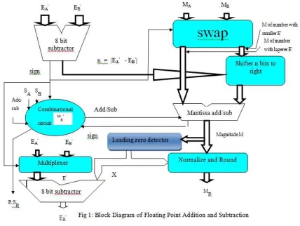
Fig 1: Block Diagram Of Floating Point Addition And Subtraction
2. FLOATING POINT
ADDITION/SUBTRACTION:
Using the Classic Timing Analyzer tool, it was observed that the new multiplier design using carry look ahead adder has less delay compared to the other
multiplier designs. The power consumption
calculations of the Floating Point
Addition/Subtraction were done successfully using
the paper comes up with a new multiplier design of less delay without compromising on the power consumption.[2]
The block diagram of 32-bit floating point addition/subtraction is as shown above
Steps in Floating point Addition/Subtraction Algorithm:
Step1:
(i) Read the two floating point numbers.
(ii)Subtract the exponents; if sign bit is 1 perform swapping operation between two mantissas otherwise no swapping.
(iii) The magnitude of exponent subtraction is used to shift the mantissa with lower exponent.
Step 2:
(i)This step is performed by 2:1 multiplexer
(ii)The result of mux is exponent A, if sign bit=0 or exponent B if sign bit=1.This sign bit is obtained from Step1
Step 3:
(i)The important block of addition subtraction algorithm is Combinational Control Network.
(ii)This Network determines which operation has to be performed on the two mantissas
(iii)Depending on two operand sign bits and add/subtract we can perform different operations for different combination of inputs
Step 4:
[image:3.595.317.521.76.297.2]After performing add/subtract of two mantissas, normalize the result of mantissa and adjust the exponent.
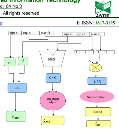
Fig 2: Flow Chart Representing The Floating Point Multiplier
Floating point Multiplication & Division:
Floating point multiplication process is much simpler process compared to addition and subtraction.
Floating Point Multiplication Algorithm:
i. First compute the sign, exponent, mantissa of the two operands.
ii. The sign bit of the result is obtained by xoring the sign bits of two operands.
iii. First convert the biased exponents to unbiased notation, add the exponents and then result of the exponent should be represented in biased notation. iv. Multiply the mantissas of two operands and this
result should be normalized that means the mantissa result should be in the range of [1,4).
v. The result is normalized by shift left, right correspondingly exponent was adjusted.
vi. After the normalization result is rounded to nearest value.
Rounding:
If we multiply the two twenty four bit operands then the result should be forty eight bits. So we have to discard extra bits and consider the result in twenty eight bit format. This process is done using Rounding.
1. 11011010001101010010110 GRS
We consider three extra bits these are
G(guard),R(round),S(sticky).
Floating point division Algorithm:
ii. Compute exponent of the result by subtracting the exponents of two operands and the result is biased. iii. In Non Restoring algorithm first load the register A
to zero, B with divisor and Q with dividend
The following loop executed ‘n’ number of times where n is number of dividend or divisor bits
i. Left shift operation is performed on A and Q ii. If sign bit of A is zero left shift A and Q,subtract A
and M and result is stored in A.and LSB of Q is set to 1.
iii. If sign bit of A is one left shift A and Q,add A and M and result is stored in A.and LSB of Q is set to 0. After executing these statements
If sign bit of A is Zero operation ends otherwise add A and M.
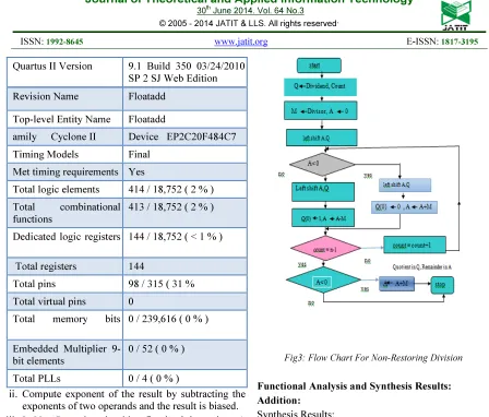
Fig3: Flow Chart For Non-Restoring Division
Functional Analysis and Synthesis Results: Addition:
Synthesis Results:
Subtraction:
Synthesis results:
[image:4.595.76.524.77.459.2]Fig 3: Functional Verification Of Adder
Quartus II Version 9.1 Build 350 03/24/2010
SP 2 SJ Web Edition
Revision Name Floatadd
Top-level Entity Name Floatadd
amily Cyclone II Device EP2C20F484C7
Timing Models Final
Met timing requirements Yes
Total logic elements 414 / 18,752 ( 2 % )
Total combinational functions
413 / 18,752 ( 2 % )
Dedicated logic registers 144 / 18,752 ( < 1 % )
Total registers 144
Total pins 98 / 315 ( 31 %
Total virtual pins 0
Total memory bits 0 / 239,616 ( 0 % )
Embedded Multiplier 9-bit elements
0 / 52 ( 0 % )
Fig 4: Functional Verification Of Subtraction
Multiplication: Synthesis results:
Quartus II Version 9.1 Build 350
03/24/2010 SP 2 SJ Web Edition
Revision Name Multiply
Top-level Entity Name Multiply
Family Cyclone II
Device EP2C20F484C7
Timing Models Final
Met timing requirements Yes
Total logic elements 127 / 18,752 ( < 1 % )
Total combinational
functions
127 / 18,752 ( < 1 % )
Dedicated logic registers 32 / 18,752 ( < 1 % )
Total registers 32
Total pins 97 / 315 ( 31 % )
Total virtual pins 0
Total memory bits 0 / 239,616 ( 0 % )
Embedded Multiplier 9-bit elements
7 / 52 ( 13 % )
Total PLLs 0 / 4 ( 0 % )
Fig 5: Functional Verification Of Multiplication
Quartus II Version 9.1 Build 350 03/24/2010
SP 2 SJ Web Edition
Revision Name Floatadd
Top-level Entity Name Floatadd
Family Cyclone II
Device EP2C20F484C7
Timing Models Final
Met timing requirements No
Total logic elements 414 / 18,752 ( 2 % )
Total combinational
functions
409 / 18,752 ( 2 % )
Dedicated logic registers 144 / 18,752 ( < 1 % )
Total registers 144
Total pins 98 / 315 ( 31 % )
Total virtual pins 0
Total memory bits 0 / 239,616 ( 0 % )
Embedded Multiplier 9-bit elements
0 / 52 ( 0 % )
Division:
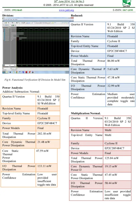
Fig 6: Functional Verification Of Division In Model Sim
Power Analysis:
Addition/ Subtraction: Normal:
Quartus II Version 9.1 Build 350
03/24/2010 SP 2 SJ WebEdition
Revision Name Floatadd
Top-level Entity Name Floatadd
Family Cyclone II
Device EP2C20F484C7
Power Models Final
Total Thermal Power
Dissipation
202.18 mW
Core Dynamic Thermal Power Dissipation
21.48 mW
Core Static Thermal Power Dissipation
47.59 mW
I/O Thermal Power
Dissipation
133.11 mW
Power Estimation
Confidence
Low user
provided insufficient toggle rate data
Reduced:
Quartus II Version 9.1 Build 350
03/24/2010 SP 2 SJ Web Edition
Revision Name Floatadd
Family Cyclone II
Top-level Entity Name Floatadd
Device EP2C20F484C7
Power Models Final
Total Thermal Power
Dissipation
86.00 mW
Core Dynamic Thermal P Dissipation
5.63 mW
Core Static Thermal Power Dissipation
47.38 mW
I/O Thermal Power
Dissipation
32.99 mW
Power Estimation
Confidence
Medium user
provided moderately complete toggle rate data
Multiplication:Normal.
Quartus II Version 9.1 Build 350
03/24/2010 SP 2 SJ Web Edition
Revision Name Multi
Top-level Entity Name Multi
Family Cyclone II
Device EP2C20F484C7
Power Models Final
Total Thermal Power
Dissipation
125.04 mW
Core Dynamic Thermal Power D
19.15 mW
Core Static Thermal
Power Dissipation
47.45 mW
I/O Thermal Power
Dissipation
58.44 mW
Power Estimation
Confidence
Low: user provided
insufficient toggle
Reduced:
Quartus II Version 9.1 Build 350
03/24/2010 SP 2 SJ Web Edition
Revision Name Multi
Top-level Entity Name Multi
Family Cyclone II
Device EP2C20F484C7
Power Models Final
Total Thermal Power
Dissipation
94.45 mW
Core Dynamic Thermal PD 5.83 mW
Core Static Thermal Power Dissipation
47.40 mW
I/O Thermal Power
Dissipation
41.22 mW
Power Estimation
Confidence
Medium: user
provided moderately
complete toggle
rate data
3. CONCLUSION:
All the Floating Point ALU modules are designed from block diagram approach and we performed synthesis, functional verification and power analysis for addition, subtraction and multiplication in Quartus II Altera and functional simulation for division in Model Sim. Here we have designed floating point ALU for normalized inputs; This ALU can also be extended for performing Square root, exponential and logarithmic. Even pipelining for above FPU can increase the efficiency. In order to increase the accuracy of mantissa we can implement it using IEEE 754 Double Precision Format.
Based on figure 1 to figure 6, the Functional Verification of various functions of ALU in ModelSim, Proposed Multiplication takes 25% less total thermal power dissipation, 88% less core dynamic thermal power dissipation and 30 % less I/O thermal power dissipation. Proposed Adder/Subtractor takes 57% less total thermal power dissipation, 45 % less core static thermal power dissipation, 73% less core dynamic thermal power dissipation and 75 % less I/O thermal power dissipation as per the above results developed by Quartus II Version 9.1 Build 350
03/24/2010 SP 2 SJ Web Edition for Cyclone II EP2C20F484C7.
REFRENCES:
[1] R. Zimmerman, “Efficient VLSI Implementation of Modulo 2n+1Þ Addition and Multiplication,” Proc. 14th IEEE Symp. Computer Arithmetic, pp. 158-167, Apr. 1999.
[2] H.T. Vergos, C. Efstathiou, and D. Nikolos, “Diminished-One Modulo 2n+1 Adder Design,” IEEE Trans. Computers, vol. 51, no. 12, pp. 1389-1399, Dec. 2002.
[3] H.T. Vergos and C. Efstathiou, “Efficient Modulo 2n + 1 Adder Architectures,” Integration, the VLSI J., vol. 42, no. 2, pp. 149-157, Feb. 2009. [4] H.T. Vergos, G. Dimitrakopoulos, On modulo 2n
+ 1 adder design, IEEE Trans. Comput. 61 (2) (2012) 173–186.
[5] S.-H. Lin and M.-H. Sheu, “VLSI Design of Diminished-One Modulo 2n + 1 Adder Using Circular Carry Section,” IEEE Trans. Circuits and Systems II, vol. 55, no. 9, pp. 897-901, Sept. 2008.
[6] Dhanabal R,,Bharathi V,Saira Salim, Bincy Thomas, Hyma Soman, Dr Sarat Kumar Sahoo “DESIGN OF 16-BIT LOW POWER ALU - DBGPU “ ,International Journal of Engineering and Technology (IJET) 2013.
[7] R Dhanabal,V Bharathi, Anand N, George Joseph, Suwin Sam Oommen, Dr Sarat Kumar Sahoo ,"Comparison of Existing Multipliers and Proposal of a New Design for Optimized
Performance " ,International Journal of
Engineering and Technology (IJET) 2013. [8] R Dhanabal, Ushashree, " Implementation of a