University of Windsor University of Windsor
Scholarship at UWindsor
Scholarship at UWindsor
Electronic Theses and Dissertations Theses, Dissertations, and Major Papers
2014
Modern Applications of Novel Electroless Plating Techniques
Modern Applications of Novel Electroless Plating Techniques
Robert Andrew Petro University of Windsor
Follow this and additional works at: https://scholar.uwindsor.ca/etd
Recommended Citation Recommended Citation
Petro, Robert Andrew, "Modern Applications of Novel Electroless Plating Techniques" (2014). Electronic Theses and Dissertations. 5095.
https://scholar.uwindsor.ca/etd/5095
This online database contains the full-text of PhD dissertations and Masters’ theses of University of Windsor students from 1954 forward. These documents are made available for personal study and research purposes only, in accordance with the Canadian Copyright Act and the Creative Commons license—CC BY-NC-ND (Attribution, Non-Commercial, No Derivative Works). Under this license, works must always be attributed to the copyright holder (original author), cannot be used for any commercial purposes, and may not be altered. Any other use would require the permission of the copyright holder. Students may inquire about withdrawing their dissertation and/or thesis from this database. For additional inquiries, please contact the repository administrator via email
Modern Applications of Novel
Electroless Plating Techniques
by
Robert Andrew Petro
A Dissertation
Submitted to the Faculty of Graduate Studies
through the Department of Physics
in Partial Fulfillment of the Requirements for
the Degree of Doctor of Philosophy at the
University of Windsor
Windsor, Ontario, Canada
2014
Modern Applications of Novel Electroless Plating Techniques
by Robert Petro
APPROVED BY:
___________________________ S. Mittler, External Examiner
Western University
___________________________ A. T. Alpas
Department of Mechanical, Automotive & Materials Engineering
___________________________ C. Rangan
Department of Physics
___________________________ J. W. McConkey
Department of Physics
___________________________ M. Schlesinger, Advisor
Department of Physics
Declaration of Co-Authorship / Previous Publication
I. Co-Authorship Declaration
I hereby declare that this dissertation incorporates material that is result of joint
research, as follows:
This dissertation incorporates the outcome of a joint research undertaken with, and under, the supervision of Dr. M. Schlesinger. The collaboration is covered in Chapters 3, 4, and 5 of the dissertation. In all cases, the key ideas, primary contributions, experimental designs, data analysis, and interpretation, were performed by the author.
I am aware of the University of Windsor Senate Policy on Authorship and I certify that I have properly acknowledged the contribution of other researchers to my dissertation, and have obtained written permission from each of the co-author(s) to include the above material(s) in my dissertation.
I certify that, with the above qualification, this dissertation, and the research to which it refers, is the product of my own work.
II. Declaration of Previous Publication
This dissertation includes four (4) original papers and that have been previously published/submitted for publication in peer reviewed journals, as follows:
Dissertation
Chapter Publication Title/Full Citation
Publication Status
Chapter 3 R. Petro and M. Schlesinger, “Direct Electroless
Deposition of Nickel Boron Alloys and Copper on Aluminum Containing Magnesium Alloys”,
Electrochemical and Solid-State Letters, 14, (2011), p.D37-D40
Published
Chapter 3 R. Petro and M. Schlesinger, “Direct Electroless
Deposition of Low Phosphorous Ni-P Films on AZ91D Mg Alloy”, Journal of The Electrochemical Society, 159, (2012), p.D455-D461
Published
Chapter 3 R. Petro and M. Schlesinger, “Direct Electroless
Deposition of Ni-P-Zn Films on AZ91D Mg Alloy”, Journal of The Electrochemical Society, 160(9), (2013), p.349-353
Published
Chapter 3 M. Schlesinger and R. Petro, “Process for Electroless
Deposition on Magnesium Using a Nickel Hydrate
Plating Bath ”, Date Filed: February 14th 2013 Patent #:
US 20130216721
Chapter 3 & Chapter 4
M. SchlesingerandR. Petro, “Process Patent for
Electroless Deposition of Metals using Highly Alkaline Plating Bath”, International filing date under PCT (Patent Cooperation Treaty): October 12, 2011; Issued: August 15, 2013, Serial number: CA2011/001146, Patent #:US 20130209698
Patent Issued
Chapter 4 M. SchlesingerandR. Petro “Process for Electroless
Deposition of Gold and Cu Alloys on Silicon” (2013)*
Patent Filed
Chapter 5 M. Schlesinger and R. Petro “Electro-Electroless Hybrid
Multi-layer and Alloy Deposition” (2014)*
Patent Filed
Chapter 5 R. Petro and M. Schlesinger, “Development of Novel
Hybrid Electro-Electroless Deposit (HEED) Coatings and Applications”, (2014) Submitted for Publication Chapter 2.4 & Chapter 3.1
R. Petro and M. Schlesinger, Chapter 1: Applications of Electrochemistry in Medicine, in “Modern Aspects of Electrochemistry Vol:56 - Applications of
Electrochemistry in Medicine”, p.1-32, ed. M.
Schlesinger, (2013), Springer Science+Business Media New York, ISBN 978-1-4614-6148-7
Published
Chapter 2.1 &
Chapter 7.4
R. Petro, M. Schlesinger, and G.-L. Song; Chapter 30: Ionic Liquid Treatments for Enhanced Corrosion
Resistance of Magnesium-Based Substrates, in “Modern Electroplating, Fifth Edition”, p.665-686, eds: M.
Schlesinger and M. Paunovic, (2010) John Wiley & Sons, Inc., Hoboken, NJ, USA.
doi:10.1002/9780470602638.ch30
Published
*Exact Tiles Unavailable
I certify that I have obtained a written permission from the copyright owner(s) to include the above published material(s) in my dissertation. I certify that the above material describes work completed during my registration as graduate student at the University of Windsor.
I declare that, to the best of my knowledge, my dissertation does not infringe upon anyone’s copyright nor violate any proprietary rights and that any ideas, techniques, quotations, or any other material from the work of other people included in my dissertation, published or otherwise, are fully acknowledged in accordance with the standard referencing practices. Furthermore, to the extent that I have included copyrighted material that surpasses the bounds of fair dealing within the meaning of the Canada Copyright Act, I certify that I have obtained a written permission from the copyright owner(s) to include such material(s) in my dissertation.
Abstract
This dissertation is composed of three distinct but closely related topics on the
electrochemical metallization of substrates. The first topic solves the longstanding
problem of galvanic corrosion in connection with exploiting the advantageous properties
of magnesium {Mg} alloys and is of vital interest to the automotive and aerospace
sectors. The second topic provides a new approach to the selective electroless
metallization of silicon {Si} in connection with solar cells and other electronic devices.
The third topic details a novel method of metal thin film formation using wet chemistry
techniques which allow for the deposition of alternating metal layers of different and
similar nobility from a single electrolyte. Future possible avenues of investigation are
suggested for each of the three topics. The resolution of the galvanic corrosion issue, as
presented within herein, is based on the direct electroless deposition of metal thin films
less active than the Mg alloy substrates. Claddings of copper {Cu}, nickel boron {Ni-B},
and phosphorous {P} alloys including: nickel {Ni-P}, cobalt {Co-P}, nickel-zinc
{Ni-Zn-P}, and other ternary alloys, were successfully deposited directly on Mg alloy
surfaces. The electroless coating of Mg alloys was accomplished using minimal
pre-treatments and made use of the naturally active properties of Mg-based substrates.
Qualitative measures of the corrosion resistance of Ni-Zn-P coatings on Mg alloys
demonstrated superior resistance to galvanic corrosion compared to uncoated surfaces.
The selective electroless metallization of Si is accomplished with the selective removal of
the silicon oxide {SiOx} by means of mechanical scribing thereby exposing Si. The
exposure of Si provides a catalytic surface for the electroless deposition of gold {Au},
and silver {Ag}, and other metals. The mechanical scribing provides an inexpensive
avenue for the selective metallization of Si for solar cells. The novel method of
depositing alternating metal layers of both different and similar nobility is achieved by
combining electroplating and electroless deposition within a single electrolyte. The
technique, termed here “hybrid electro-electroless deposition” (HEED), provides coatings
previously unobtainable using wet electrochemical techniques. The application of HEED
is of interest for the provision of sacrificial coatings on Mg alloys for corrosion protection
Acknowledgements
The work contained within this dissertation would not have possible if not for the
help and support of a number of individuals. Most importantly, I would like to thank
Dr. Mordechay Schlesinger for accepting me as his Masters level graduate student and
encouraging me to pursue my Doctorate degree of which this dissertation is part.
Without his guidance none of the work in this dissertation would have been possible, and
I am grateful for his trust and belief in my abilities. Additionally, I would also like to
thank the folks at GM, especially Dr. Mark Verbrugge, Dr. Jan Herbst, and Dr. Justin
Gammage, as well as Jose Costa from the Ontario Centers for Excellence.
I would like to thank the entire Faculty of the Department of Physics for the
quality education and guidance provided to me throughout my undergraduate degree and
graduate studies. I would like to gratefully acknowledge all University of Windsor staff
and in particular specifically thank: Physics Machine Shop Technicians Louis Beaudry
and Eric Claussen, for assisting in the production of substrates as well as providing
practical insight into the properties of metals; Computer and Electronics Technicians
Aldo DiCarlo and Senisa Jedzic, for both help with equipment as well as the procurement
thereof; secretaries Qin Tu, Sabina Baraoniciu, Martha Hiuser, and Kimberly Lefebvre,
who helped with the paperwork associated with being a graduate student; and SEM
Technicians Sharon Lackie and John Robinson for help with SEM and EDS analysis.
Additionally I thank the custodians of Essex hall, including Tom Dean and others, who
helped keep the lab clean and deal with messes cause by equipment failures.
I thank all graduate and undergraduate students for their friendship over the
course of this work. In particular I wish to thank Dr. Michael Sullivan, as well as Nissa
Frank and Michael Bolla, who, as graduate students along with me, kept an open door
policy to talk about everything from research/academic pursuits to more social topics.
Finally, and most importantly, I would like to thank my mother, Emese, and my
brother, Nicholas, both of whom I can never thank enough for their support and love.
Without their support I would never have been capable of accomplishing the work within
this dissertation. To Jennifer Trymbulak, thank you for your support throughout my
Table of Contents
Declaration of Co-Authorship/Previous Publications iii
Abstract v
Dedication vi
Acknowledgements vii
List of Tables xii
List of Figures xv
Chapter 1: Introduction
11.1 Overview 2
1.2 Summary of Dissertation 3
1.3 History of Deposition 4
1.4 References 11
Chapter 2: Background
142.1 Introduction of Deposition Concepts and Properties 15
2.2 Electroplating & Electrochemistry 17
2.2.1 Electroplating Cell 18
2.2.2 Electroplating Conditions 21
2.2.3 Electroplating Techniques 28
2.2.4 Electroplated Films: Deposition & Structure 32
2.2.5 Selective Deposition 37
2.3 Electroless Deposition 41
2.3.1 Electrolyte Composition 42
2.3.2 Theoretical Considerations 52
2.3.3 Electroless Alloys & Composites 56
2.4 Single and Multi-layered Thin Film Deposit Properties 62
2.4.1 Diffusion & Deposit Brittleness 63
2.4.2 Multi-Layers 66
2.4.3 Hardness 68
2.4.4 Magnetic Properties & Giant Magneto-Resistance (GMR) 73
2.4.4.1 Magnetization & Coercivity of Thin Films 74
2.4.4.2 Fundamentals of Magneto-Resistance 76
2.4.4.3 Larger Magneto-Resistance Effects 82
2.5 Magnesium & Corrosion 87
2.5.1 Corrosion 89
2.5.2 Galvanic Corrosion 95
2.6 Summary 98
2.7 References 99
Chapter 3: Electroless Cladding of Magnesium {Mg}
1063.1 Introduction to Applications of Magnesium {Mg} 107
3.2 Current Anti-Corrosion Practises 107
3.3 Materials and Methodology 112
3.3.1 Sample Analysis 113
3.4 Results 114
3.4.1 Early Work 115
3.4.2 Electroless Copper {Cu} and Nickel Boron {Ni-B} 129
3.4.2.1 Surface Treatments 137
3.4.2.2 Immersion Coatings and Electrolyte Modifications 141
3.4.2.3 Metallic, Electroless Cu Coating of AZ91D Mg Alloys 160
3.4.3 Electroless Nickel Phosphorous {Ni-P} and Other Binary Alloys 162
3.4.4 Electroless Nickel-Zinc-Phosphorus {Ni-Zn-P} and Other Ternary Alloys
177
3.5 Summary 195
Chapter 4: Selective Electroless Deposition on Silicon {Si}
2014.1 Introduction to Selective Deposition on Silicon {Si} 202
4.2 Silicon Materials and Applications 202
4.3 Experimental Motivation 209
4.4 Materials and Methods 213
4.5 Experimental Results 214
4.5.1 Electroless Copper {Cu} 216
4.5.2 Electroless Gold {Au} 219
4.5.3 Electroless Nickel {Ni} 222
4.5.4 Role of Ammonium/Ammonia {NH4+/NH3} 227
4.5.5 Electroless Silver {Ag} 231
4.6 Summary 233
4.7 References 234
Chapter 5: Hybrid Electro-Electroless Deposition
239
5.1 Overview of Electroplating and Electroless Deposition 240
5.2 Theory 242
5.2.1 Multi-layer Deposition 243
5.2.2 Alloy Deposition 246
5.3 Materials and Methodology 246
5.3.1 Electroless Gold {Au} Electrolytes 247
5.3.2 Electrodes and Deposition System 248
5.3.3 Sample Analysis 250
5.4 Ni/Au and Co/Au Results 251
5.5 Application to Coatings on Mg Alloys 259
5.6 Iron Nickel {Fe/Ni} Electrolyte and Ongoing Work 262
5.7 Summary 271
Chapter 6: Summary
273
6.1 Overview of Summary 274
6.2 Magnesium {Mg} 274
6.3 Silicon {Si} 275
6.4 Hybrid Electro-Electroless Deposit (HEED) Coatings 276
Chapter 7: Future Work
278
7.1 Introduction of Future Work 279
7.2 Cladding of Magnesium {Mg} Alloys 279
7.3 Electroless Metallization of Silicon {Si} 280
7.4 Hybrid Electro-Electroless Deposition (HEED) Coatings 281
7.5 Ionic Liquids (ILs) 281
Appendix A: Summary of Electroless Electrolytes
283
A.1 Electroless Silver {Ag} 283
A.2 Electroless Gold {Au} 285
A.3 Electroless Copper {Cu} 291
A.4 Electroless Nickel Boron {Ni-B} Alloys 293
A.5 Electroless Nickel Phosphorus {Ni-P} Alloys 294
A.6 Electroless Nickel Zinc Phosphorus {Ni-Zn-P} Alloys 295
A.7 Electroless Cobalt Phosphorus {Co-P} Alloys 296
A.8 Other Electroless Nickel Metal Phosphorus {Ni-Me-P} Alloys 297
A.9 References 298
Appendix B: Nickel/Gold {Ni/Au} Electro-Electroless Layers
on a Cobalt {Co} Substrate
300
List of Tables
2.1 Selected half-reactions along with their standard electrode potential
relative to SHE 22
2.2 Crystal structure of commonly deposited metals. 37
2.3 Chemical dissociation reactions and pKa for select complexing agents. 45
2.4 Denticity and equilibrium constants for select complexing agent anions. 47
2.5 Effective pH range and oxidation potential of some Ni reducing agents. 53
2.6 Comparison of properties of selected Fe, Al, and Mg alloys, as well as
common pure Cu and Ni. 87
2.7 Select results of 2.5 year corrosion exposure tests on sheet alloys. 89
2.8 Comparison of spontaneity and stability for the corrosion of Mn in water
with, and without, dissolved oxygen. 91
2.9 Type, condition, composition, and tensile strength of select Mg alloys. 92
2.10 Select corrosion potentials of synthetically prepared intermetallic phases
a de-aerated, 5 % NaCl, saturated Mg(OH)2, pH 10.5, environment 93
2.11 Anodic Index 96
3.1 Nominal compositions of the AZ91D and AM50 Mg alloys by wt. % 112
3.2a Pre-treatment process by J. Marton and M. Schlesinger 116
3.2b Acidic electroless Ni-P electrolyte formulation by J. Marton and
M. Schlesinger 116
3.3 Stannate surface conversion treatment for Mg alloys as modified from
Huo et al. 117
3.4 Common alkaline Ni-P metallization electrolyte. 118
3.5 Electrolytes for the pre-treatment of AZ91D Mg alloy samples prior to
metallization from a Ni-B electrolyte. 119
3.6 Electroless Ni-B electrolyte formulation modified from Gorbunova et al. 120
3.7 Composition and operating conditions for the pre-treatment and
subsequent Ni-P and Ni-B metallization of Mg alloys. 122
3.8 Acidic HF and alkaline Zn surface pre-treatments for Mg alloys. 124
3.9 Electroless Cu thin film electrolytes. 129
3.10 Formulation for co-deposition of Co with Ni-B modified from Table 3.5. 133
3.11 Modified electroless Cu thin film electrolytes. 141
3.13 Likely half-reactions and associated standard electrode potentials for the
formation of Cu immersion coatings on Mg alloys. 153
3.14 Alkaline Cu electrolytes for immersion deposits on Mg alloys 154
3.15 Modified electroless Cu thin film electrolyte 161
3.16 Acidic Ni-P electrolyte, nearly identical to the electrolyte in Table 3.2. 162
3.17 Electroless Ni-P thin film electrolyte for successful deposition on Mg
alloys. 163
3.18 Formulations of successful electroless Ni-P thin film electrolytes for
deposition on Mg alloys. 165
3.19 Formulations of unsuccessful electroless Ni-P thin film electrolytes for
deposition on Mg alloys. 166
3.20 Alkaline electroless Co electrolyte 176
3.21 Alkaline electrolyte for the deposition of electroless Ni-Zn-P alloys on
Mg alloys. 177
3.22 Formulations of alkaline electrolytes for the deposition of various
electroless Ni-Zn-P alloys on Mg alloys. 180
3.23 Electrolyte for Ni-Zn-P immersion deposit 189
3.24 Alkaline electroless Ni-Co-P electrolyte 190
3.25 Alkaline electroless Ni-Fe-P electrolyte 192
3.26 Alkaline electroless Ni-Re-P and Ni-W-P electrolytes 193
3.27 Electrolyte compositions, and conditions, for electroless Ni-P, Ni-Zn-P,
and Ni-Co-P deposits on Mg alloys. 197
4.1 Composition of the electroless Cu electrolyte 216
4.2 Electroless Au electrolyte 219
4.3 Acidic and neutral electroless Ni-P electrolytes. 223
4.4 Electroless Ni-P electrolytes 227
4.5 Electroless Ag electrolyte 232
5.1 Summary of differences between electroplating and electroless plating 241
5.2 Electrolyte for electroless Ni-Fe-P alloy deposition 244
5.3 Electroless Au/Ni and Au/Co electrolytes for electro-electroless
deposition 248
5.4 Nominal composition of the Ni, Cu, and Co electrodes 249
5.6 Hybrid electro-electroless electrolyte, 3:1 Ni:Fe ratio, for Fe/Ni
deposition. 262
5.7 Measured voltage, current, and duration of electroplated Fe/Ni deposits
with atomic % and weight % EDS results for deposits at various applied voltages.
264
5.8 Standard electrode potentials for Ni and Fe metals 268
A1 Electroless Ag electrolytes 283
A2 Electroless Au electrolyte 285
A3 Electroless Cu thin film electrolytes 291
A4 Electroless Ni-B electrolyte 293
A5.1 Acidic electroless Ni-P electrolyte 294
A5.2 Alkaline electroless Ni-P electrolyte 294
A6 Electroless Ni-Zn-P electrolytes 295
A7 Electroless Co-P and Ni-Co-P electrolytes 296
List of Figures
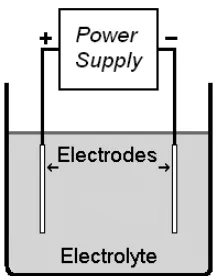
2.1 Schematic of the basic arrangement of an electroplating cell 17
2.2 Schematic of electroplating cell with reactions for nickel deposition 20
2.3 Typical voltammetric curves for two different metals, M1 & M2. 29
2.4 Ion transfer to a terrace site, surface diffusion, and incorporation at
kink site. 34
2.5 Schematic representation of layer growth and the nucleation–
coalescence mechanism. 35
2.6 Unit cells of the three crystal lattices of commonly deposited
metals. 37
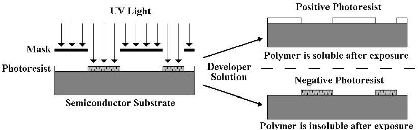
2.7 Insoluble/soluble (positive/negative) photoresists rendered
soluble/insoluble to a developer solution after UV light exposure. 38
2.8 Schematic of the Rayleigh Criterion for resolvability. 39
2.9 Evans type mixed potential diagram for the reduction of Cu2+ ions,
and for oxidation of formaldehyde reducing agent. 55
2.10 Wagner-Traud type mixed potential diagram for electroless Ni-B
deposition 56
2.11 Hardness data for electrochemically grown Cu/Ni super-lattice
multi-layers 71
2.12 Schematic of hysteresis loops 76
2.13 Schematic magnetization versus applied magnetic field 76
2.14 Spin polarization for paramagnetic and ferromagnetic materials 78
2.15 Schematic of the anisotropic magneto-resistance (AMR) effect 80
2.16 Diagram of the Hall Effect and resulting forces on an electron
within a conducting metal 81
2.17 Schematic of the idealized magnetization of the super-lattice in
multi-layers producing the GMR effect 83
2.18 Superposition of all contributions toward observed GMR. 84
2.19 Examples of the dependence of spacer layer thickness, Cu, on GMR
at magnetic saturation for Ni-Cu and Co-Cu multi-layers. 85
2.20 Die cast AZ91D salt spray performance versus Fe, Ni, and Cu
tramp element content. 94
3.1 Incremental and 30 minute immersion deposits of Ni-P deposit from
an acidic electrolyte on AZ91D Mg alloy with stannate surface conversion.
3.2 Electroless Ni-B “Hulk” coating of an AZ91D Mg alloy substrate. 120
3.3 Comparison of electroless Ni-B coatings on fly-cut AZ91D Mg
alloys with 25 °C acidic pre-treatment and alkaline 90 °C stannate conversion treatments
121
3.4 Electroless Ni-P metallization of fly-cut AM50 and AZ91D Mg
alloys samples after acidic Mn-cocktail pre-treatment. 123
3.5 Comparison of Ni-P deposits from electrolytes of varying
concentrations of thiourea SC(NH2)2 and HF.
124
3.6 Magnification (10×) of HF and acidic Mn-cocktail pre-treated
AZ91D Mg alloy surfaces. 125
3.7 Comparison of Ni-P metallization of fly-cut, acidic Mn-cocktail and
HF pre-treated AZ91D Mg alloy samples. 125
3.8 Electroless Ni-P coating on fly-cut AZ91D Mg alloys from
HF-containing and HF-free Ni-P electrolytes. 126
3.9 Comparison of electroless Ni-P deposits from an HF-containing
electrolyte on Zn treated Mg alloys. 127
3.10 Macroscopic, backscatter SEM, and EDS analysis comparison of electroless deposits formed by alkaline Cu electrolytes on oxidized and polished AZ91D Mg alloy substrates.
131
3.11 Macroscopic scan, backscatter SEM image, and EDS analysis of a
Ni-B coated AZ91D substrate. 132
3.12 Macroscopic scan, backscatter SEM image, and EDS analysis of an
AZ91D substrate coated with a Co doped Ni-B layer. 133
3.13 Macroscopic scan, backscatter SEM image, and EDS analysis for AM50 and AZ91D samples coated with an initial Ni-B layer and subsequent Cu layer
134
3.14 Macroscopic scanned image accompanied by EDS analysis and backscatter SEM images of an AZ91D sample having initial Ni-B layer and secondary Cu layer deposits.
136
3.15 Macroscopic scanned images of a stannate treated AZ91D samples
with and without an electroless Cu deposit. 138
3.16 Macroscopic images of electroless Cu deposits on concentrated
HNO3 and dilute H2SO4 acid pre-treated Mg alloy samples.
138
3.17 Macroscopic images, and negatives, comparing the post-tape test
surfaces of Cu deposits on stannate conversion, H2SO4 etched, and
polished AZ91D Mg alloy samples.
140
3.18 Macroscopic and backscatter SEM image of a Cu immersion
3.19 Macroscopic images of 48 hour Cu immersion deposits on AZ91D Mg alloys within electrolytes of varying NaOH concentration, < 15 g/L.
144-145
3.20 Macroscopic images of 48 hour Cu immersion deposits on AZ91D Mg alloys within electrolytes of varying NaOH concentrations,
≥ 15 g/L. 146-147
3.21 Backscatter SEM images of immersion Cu coatings formed on
AZ91D Mg alloys at pH 11.5 and 12.7. 148
3.22 Titration curve for the alkaline Cu electrolyte. 148
3.23 Titration curves for the alkaline Cu electrolytes containing differing
concentrations of CuSO4∙ 5H2O.
149
3.24 Titration curve for the alkaline Cu immersion electrolyte showing
the pH of the electrolyte after 96 hours. 150
3.25 Macroscopic scanned image of the large faces of a polished AZ91D
Mg alloy sample after 40hrs immersion in a pH 11.6 Cu electrolyte. 151
3.26 Compositional EDS analysis of oxide/hydroxide crystallites on the reverse of the Cu film formed on AZ91D Mg from a pH 10.5 Cu electrolyte.
152
3.27 Compositional EDS analysis of the shed Cu thin film produced on
AZ91D Mg from a pH 11.5 Cu electrolyte. 153
3.28 Macroscopic image of 14 h Cu immersion deposits on the polished
and oxidized sides of AZ91D Mg alloys. 155
3.29 Backscatter SEM images comparing Cu immersion deposits formed on AZ91D Mg alloys within electrolytes containing varying
concentrations NH4OH.
156
3.30 Macroscopic image along with backscatter SEM image of a Cu immersion coatings formed on an AZ91D Mg alloys within an
electrolyte containing 83.3 mL/L NH4OH.
157
3.31 Macroscopic scans of 23 h and 68 h deposits on Sn/Pd treated glass
from a Cu immersion electrolyte containing MgSO4.
157
3.32 Backscatter SEM images and EDS of a 68 h deposit on Sn/Pd
treated glass from a Cu immersion electrolyte containing MgSO4. 158
3.33 Macroscopic scanned images of an electroless Cu deposit on a dry
polished AZ91D Mg alloy. 160
3.34 Macroscopic image, backscatter SEM images and EDS analyses of
an acidic electroless Ni-P coating on an AZ91D Mg alloy. 163
3.35 Macroscopic image, backscatter SEM images, and EDS analyses of
3.36 Macroscopic scan, backscatter SEM image, and EDS analyses of an
alkaline electroless Ni-P deposit from Bath F3, containing Cl– ions,
on a dry polished AZ91D Mg alloy.
167
3.37 Macroscopic scan, backscatter SEM image, and EDS analysis of an alkaline electroless Ni-P deposit, from Bath S2, on dry a polished AZ91D Mg alloy.
168
3.38 Macroscopic scan, backscatter SEM image, and EDS analyses of an alkaline electroless Ni-P deposit, from Bath S4, on a dry polished AZ91D Mg alloy.
168
3.39 Macroscopic scans of failed deposits from Baths F4 and F5 on
AZ91D Mg alloys. 169
3.40 Backscatter SEM images and EDS analyses of an oxidized AZ91D
Mg alloy sample with No, 2 min, and 5 min deposits from Bath S6. 171
3.41 Macroscopic scans, backscatter SEM images, and EDS analyses, of
a Ni immersion deposit formed on a AZ91D Mg alloy. 174
3.42 Macroscopic image, SEM image, and EDS analysis of an
electroless Co-P thin film on a polished AZ91D Mg alloy. 176
3.43 Macroscopic scan, backscatter SEM image, and EDS analyses of a
Ni-Zn-P on a polished AZ91D Mg alloy. 178
3.44 Macroscopic scan, backscatter SEM image, and EDS analysis of a
Ni-Zn-P deposit on an oxidized AZ91D Mg alloy. 179
3.45 Backscatter SEM images and EDS analyses of Ni-Zn-P deposits, on oxidized AZ91D Mg alloys, from electrolytes containing various relative concentration of Ni2+/Zn2+.
182
3.46 Macroscopic scans, backscatter SEM images, and EDS analyses of Ni-Zn-P deposits, of different duration, from electrolytes containing 25 % mol Zn on oxidized AZ91D Mg alloys.
184
3.47 Macroscopic scans, and negatives, of pre-, and post-, galvanic
coupling of uncoated and Ni-Zn-P coated AZ91D Mg alloys. 186
3.48 Macroscopic scan, SEM image, EDS analysis of a Ni-Zn-P deposit,
containing high P, on an AZ91D Mg alloy. 188
3.49 SEM image and EDS results for Ni-Zn-P immersion deposit on
AZ91D Mg alloy 189
3.50 Macroscopic scan, SEM image, EDS analysis of a Ni-Co-P deposit
on an AZ91D Mg alloy. 191
3.51 Macroscopic scan image of a shedding Ni-Co-P deposit on an
3.52 Backscatter SEM image and associated EDS of a Ni-Fe-P deposit
on an AZ91D Mg alloy. 192
3.53 Backscatter SEM images and associated EDS of a Ni-Re-P deposit
on an oxidized AZ91D Mg alloy. 194
4.1 Schematic crystal structure of n-type and p-type Si. 203
4.2 Schematics of the band structure of n-type, intrinsic, and p-type
semiconductors. 204
4.3 Band structure change within a junction transistor after the
application of a potential across the transistor. 206
4.4 Schematic diagram of a solar cell. 207
4.5 SEM images of the micro-textured pattern on p-type and n-type Si
wafers used. 213
4.6 Macroscopic image, backscatter SEM images, and EDS analyses of
selective electroless deposits of Cu on n-type Si. 217
4.7 Backscatter SEM image and EDS analysis of an attempted
electroless deposit of Cu on n-type Si from an electrolyte containing no reducing agent.
218
4.8 Macroscopic, backscatter SEM, and EDS comparison of electroless
Au deposits on n-type silicon formed from pH 7 and pH 10 electrolytes not containing Na3C6H5O7.
220
4.9 Backscatter and secondary emission SEM images, along with
associated EDS of electroless Au deposits on n-type and p-type Si formed under differing conditions.
222
4.10 Macroscopic image, backscatter SEM image, and EDS analysis
20min acidic electroless Ni-P deposits on n-type Si. 223
4.11 Macroscopic image, secondary emission SEM images, and backscatter SEM image, with EDS analysis, of a Ni-P cluster on scribed Si.
225
4.12 Comparison of macroscopic images and microscopic optical images
of the Ni-P deposits on scribed n-type Si wafers. 226
4.13 Macroscopic scanned images of polished and textured Si surfaces, along with backscatter SEM images, and associated EDS analysis of n-type Si surface post immersion in Ni immersion electrolytes with different pH adjusting chemicals.
228
4.14 Macroscopic scan comparison of the polished and textured sides of
control and post- alkaline Ni immersion n-type Si wafers. 229
4.15 Backscatter SEM images of Co precipitates/crystallites formed on
4.16 Macroscopic image, backscatter SEM image, and EDS analysis of a
selective electroless Ag deposit on n-type Si. 232
5.1 Schematic diagram of the electro-electroless plating system. 249
5.2 Macroscopic image of electroless/electro/electroless tri-layer
20 min-Au/60 s-Co/20 min-Au deposit, from a pH 7 electrolyte, on a Ni plate, along with sequential backscatter SEM images and EDS analysis of each layer.
252
5.3 Graph of EDS results for a sequential analysis of the tri-layer
deposit presented in Figure 5.2. 253
5.4 Graph of EDS results of a sequential 20 min-Au/60 s-Co/20 min-Au
tri-layer deposits on Ni from a pH 10 electrolyte. 254
5.5 Macroscopic image, with backscatter SEM images of a Co/Au
tri-layer HEED coating 5 min-Au/60 s-Co/5 min-Au on a Ni substrate, including a graph of sequential EDS analysis of the surface layers.
256
5.6 Macroscopic images, backscatter SEM images, and a graph of EDS
analysis electroplated Co on Ni from an 80 °C Co/Au HEED electrolyte for three different applied potentials.
257
5.7 Macroscopic images, backscatter SEM images, and EDS for
electroplated Ni on Co from an 80 °C Ni/Au HEED electrolyte for two different applied potentials.
258
5.8 Poor-man (PM) voltammogram for the alkaline Co/Au electrolyte. 259
5.9 Backscatter SEM image and associated EDS analysis of a
Ni-Zn-P/Ni-Zn HEED coating on an AZ91D Mg alloy. 261
5.10 Macroscopic image, backscatter SEM image, and EDS analysis of an electroless Ni-P deposit from a 3:1 Ni:Fe electrolyte on Sn/Pd treated glass.
263
5.11 Plot of the measured voltage and current for an applied deposition potential of 2.5 V for the deposition of Fe from a 3:1 Ni:Fe
electrolyte.
264
5.12 Plot of the atomic % of Ni, Fe, and P within the electroplated
coatings presented in Table 5.7. 265
5.13 Macroscopic scan, backscatter SEM images, and EDS analyses for an electroplated, 5 V applied, Fe/Ni deposit on a Cu substrate from a newer Fe/Ni electrolyte.
266
5.14 Macroscopic scan, backscatter SEM images, and EDS analyses for an electroplated, 4.6 V applied, Fe/Ni deposit on a Cu substrate from a newer Fe/Ni electrolyte.
5.15 Macroscopic scan, backscatter SEM images, and EDS analyses for an electroplated, 5 V applied, Fe/Ni deposit on a Cu substrate from an older Fe/Ni electrolyte.
267
5.16 Macroscopic scan, backscatter SEM images, and EDS analysis of a
Fe/Ni HEED bi-layer deposit from a newer Fe/Ni electrolyte. 269
5.17 Macroscopic scan, backscatter SEM images, and EDS analysis of a
Fe/Ni HEED bi-layer deposit from an older Fe/Ni electrolyte. 270
A1 Macroscopic scanned image, backscatter SEM image, and EDS
analysis of an Au deposit on a Cu substrate. 288
A2 Backscatter SEM image with EDS analysis of a Cu containing Au
deposit on a Co substrate. 289
B1 Macroscopic image along with a graph of EDS results for a Ni/Au
Chapter 1: Introduction
1
1.1 Overview 2
1.2 Summary of Dissertation 3
1.3 History of Deposition 4
1.1 Overview
The metallic coating of surfaces is a practise which has evolved over the course of
the 20th century from an art to an exact science. Historically, coatings have been
achieved by many different means including mechanical application; electrochemical
plating techniques such as electroplating and electroless plating; vacuum depositions
including chemical vapour deposition (CVD), and physical vapour deposition
(PVD)/sputtering techniques; chemical conversion techniques such as anodizing; and
spray coatings. Beyond improving the aesthetic appearance of surfaces with the
deposition of gold, chrome, or other metals; surface coatings play an integral role in an
ever-increasing number of applications in science and engineering.
Electroplating, the most widely used modern method for applying coatings, is a
practical branch of electrochemistry, which itself is often classified as a branch of
chemistry. Electrochemistry, of which electroplating, electroless plating, and anodizing
are parts, is the study of reactions involving electron transfer processes in conductive
solutions, known as electrolytes, between ionic species in solution and submerged
electron conductors, such as metals or semiconductors. Given the use of solutions in
electrochemistry, the term wet chemistry is often used signifying chemistry carried out in
the liquid phase. Despite the basis in chemistry, electrochemistry, including
electrochemical processes and products such as electrochemical deposition, exists as a
multidisciplinary science involving chemistry, engineering, biology, and, most
fundamentally, physics.
Electroplating, as well as electroless plating, constitute an essential component for
all aspects of electronics, both macro- and microscopic, and play a vital role in key
sectors such as transportation, specifically within the automotive industry, where coatings
are applied for wear corrosion resistance and aesthetic purposes. Both electro- and
electroless methods of depositing metallic thin films have advantages and disadvantages
compared to each other with each fulfilling specific purposes. Electroforming, an
application of electroplating, is the deposition of a metal film onto a surface such that
once the deposit is removed from the surface to form a free standing object which can
hobbyists for decorative plating purposes. Electroless plating, the chemical reduction of
metal ions to metallic form, is another means of metal film deposition that possesses the
often cited advantages of the ability to deposit on non-conducting surfaces of complex
shape. Electroplating requires a conductive surface upon which deposition occurs, and
uniform deposition using electroplating is not possible as a deposition is dictated by
electric field lines in a line of sight manner.
Research into electro- and electroless plating baths and techniques, as well as the
properties of resulting coatings is of ongoing interest throughout the academic and
industrial settings. This dissertation presents, among a number of topics, new and
patented developments in: the application of electrolessly deposited, galvanic corrosion
resistant claddings on magnesium alloys, some results of which have been previously
published [1-6]; the electroless deposition of conductive metals directly on silicon wafers
[4]; as well as a hybridized method for multi-layer and customized thin film alloy
deposition using a combination electro/electroless plating technique within a single
electrolytic deposition bath [6]. The hybrid deposition technique delineated within this
dissertation provides a novel method for the deposition of multi-layers of metal pairs
previously unavailable using wet chemistry, and previously only available by means of
molecular beam epitaxy [7], sputtering [7, 8], or other vacuum deposition techniques.
1.2 Summary of Dissertation
The remainder of this Chapter, Chapter 1, covers the history of deposition
focusing on the historical development of electro- and electroless plating throughout the
19th and 20th centuries. The contents of Chapter 2 provide the scientific background and
considerations as well as applications of electro- and electroless plating. The first two
sections of Chapter 2 focus on the electrochemistry of electroplating, Section 2.2, and
electroless deposition, Section 2.3, while the latter sections focus on more practical
applications. Specifically, the deposition and properties of multi-layers, produced
primarily by electroplating means, Section 2.4, and properties and corrosion of
magnesium alloys, Section 2.5, provide relevant modern applications of electroplating
and electroless deposition. Readers interested in the electroless deposition of metals on
for the understanding of hybrid deposition is covered in Sections 2.2 & 2.3, while readers
interested in the specific applications of hybrid multi-layer deposits are encouraged to
include Section 2.4.
The experimental sections of Chapter 3 & 4 contain the background, theory,
results, and current status of electroless deposition on Mg for the prevention of galvanic
corrosion and hybrid deposition, respectively. Chapter 5 provides a number of
experiments and avenues to be pursued as future work for both the electroless coating of
Mg and hybrid deposition techniques.
1.3 History of Deposition
The application of surface coatings is a practice which dates back thousands of
years. The employ of a simple displacement reaction, or electrochemical displacement
reaction, to coat surfaces is posited to be the method of silvering lead used in the
counterfeit of Roman coins around 3rd and 4th century BC [9, 10]. The application of
gold onto surfaces, known as gilding, is probably the best known coating applied to
surfaces in the ancient world. Largely for decorative purposes, gilding in the ancient
world was most often carried out by means of mechanical application on solid surfaces
such as other metals, stone, or even wood. Mechanical gilding was accomplished by
means of gluing or hammering gold leaf or powder directly onto the desired object. The
ancient Egyptians knew how to hammer gold into leaf as thin as a few dozen nanometers,
[11] and descriptions of gilding are included in the Old Testament of the Bible
concerning the construction of the Ark of the Covenant; “And thou shalt overlay it with
pure gold, within and without shalt thou overlay it…” [12].
The modern gilding of conductive, metal, objects, known as gold electroplating,
was first developed by Luigi V. Brugnatelli at the beginning of the 19th century.
Brugnatelli, who is credited with the invention of the science of modern electroplating,
used the voltaic pile, developed by his friend and colleague Alessandro Volta in 1800, to
provide voltaic electricity for the electroplating [13]. The voltaic pile, the first
electrochemical battery, was constructed out of a stack of alternating dissimilar metals
separated by spacers soaked in salt water. The entirely inorganic cell was constructed in
when coupled to two dissimilar metals in a closed loop was the result of "animal
electricity". Volta correctly held that the electricity was a result of different metals joined
together by a moist intermediary and that the organic tissue was simply a medium for the
reaction. The terms voltaic and galvanic cells in reference to Volta and Galvani,
respectfully, were eventually adopted with both meaning the coupling of two differing
metals in the presence of a saline medium producing an electrical current.
In 1803, the first account of gold electroplating, Brugnatelli recounted the
reduction of gold ions from a saturated gold solution to metal on the surface of two large
silver medals by means of connection to the negative terminal of a voltaic pile [14].
Despite the development, Brugnatelli’s work was largely unknown outside his native
Italy. Due to the Napoleonic Wars (1803–1815) and an apparent falling out between
Brugnatelli and the French Academy of Sciences, the leading scientific body of Europe at
the time, little work was conducted on electroplating until the mid-1830s. Aside from
enabling electroplating, the voltaic cell enabled many important electrochemical
achievements by means of electrolysis, the decomposition of molecules and compounds
into their components. These achievements include the decomposition of water {H2O}
into hydrogen {H2} and oxygen {O2} by William Nicholson and Anthony Carlisle in
1800 [13]; and the isolation of the chemical elements sodium {Na} and potassium {K} in
1807 as well as calcium {Ca}, boron {B}, barium {Ba}, strontium {Sr}, and magnesium
{Mg} in 1808 by Sir Humphry Davy. It should be noted that in response to the voltaic
cell, Carlo Matteucci, in 1845, presented a paper to the Royal Society, by means of
Michael Faraday, detailing the construction of an entirely organic battery made from the
half-thighs of frogs. Though not the first battery of this sort and misguided in the origin
of the electricity, the frog battery proved sufficiently powerful to decompose potassium
iodide {KI} and Metteucci is credited as one of the fathers of modern electrophysiology
[15].
In 1836, Professor John Frederic Daniell of London’s King's College described
the first constant battery as well as the resulting deposition of metallic copper within the
battery [13]. The battery, also known as the Daniell cell, was designed to eliminate the
problem of hydrogen bubble formation in the voltaic pile. The battery, consisting of a
a solution of copper sulfate immersed within, provided a more reliable current source
ultimately resulting in “rediscovery” of electroplating and the deposition of thin uniform
coatings. In the same year Warren de la Rue experimenting with Daniell’s battery
observed that the copper deposited within the cell, when stripped off from the copper
electrode, exactly matched every aberration of the surface [13]. In 1837 Moritz Hermann
von Jacobi, also known as Boris Semenovich Jacobi, repeating the work of Daniell and
drawing on the observations of de la Rue developed the process known as electroforming
[13]. Jacobi’s deposit of metal onto an engraved copper plate that had been used to print
his visiting cards, when removed from the surface, produced a free standing metal
impression of the engraved lines [13]. Electroforming provided the first practical use of
electroplating outside of aesthetics and in the production of printing plates, the forming of
the two-dimensional object is known as electrotyping, and eventually in the creation of
sculptures.
Electroplating gained prominence after 1840 when the first patent for gold and
silver electroplating was awarded to Henry and George Elkington. British Patent 8447,
titled "Improvements in Coating, Covering, or Plating certain Metals", included work on
the suitability of potassium cyanide as electrolyte for gold and silver electroplating which
was purchased from surgeon John Wright and included in the patent a few weeks before
the patent was finalized [13] . The deposition delineated in the patent was carried out
using galvanic current in a cell composed of concentric cylindrical vessels, the outer one
made of glazed ceramic and the inner one made of unglazed, porous earthenware vessel.
The space between the cylindrical vessels was filled with sodium chloride in which a zinc
cylinder was immersed and connected by copper wire to the surface to be plated which
was within the earthenware vessel which contained the gold or silver electrolyte [13].
This patent is not to be confused with earlier patents in the late 1830s filed by and issued
to George Elkington for "An Improved Method of Gilding Copper, Brass and Other
Metals or Alloys of Metals" which involved an immersion/replacement of a thin layer of
copper by an equally thin layer of gold [13].
The issuing of the patent on electroplating commercialized what was previously
laboratory experiments and spurred many developments throughout Europe. Another
instead of the more readily decomposable potassium gold cyanide, in gold plating. This
variation, put forward by a Russian dentist named Briant, was supported by Jacobi as
being more suitable for large-scale production. The use of ferrocyanides also provided
the capability of depositing gold alloys containing silver as well as changing the color of
deposits, making them redder, with the inclusion of copper sulfate.
By 1844 a large plant for electroforming and electroplating opened in St.
Petersburg which carried out electroforming of copper statuary and bas-reliefs1, as well
as silver and gold plating from cyanide solutions [13]. The most prominent work carried
out that the plant was the 1854 gold plating of the bronze domes, the largest 100 feet in
diameter, of the original Church of the Redeemer in Moscow [13], later demolished and
since rebuilt. Up until that point, all the many domes of the Moscow churches had been
gilt either with gold leaf or by a hot dipping method. The amount of gold deposited on
two out of every 100 sheets plated was tested with a specification of 28.44 grams of gold
per square meter and required tolerance of 20 per cent. The total weight of gold
deposited was slightly less than 500 kilograms was deposited on the domes which were
first assembled in the plating shop, each sheet being numbered, and then dismantled for
plating [13]. By the 1850's electroplating methods for bright nickel, brass2, tin, and zinc
were commercialized for engineering and specific commercial applications.
In 1880 John Brashear, an amateur astronomer, developed an improved silvering
method for use in telescope mirrors. This method, known today as the Brashear Process
[16], used to deposit various other metals including copper, and gold, were deposited
from relatively short-lived solutions that contained chemical agents to reduce metal to
create films mainly on glass. Though unrelated to electroplating, the chemical reduction
of metal was of critical importance in the manufacture of mirrors. The Brashear process
in many ways replaced the use of mercury alloys, or amalgams, which were used as far
back as the 17th century. Prior to the Brashear process, mirrors were produced mainly
using a tin-mercury {Sn-Hg} alloy, or Sn-amalgam. Amalgam deposition consisted of
lying flat a thin, ~0.1 mm, tin film on a perfect flat plate of marble, pouring mercury
overtop and placing a glass pane over the mercury; within 24 hours the foil completely
1
Bas-reliefs - shallow-reliefs where figures have less depth than is proportional for wider viewing angles
transformed into the amalgam alloy with subsequent hardening of the alloy taking up to a
month, depending on the size of the mirror [17]. Despite the replacement of amalgam
deposition and allowing for deposition of metals including copper and silver the Brashear
process was not well understood.
Throughout most of the late 19th and early 20th century few significant scientific
discoveries occurred for metal plating aside from refinements of processes and bath
chemistry. Achievements of note within this time period include the advent of electrical
power generation in the late 19th century, which obviated the need for batteries, and hard
chromium plating in the beginning of the 20th century. The emergence of the electronics
industry in the 1940s, more specifically the discovery of transistors in the late 1940s and
early 1950s, provided new uses for electroplating and lead to the rediscovery of heavy, or
thick, gold plating of 100 years earlier for electronic components. In the 1840s and
1850s the Elkington’s used heavy, or thick, gold plating for the mass production of
electroformed items with the minimum thickness varying [18]; today the definition set
out by Title 16 of the U.S. Code of Federal Regulations: Part 23.4c, where heavy gold is
defined as not less than 10 karat fineness, 41.6 % gold, with a minimum thickness of at
least 100 millionths of an inch, or about 2.5 microns [19].
Equally useful to the electronics industry was the 1946 discovery of electrodeless,
also called electroless, plating by Abner Brenner and Grace E. Riddell [20]. Brenner and
Riddell accidentally discovered electroless nickel plating when they observed that the
additive sodium hypophosphite {NaH2PO2} resulted in apparent cathode efficiencies of
more than 100 % in a nickel electroplating bath [21]. The rightful conclusion,
explanation, and understanding that some form of chemical reduction was taking place
credited Brenner and Riddell with the discovery of electroless deposition. In addition to
being little understood, previous baths, such as those used in the Brashear process, were
relatively short-lived and subject to homogeneous decomposition allowing for limited
ongoing deposition. It is noteworthy that though electroless deposition was not well
understood in the 19th century, many of the reducing agents, such as formaldehyde for the
reduction of electroless copper, continue to be used in modern formulations.
The term electroless is somewhat misleading, in that other methods, such as
depositing only a few layers, also use no external electrodes or electrical source. Given
the many “electroless”3 processes, the term autocatalytic was formally adopted to
describe the deposition of a metallic coating by a controlled chemical reduction provided
by a compound in solution that is catalyzed by the metal or alloy being deposited for
sustained deposition, though the term electroless continues to be widely used. The
discovery by Brenner and Riddell lead to further research into controlled, stable,
electroless deposition processes and development of electroless deposition continued in
applications such as the metallization of printed wiring boards among many others.
Interpretation of the mechanisms behind electroless deposition occurred in the second
half of the 1960s with the work of M. Saito and M. Paunovic in the adaptation of
mixed-potential theory for the electroless deposition of copper; mixed mixed-potential theory was
originally developed by Wagner and Traud in 1938 for the purpose of interpreting metal
corrosion processes [22]. Further developments in electroless plating occurred in the
early 1970s with the creation of techniques for selective deposition including
photo-oxidation of sensitizers for patterning on non-conductive materials [23, 24].
Along with sharing in the discovery of electroless deposition, Brenner was
involved in the applications of electroplating and in the production of multi-layered
deposits. Early work on the subject by Brenner was conducted in 1939 with the use of
two separate electroplating solutions. In 1948 it was observed by Brenner and A. M.
Pommer that alloyed multi-layers could be deposited from a single solution where each
layer possessed different, alternating, compositions [25]. Work regarding multi-layers
continued throughout the 20th century in part due to possibility of magnetic enhancements
from the layers which had been experimentally known since the 1960s. Although
electrodeposition of multi-layer structures appears to have been described as early as
1921 by W. Blum [26], significant work on multi-layers to make use of the
unique/unusual mechanical, electrical, optical, and/or magnetic properties was not carried
out until the 1980s [27]. The deposition of pure multi-layers outlined by D. Tench and
J. White in 1984 showed that multi-layers possessed higher tensile strength and hardness
[27]. In 1986 J. Yahalom and O. Zadok succeeded in producing pure, non-alloyed,
3
electrodeposited copper/nickel multi-layers at a thickness of 8 Å per layer [28]. These
layers were found to produce magnetic enhancements, seen for layer thicknesses around
10-30 Å, known as giant magneto-resistance (GMR). Though magnetic enhancement
had been sought out since the 1960s, the discovery and understanding of GMR occurred
independently by Albert Fert and Peter Grünberg in 1988, for which they shared the 2007
Nobel Prize in physics. Thin films having GMR properties show a significant change in
the electrical resistance of the film depending on the layer thicknesses and whether the
magnetization of adjacent ferromagnetic layers are in a parallel or an anti-parallel
alignment. Altering the magnetic alignment of the layers, and hence changing the
resistance of the thin film system, is achieved by the application of an external magnetic
field. The application of GMR to computer hard disks was part of the incremental
improvement over decades to magneto-resistance based magnetic storage pioneered by
David A. Thompson and Lubomyr T. Romankiw in the mid 1970s at IBM’s T.J. Watson
Research Center [29]. Electroplated multi-layers provided an inexpensive alternative
means by which to deposit thin multi-layers without the use of vacuum chambers such as
those required for molecular beam epitaxy (MEB) developed in the 1960s.
In addition to advances in plating, the development of more "user friendly"
plating baths for large scale commercial applications remains ongoing since beginning in
the 1950s with the implementation of deposition solutions based on acid formulae, rather
than strongly poisonous baths based on cyanide. The “user friendly” goal has since
expanded to include lower operating temperatures and a greater focus on safety. Better
environmental practices brought on by continued tightening of regulations concerning
waste water since the 1970s have also featured prominently in the ongoing development
of new deposition solutions.
Today, the principles of electrochemistry including electroplating and electroless
deposition are relatively well understood. Sophisticated plating baths have and continue
to be developed and routinely employed throughout academia and industry. Better
controls of plating procedures, including development of better current supplies, have
lead to strict quality controls for performance of deposits and layer thickness far above
20 % tolerances common in the 19th century. While the early days of deposition used
precise current control allowing for submicron and nanometre thickness control for
deposits under constant current, galvanostatic, as well as potentiostatic conditions.
Further developments including bath chemistry and anode shape have enabled greater
electroplating speed, more uniform deposits, better plating of irregular shapes, reliable
plated finishes, as well as a host of options in metal deposits including platinum {Pt},
osmium {Os}, and ruthenium {Ru}. Electroplating applications in the electronics
industry for the fabrication of integrated circuits and deposition multilayer films with
GMR for magnetic recording devices have continued to spur development. Equally,
focus on coatings for active materials such as magnesium alloys have resulted in a great
deal of research in anti-corrosion coatings. Today, electroplating and electroless
deposition methods continue to be researched as alternatives to higher cost, conventional
fabrication methods.
1.4 References
[1]R. Petro and M. Schlesinger, “Direct Electroless Deposition of Nickel Boron Alloys
and Copper on Aluminum Containing Magnesium Alloys”, Electrochemical and Solid-State Letters, 14, (2011), p.D37-D40
[2] R. Petro and M. Schlesinger, “Direct Electroless Deposition of Low Phosphorous Ni-P Films on AZ91D Mg Alloy”, Journal of The Electrochemical Society, 159, (2012), p.D455-D461
[3] R. Petro and M. Schlesinger, “Direct Electroless Deposition of Ni-P-Zn Films on AZ91D Mg Alloy”, Journal of The Electrochemical Society, 160(9), (2013), p.349-353
[4] M. SchlesingerandR. Petro, “Process Patent for Electroless Deposition of Metal
using high Alkaline Plating Bath”, International filing date under PCT (Patent Cooperation Treaty): October 12, 2011; Serial number: CA2011/001146
[5] M. SchlesingerandR. Petro, “Process Patent for Electroless Nickel Phosphorous, and
Nickel-Zinc Phosphorous on Magnesium” Provisional patent filing date: February
16th 2012; Provisional patent filing number: 61/599640
[6] M. SchlesingerandR. Petro, “Process Patent for Hybrid Electro-Electroless
Deposition” Provisional patent filing date: (2013)
[7] M. Gottwald, S. Andrieu, F. Gimbert, E. Shipton, L. Calmels, C. Magen, E. Snoeck, M. Liberati, T. Hauet, E. Arenholz, S. Mangin, E. E. Fullerton, Physical Review B 86, Article #014425, (2012)
[8] M. Haertinger, C. H. Back, S.-H. Yang, S. S. P. Parkin and G. Woltersdorf, “Properties of Ni/Co multilayers as a function of the number of multilayer repetitions”, J. Phys. D: Appl. Phys. 46 (2013) p.1-4
[10] G. Giovannelli, S. Natali, B. Bozzini, D. Manno, G.Micocci, A. Serra, G. Sarcinelli, A. Siciliano, R. Vitale, eprint arXiv:cond-mat/0603438, 2006
[11] P. A. Kohl, Chapter 4: Electrodeposition of Gold, in “Modern Electroplating, Fifth Edition”, p.115-130, eds: M. Schlesinger and M. Paunovic, (2010) John Wiley & Sons, Inc., Hoboken, NJ, USA, DOI: 10.1002/9780470602638.ch4
[12] The Bible, King James Version, Exodus 25:11
[13] L. B. Hunt, “The Early History of Gold Plating”, Gold Bulletin, 6(1), (1973) p.16-27 [14] J. B. Van Mons, "Extrait d’une lettre de Brugnatelli" écrit par Luigi Vincenzo
Brugnatelli, Journal de chimie et de physique, Vol. 5, (1804) p.357-358
[15] M. Bresadola, Carlo Matteucci and the legacy of Luigi Galvani, Archives Italiennes
de Biologie, 149 (Suppl.): 3-9, 2011
[16] J. A. Brashear, A Man Who Loved the Stars, Chapter 6: Making the Twelve-Inch Reflector, p.47-57, 1988, University of Pittsburg Press
[17] O. Zywitzki, W. Nedon, T. Kopte, T. modes, Characterization of baroque tin
amalgam mirrors of the historical Green Vault in Dresden, Appl. Phys. A, 92, (2008), p.123-126
[18] D. Mason, Gold Plating Technology, Chapter 40: Electroforming and heavy deposits, p. 558-572, Electrochemical Publications Ltd., Edited by: F. H. Reid and William Goldie.
[19] Code of Federal Regulations, Title 16: Commercial practises, Chapter 1 – Federal Trade Commission, Subchapter B – Guides and Trade Practice Rules (Parts 17 to 260), PART 23 – Guides for the Jewelry, Precious metals, and Pewter Industries, Section 4 - Misrepresentation as to gold content, Entry 23.4c including Footnote 4, Current as of July 3rd 2013, (http://www.ecfr.gov/)
[20] A. Brenner and G. Riddell, Nickel plating on steel by chemical reduction, J. Res. Nat. Bur. Std., 37(1), (1946), p.31-34 DOI: http://dx.doi.org/10.6028/jres.037.019 [21] M. Schlesinger, Chapter 18: Electroless Deposition of Nickel, in “Modern
Electroplating, Fifth Edition”, p.447-458, eds: M. Schlesinger and M. Paunovic, (2010) John Wiley & Sons, Inc., Hoboken, NJ, USA,
DOI: 10.1002/9780470602638.ch18
[22] M. Paunovic, Chapter 17: Electroless Deposition of Copper, in “Modern Electroplating, Fifth Edition”, p.433-446, eds: M. Schlesinger and M. Paunovic, (2010) John Wiley & Sons, Inc., Hoboken, NJ, USA,
DOI: 10.1002/9780470602638.ch17
[23] J.F. Damico, M.A. Deangelo, J.F. Hendricks, J.T. Kenney, D.J. Sharp, Selective Electroless Metal Deposition Using Patterned Photo-Oxidation of SN(II) Sensitized Substrates, Journal of the Electrochemical Society, 118(10), p.1695, 1971
[24] M. Schlesinger, Ultraviolet Inhibition of Electroless Plating on Glass, Journal of the Electrochemical Society: Electrochemical Science and Technology, 121(5), (1974), p.667-668
[25] “Reference [9] A. Brenner and A. M. Pommer, “Production of a diffraction grating by depositing copper-bismuth alloy”. Unpublished work, National Bureau of
Standards, 1948.” in Electrodeposition of Alloys – Volume II, A. Brenner, Academic Press, p.589 (1963)
[27] D. Tench and J. White Enhanced tensile strength for electrodeposited nickel-copper multilayer composites, Metallurgical Transactions A (November 1984), 15 (11), p.2039-2040
[28] J. Yahalom and O. Zadok, Formation of composition-modulated alloys by electrodeposition, Journal of Material Science, 22(2), (1987).p.499-503 [29] D. A. Thompson and L. T. Romankiw and A. F. Mayadas, Thin Film
Chapter 2: Background
14
2.1 Introduction of Deposition Concepts and Properties 15
2.2 Electroplating & Electrochemistry 17
2.2.1 Electroplating Cell 18
2.2.2 Electroplating Conditions 21
2.2.3 Electroplating Techniques 28
2.2.4 Electroplated Films: Deposition & Structure 32
2.2.5 Selective Deposition 37
2.3 Electroless Deposition 41
2.3.1 Electrolyte Composition 42
2.3.2 Theoretical Considerations 52
2.3.3 Electroless Alloys & Composites 56
2.3.4 Advantages & Applications – Selective Deposition 58
2.4 Single and Multi-layered Thin Film Deposit Properties 62
2.4.1 Diffusion & Deposit Brittleness 63
2.4.2 Multi-Layers 66
2.4.3 Hardness 68
2.4.4 Magnetic Properties & Giant Magneto-Resistance (GMR) 73
2.4.4.1 Magnetization & Coercivity of Thin Films 74
2.4.4.2 Fundamentals of Magneto-Resistance 76
2.4.4.3 Larger Magneto-Resistance Effects 82
2.5 Magnesium & Corrosion 87
2.5.1 Corrosion 89
2.5.2 Galvanic Corrosion 95
2.6 Summary 98
2.1 Introduction of Deposition Concepts and Properties
The purpose of the application of coatings to substrates has evolved much since
the discovery of electroplating in the early 19th century. Beyond improving the
appearance of surfaces, with the deposition of gold, chrome and other metals,
improvements of surfaces characteristics such as corrosion, wear and scratch resistance,
conductivity, magnetism, ability to be soldered, have become the focus of modern
coatings. Modern methods of surface finishing include, electroplating, electroless
plating, vacuum depositions including chemical vapour deposition and sputtering
techniques, anodizing, and spray coatings such as cold spray and plasma spray, to name a
few. Of these methods, the most common are electro- and electroless plating, both of
which make use of an electrolyte a conductive, often liquid, medium containing the
necessary ions for deposition.
Depositions of coatings from liquid electrolytes fall under the umbrella of wet
chemistry. Metal deposition is achieved by a process known as reduction, a term
denoting any reaction that consumes an electron. The deposition of metals from an
electrolyte occurs with positively charged metal ions, known as metal cations, reduced to
metallic form by the acquisition of electrons. The amount of electrons acquired depends
on the oxidation state of the cations in solution which denotes the number of electrons an
atom gains in order to be reduced. More generally the oxidation state denotes the number
of valence electrons an atom gains, loses, or shares when making bonds with other atoms.
Valence electrons are the electrons that form bonds with other atoms and the valence
denotes the number of bonds possible. The anti-thesis of the reduction reaction is the
liberation of an electron and is known as oxidation. During oxidation processes, the
oxidation state of the atom or molecule increases and becomes more positive, while
during reduction the oxidation state of the atom or molecule decreases becoming more
negative. The surfaces upon which oxidation and reduction occur are known as the
anode and cathode, respectively.
Both oxidation and reduction are represented in a single process taken in different
directions, Equation 1.1. By convention, reduction is read from left to right, while
oxidation is read from right to left. The oxidation/reduction pair has the arrow indicating
a portmanteau composed of the red, for reduction and ox for oxidation. Both red and ox
represent the common subscripts for notation dealing with each part of the reaction.
Mz+ + ze–↔ M0
→ Reduction → ← Oxidation ← (2.1)
As the name suggests oxidation is also the process by which surfaces become
oxidized. As the oxidation state of the metal increases, the electrons liberated aid in the
reduction of oxygen gas {O2} forming negatively charge oxygen species {O2z–}, oxygen
anions. The oxygen anions then attract cations and share electrons ultimately forming,
often neutralized, oxygen containing compounds on the surface of the material. It should
be noted that oxidation of metals and surfaces is far more complex than the reduction of
oxygen alone as many side processes, such as formation of water and subsequent
dissociation to hydroxide, often occur; however it does exemplify the process. The
process of oxidation is central to corrosion processes as well as the popular metal
finishing technique known as anodizing. Anodizing, more a process of growth than
deposition, involves the creation of a passive protective surface oxide on certain select
metals by means oxidation building up the native oxide layer in an acidic electrolyte.
The use of oxidation rather than reduction for the purpose of a protective finish sets
anodizing apart from many other techniques. Anodizing is limited to certain metals
including aluminum alloys, although processes also exist for titanium {Ti}, zinc {Zn},
magnesium {Mg}, niobium {Nb}, zirconium {Zr}, hafnium {Hf}, tantalum {Ta}, and
ferrous metals. The commercial popularity of anodizing is due it being inexpensive and
the ability to form porous metal finishes that allow dyeing; though anodizing Ti is able to
generate an array of colors without the use of dyes.
Another series of popular metal deposition techniques are under the umbrella of
vacuum deposition techniques. Vacuum deposition, a process used to deposit coatings
atom-by-atom or molecule-by-molecule on a solid surface. Vacuum deposition
techniques are able to deposit pure metals, and non-metals depending on the technique, in
layers as thin as a few angstroms up to several millimetres. Due to limitations inherent in
the process, such as substrate geometry, vacuum deposition techniques are applied mostly
in the electronics and semiconductor industries as part of multi-stepped processes, which


![Figure 2.5: Schematic representation of (a, b) layer growth and (c) the nucleation–coalescence mechanism [5]](https://thumb-us.123doks.com/thumbv2/123dok_us/1412923.1173861/57.612.193.441.361.531/figure-schematic-representation-layer-growth-nucleation-coalescence-mechanism.webp)

![Figure 2.8: Condition of the Rayleigh Criterion for resolvability [14]. [Figure 4c reproduced from R](https://thumb-us.123doks.com/thumbv2/123dok_us/1412923.1173861/61.612.242.404.475.617/figure-condition-rayleigh-criterion-resolvability-figure-reproduced-r.webp)
![Figure 2.9: formaldehyde reducing agent [29]. Evans type mixed potential diagram for the reduction of Cu2+ ions, and for oxidation of 31 [Figure reproduced from M](https://thumb-us.123doks.com/thumbv2/123dok_us/1412923.1173861/77.612.189.460.76.293/figure-formaldehyde-reducing-potential-diagram-reduction-oxidation-reproduced.webp)