University of Twente
Department of Electrical Engineering Chair for Telecommunication Engineering
Realization and characterization
of a 2.4 GHz radio system based
on Frequency Offset Division
Multiple Access.
by
Wietse Balkema
Master thesis
Executed from December 2003 to August 2004
Abstract
The ultra-wideband communication systems that appear on the market at this moment are based on transmitting streams of extremely short pulses. A problem with this technique is synchronization of the receiver.
In the Telecommunication Engineering group of the University of Twente a lot of research has been done on the coherence multiplexing technique for the optical domain. The coherence multiplexing technique can also be used in the RF domain. Two techniques have been developed: Time offset division multiple access (TODMA) and Frequency offset division multiple access (FODMA).
In this report, results of extensive simulations in a microwave simulation program are presented. The simulations show the behavior as predicted by theory. A testbed has been built and the performance of this testbed is thoroughly examined. As a consequence of signal losses and leakage in components, there is a discrepancy between the predictions from simulations and practical measurements. Apart from this discrepancy, the system shows the expected behavior.
Contents
Abstract iii
1 Introduction 1
1.1 Ultra-wideband communication systems . . . 1
1.2 Frequency Offset Division Multiple Access . . . 2
1.3 Organization of the report . . . 3
2 Radio Theory 5 2.1 Introduction . . . 5
2.2 History . . . 5
2.3 Air as a transmission medium . . . 6
2.3.1 Received signal power . . . 7
2.4 Presentation of the system . . . 10
2.4.1 Principles . . . 10
2.4.2 Methods . . . 11
2.4.3 System description . . . 12
3 Simulations 15 3.1 Introduction . . . 15
3.2 Methods . . . 15
3.3 Models . . . 16
3.3.1 First model . . . 16
3.3.2 Second model . . . 18
3.3.3 Third model . . . 19
3.4 Results . . . 19
3.4.1 Frequency spectra . . . 19
3.4.2 BER curves . . . 22
4 RF system design 25 4.1 Noise analysis . . . 25
4.2 Frequency shifting operations . . . 27
4.3 Distortion . . . 29
4.4 Power splitter . . . 30
5 Realization 33 5.1 Setup . . . 33
5.1.1 Vector signal generator . . . 33
5.1.2 Mixers . . . 33
5.1.3 Splitters . . . 34
5.1.4 Amplifiers . . . 35
5.1.5 Filters . . . 35
5.1.6 Other components . . . 36
5.1.7 Equipment . . . 36
5.2 Measurements . . . 37
5.2.1 Power levels . . . 38
5.2.2 BER measurements . . . 38
5.3 Results . . . 38
5.3.1 Frequency spectra . . . 39
5.3.2 BER measurements . . . 39
5.4 Wireless operation . . . 46
6 Conclusions and recommendations 49 6.1 Conclusions . . . 49
6.2 Recommendations . . . 50
References 53
The FODMA testbed setup 55
Chapter 1
Introduction
Over the last few years, mobile communication systems have entered into our daily lives. The demand for ad-hoc and personal area networks will be increasing. Bluetooth was a good first step in these networks, but consumers will soon need higher capacities. Companies are already advertising with their ‘no wires needed’ products, new methods are being developed to provide the necessary capacity.
1.1
Ultra-wideband communication systems
Currently, ultra-wideband communications is a hot-topic in communication engineering. The bandwidth of ultra-wideband systems is extremely large, at least 500 MHz. The fractional bandwidth η is at least 0.20, where η is defined as:
η= fu −fl
fu+fl
(1.1)
fu and fl are the upper and lower −3dB bandwidth edges. By spreading a
data signal over a wide frequency range, high datarates can be obtained and that is what consumers will need.
At this moment, standards for ultra-wideband communications are being developed. Since we want to apply UWB in ad-hoc or personal area networks, synchronization has to be fast and efficient. The majority of the proposed systems are based on transmitting low-power streams of extremely short pulses (10 - 1000 picoseconds). A problem with these extremely short pulses is synchronization at the receiver’s side. Nevertheless, the first systems using these ultrashort pulses are already on the market, and can obtain datarates of up to 114 Mbps.
All over the world, research has been done on systems that use continuous
signals in place of ultrashort pulses. These systems use a chaotic, ultra-wideband signal as a spreading sequence for the data. As far as could be checked, these systems have not yet been implemented.
In December 2000 Kolumb´an [1] presented three ways for transmitting data with an ultra-wideband spreading signal: Coherent Antipodal CSK,
Coherent DCSK and Differentially coherent DCSK, where CSK stands for
Chaos Shift Keying. The first two methods described assume that the spread-ing signal is known in the receiver. Here, synchronization is still a huge prob-lem. In the third system, a fixed sequence is used to encode each bit. First, the coded bit is transmitted, then the unmodulated data sequence. This system has the advantage that the spreading sequence does not have to be available at the receiver, the data sequence can be obtained by correlating the received signal with a time-delayed version of the signal.
A disadvantage of the systems mentioned above is that, under the assump-tion that the spreading sequence is unknown at the receiver, two bit-times are used to transmit one bit: one for the actual bit transmission and one for the spreading sequence.
At the Telecommunication Engineering (TE) group at the University of Twente, a lot of research has been done on coherence multiplexing in the optical domain [2]. Coherence multiplexing systems use a broadband noise signal as a carrier for transmitting data. Together with the ‘clean’ noise sig-nal, a modulated version of the noise with a small time-offset is transmitted. By correlating these two signals, the original datasequence can be retrieved. Using this technique, the spreading sequence is not transmitted separately
from the modulated version, but it is transmittedsimultaneously.
Recently this technique has also been applied in the microwave domain by Bekkaoui [3] and Taban [4], and is called Time Offset Division Multiple Access (TODMA). Bekkaoui determined the theoretical performance of this system and Taban succeeded in implementing a testbed for proof-of-concept measurements.
1.2
Frequency Offset Division Multiple
Ac-cess
1.3. ORGANIZATION OF THE REPORT 3
of this system. This performance analysis is the startingpoint for the work presented in this report: the realization of a FODMA testbed.
Thusfar no systems like FODMA have been realized. Practical problems are as yet to be identified. By building a testbed, the strengths and weak-nesses will become apparent and these can later on be the subject of further investigation. The project will include the following steps:
• Simulation of the system using a microwave component simulator.
• Realization of the system using standard microwave components.
• Characterization of the system in the presence of noise and jamming.
• Verification of the theory.
The outcome of this project will be the starting point for further research at the TE group.
1.3
Organization of the report
In chapter two, a short introduction to wireless communications is given. After the most relevant issues have been discussed, the FODMA system is presented. The chapter ends with a performance analysis of FODMA, based on the theoretical work of Shang.
Chapter three deals with the simulation of FODMA using Agilent EEsof’s microwave simulation program Advanced Design System. Several simulation models are presented and the simulation results compared with the theoret-ical results.
In the fourth chapter an introduction to RF system design is given. Con-cepts of noise in cascaded systems and distortion in nonlinear elements are presented. The operation of the basic components in RF systems is explained. Chapter five is all about the realization of and measurements using the FODMA testbed. The block schematic which is presented in chapter two is developed into a schematic with practical components. The most important properties of the components are discussed. Finally, measurement results are presented.
Chapter 2
Radio Theory
2.1
Introduction
In this chapter the most important theory for wireless communication sys-tems will be presented. After a short introduction to communications history, attention will be paid to wireless transmission through the ether. In the last section the FODMA system will be presented.
2.2
History
Long-distance communications
One of the earliest methods of long-distance communications was used by the Greeks after their victory over the Trojans: they lit a chain of huge fires to let the people in Athens know about their victory. Since the amount of information carried by an ordinary fire is very small, people started develop-ing other methods for long-distance communication. A well-known method was used by the Indians around the 16th century, they sent messages over
longer distances using smoke signals.
In 1792 a mechanical semaphore signaler was built in France. With this system, communication became possible between Paris an Lille in 1794. A distance of 240 kilometer was covered by 15 towers. Under good weather con-ditions a sign could be sent across that distance in 5 minutes (2880 km/h!). After Faraday showed how electricity could be mechanically produced in 1831, people started investigating ways of sending messages over long dis-tances using copper cables. Not much later, Cooke and Wheatstone realized a telegraph system for the London railway line. This system used two bat-teries and a switch for polar signaling. When Edison introduced his repeater
telegraph, long-distance auto-relay communications became common busi-ness. It was found that fast changes in voltage on the line could be heard with a small headphone. With this principle, Bell developed the telephone in 1876.
Wireless communications
Around 1895 Popoff developed one of the first wireless communication sys-tems for the Russian Navy. He installed a receiver that operated an electric bell in St. Petersburg which he could control at a distance of 5 kilome-ters. Parallel to this development, Marconi built a system which could do the same. In 1896 he took it to England for demonstration to the British Post. One year later he acquired patents for his apparatus that gave him the monopoly on wireless telegraph systems for years to come.
In 1900 Fessenden was the first to send voice messages via radio waves. One year later he demonstrated an improved version of his system in Wash-ington, where he transmitted speech over a distance of twenty-five miles. In 1908, De Forest was the one with the first ‘radio station’. He installed a transmitter at the top of the Eiffel Tower from which he broadcast music from a gramophone. Due to a lack of people who could receive it, it did not become as popular as radio was bound to become.
In the next decades, AM and later FM radio were developed. Radio became the way to remain informed about what was going on in the world. Due to the introduction of the television, radio is not the only available medium anymore but it still is an important communication medium.
In the late sixties the cellular concept was developed at Bell Labs. This concept was to be used in 1981 for the first generation of cellular phones. In the second generation (GSM), cells became smaller in order to offer huge capacities at crowded places. Decreasing cell size continues to be good prac-tice, while the use of wireless local and municipal area networks is gaining interest.
2.3
Air as a transmission medium
The key issue to any form of communication is the received signal power and the signal to noise ratio (SNR). For most digital applications, a minimum Bit Error Rate (BER) can be defined. This BER is dependent on the received signal power and the SNR. The maximum allowed signal loss can be found from Figure 2.1. In this figure we have:
2.3. AIR AS A TRANSMISSION MEDIUM 7
Pr : Required receive power
N : Noise floor NF : Noise figure SNR : Required SNR FM : Fading Margin PL : Path loss
Pt
Pr
N PL
FM
SNR
NF
Figure 2.1: Link budget [dB]
In order to understand all the items in the figure we need to know a little bit more about air as a transmission medium for radio waves. The items of interest are the Path Loss and the Fading Margin. The path loss includes all the losses in the path from transmitter to receiver. The fading margin is the difference between required receive power and average receive power. The noise factor stands for the amount of noise added in the receiver. In the following paragraphs a short introduction to factors influencing the actual path loss is given.
2.3.1
Received signal power
In an ideal case, the transmitting and receiving antenna’s are in a free space without boundaries or obstructions. In this case, the received signal power is given by:
PR(d) =
PT ·GT ·GR·λ2
This equation is the well-known Friis free space equation. Here, PT stands
for transmitted signal power, G for antenna gain (transmitter and receiver side),dfor the distance between the antennas andLfor the system loss. The ratio between transmitted signal power and received signal power is called
the Path Loss. For isotropic antennas and no system loss this can be found
to be:
P L= 20 log4π
λ + 20 logd (2.2)
Which can be simplified to:
P L= 20 logd0+ 20 log
d d0
(2.3)
In reality however, there are more paths from the transmitter to the re-ceiver than just a direct line of sight. Propagation is influenced by numerous kinds of objects. Three basic characteristics of propagation are:
• Reflection: from objects which are large compared to the wavelength.
• Diffraction: at sharp irregularities.
• Scattering: on objects in the medium which are small compared to the wavelength.
In complex environments an important distinction can be made when modelling path losses: the difference between large and small scale variations. For large scale variations we have dx Àλ and dt À Ts, where λ stands for
wavelength and Ts for symbol time . Variations are considered small scale
when dx≈λ and dt ≈Ts.
Large scale path loss
A lot of research has been done on modelling large scale path loss. Long-ley and Rice found a model which takes two-ray reflection and diffraction losses into account. This model has been adopted as America’s Institute for Telecommunication Sciences (ITS) irregular terrain model and is valid from 40 MHz to 100 GHz.
Okumura made a model based on in-the-field measurements. With this model the average path loss can be calculated as follows:
L50(dB) =LF +Amu(f, d)−G(ht)−G(hr)−GAREA (2.4)
Where LF is the free space path loss, Amu the attenuation of the
2.3. AIR AS A TRANSMISSION MEDIUM 9
Figure 2.2: Relative medium attenuation according to Okumura
and G(hr) the transmitter and receiver height gain factor. GAREA is an
area-dependent correction factor. G(ht) and G(hr) can be found from the
equations:
G(ht) = 20 log
ht
200 10m < ht<100m (2.5)
G(hr) = 10 log
hr
3 hr<3m (2.6)
G(hr) = 20 log
hr
3 3m < hr <10m (2.7)
Small scale fading and multipath effects
Where large scale fading models provide methods for predicting average sig-nal strength at a distance d from a transmitter, small scale fading models give us insight on how the received signal will vary in short time intervals or with small distance variations.
Factors influencing small scale fading and multipath propagation can be characterized as follows:
• Rapid changes in signal strength (small distance or time interval).
• Random frequency modulation due to Doppler shifts.
• Time dispersion caused by multipath delays.
over which two frequencies of a signal are likely to experience comparable or correlated amplitude fading) of a channel is greater than the bandwidth of the signal, the channel fading is said to be ‘flat’. Otherwise, the channel is said to be ‘frequency selective’.
As a consequence of moving objects such as transmitters, receivers (a mobile phone in a car for example) or reflectors, doppler effects cause the signal to be spread in the frequency domain. The amount of spreading is modelled in the ‘Doppler bandwidth’. From this bandwidth (BD = 2v/λ) the
coherence time can also be defined: Tc = 1/BD. A channel is said to be ‘fast
fading’ when the signal bandwidth is smaller than the doppler bandwidth. When the signal bandwidth is much larger than de doppler bandwidth, the channel is said to be ‘slow fading’.
Since under normal conditions the path loss cannot be controlled, we can state that the designable parameters for system performance are transmitted power and minimum required SNR. Since transmitting power is limited in conformance with international radio regulations, SNR performance is the factor on which a new communication system must be judged.
2.4
Presentation of the system
When developing new communication systems, one should carefully consider the desired properties of the system. The goal of this project is the realization of a high capacity, robust, wireless communication system suitable for ad-hoc applications. As stated in subsection 2.3.1, bit error rate is a function of received SNR where SNR stands for the ratio between the desired signal power and the undesired (noise) signal power. It was also shown that received signal power is not only a function of antenna gain and distance between the antenna’s but that fading also plays an important role.
Communication systems are dependent on conditions specific to their communication channel. For narrow-band systems, an in-band jamming sig-nal or in-band fading is fatal for the system performance. To overcome this problem, ultra-wideband systems spread their signal over a very wide fre-quency range. Now, in-band jammers only influence a small part of their signal and correct retrieval of the signal is still possible.
2.4.1
Principles
The principle behind the spread spectrum technique used in FODMA can best be explained with a simple illustration. In Figure 2.3 a data sequence
2.4. PRESENTATION OF THE SYSTEM 11
Data
Noise x(t) Output
m(t)
y(t) Channel
Figure 2.3: The principle behind spreading and despreading
ω. The bandwidth of m(t) is just a fraction of the bandwidth of the noise sequence. The signalm(t)x(t) is thus a broadband signal which contains the transmitted data sequence m(t). When this modulated sequence and the unmodulated noise are transmitted over a channel to a receiver, the original data sequence can be obtained by the following operation:
y(t) = (m(t)·x(t))·x(t)
= m(t)·x2(t) (2.8)
By rewriting x(t) as it Fourier series representation, one can see that the signal consists of a series of cosine waves. Squaringx(t) delivers a DC com-ponent and a comcom-ponent at twice the original center frequency.
y(t) = m(t)·cos2(ωt)
= m(t)· 1
2(1 +cos(2ωt) (2.9) When y(t) is low-pass filtered only the desired data sequence remains.
2.4.2
Methods
For despreading the original data sequence, the unmodulated noise sequence should be available at the receiver. One can use several methods to do this. One method is transmitting the modulated noise and the unmodulated noise after each other. This method allows only half of the channel bandwidth to be used, in the other half no data are transmitted.
A second method is to delay the noise with a fixed delayτdand then add
it to the modulated noise. At the receiver end the received signal is split, one branch is delayed with τd seconds. Both modulated and unmodulated noise
are now available at the same time (τdseconds after receiving) for
+df +df Data
Noise
1
Data Receiver
Transmitter
2 3
Figure 2.4: Schematic representation of the FODMA system
1
2
3
fc
fc+df fc-df
fc+2df fc-2df
Figure 2.5: Frequency spectra of FODMA system
also been applied for a 2.4 GHz microwave communication system under the name of “Time Offset Division Multiple Access” (TODMA) [3] [4].
The third method, which is the subject of this masters thesis project uses the same principle as TODMA, but instead of a shift of the noise in the time domain, a shift in the frequency domain is applied. This system is called “Frequency Offset Division Multiple Access” (FODMA). An advantage of FODMA over TODMA is that the data required for demodulation are available instantaneously, no time offset has to be applied. Consequentially, FODMA is less susceptible to multipath effects than TODMA.
2.4.3
System description
Figure 2.4 is a schematic representation of the FODMA system. At the transmitter side one branch of the noise is modulated with the data in order to spread the data over the entire bandwidth of the noise. The other branch is shifted in frequency with dfHz, where df > Bdata. The transmitted signal’s
2.4. PRESENTATION OF THE SYSTEM 13
sequence will be available.
In practice, the relation between data bandwidth, offset frequency and spreading sequence bandwidth should fulfill the conditionBdata ¿df ¿Bss.
The spectra in Figure 2.5 will overlap for the biggest part but this does not influence system principles.
Shang [5] found the output of the correlator to be:
z(t) = x2(t) cos2(ω
ft+µ) cos(ω0t+φ) (2.10)
+ x2(t) cos2(ω
ft+ω0t+µ+φ) cos(ω0t+φ)
+ 2m(t)·x2(t) cos(ω
ft+µ) cos(ωft+ω0t+µ+φ) cos(ω0t+φ)
+
·Z ∞
−∞
n(t−α)h(α)dα
¸2
cos(ω0t+φ)
+ 2x(t) cos(ωft+µ) cos(ω0t+φ)
·Z ∞
−∞
n(t−α)h(α)dα
¸
+ 2m(t)·x(t)cos(ωft+ω0t+µ+φ) cos(ω0t+φ)
·Z ∞
−∞
n(t−α)h(α)dα
¸
In this formula the most important parameters are: x(t), the baseband rep-resentation of the spreading signal, which is in the case of FODMA a pseudo random noise source. m(t) is the transmitted message, ωf the carrier
fre-quency of the system and ω0, the applied frequency offset.
As a result of the squaring operations in the first two lines, an undesired delta pulse at frequency ω0 is present at the output of the system. The
desired output signal originates from the third line, which represents the de-modulated message at the output, together with de-modulated versions around the center frequency and twice the center frequency.
The probability of error can be found from the SNR using Formula 2.11.
Pe =
1 2erfc s SN R 2 (2.11)
Shang found the performance for the single user case of FODMA to be:
Pe,min =
1 2erfc
Ãs
1 8 + 4√7 ·
Eb
N0
!
(2.12)
For a fixed bandwidth system with limited output power, the energy per bit can be controlled by changing the ratio between information bandwidth
Bd and transmission bandwidth Bss. This ratio is called the processing gain
and is given by Formula 2.13.
P G= 10·log
µ B
ss
Bdata
−5 0 5 10 15 20 25 10−4
10−3 10−2 10−1 100
Single user performance transmitted in passband
Eb/No [dB]
Probability of error Pe
PG=10dB PG=14dB PG=17dB PG=20dB PG=30dB
Figure 2.6: Single user performance of FODMA
The performance for various processing gains is plotted in Figure 2.6. It can be seen that for lower Eb/N0, a lower processing gain is better.
Chapter 3
Simulations
3.1
Introduction
The performance analysis of the FODMA system as presented by Shang in [5] shows the theoretical performance based on an idealized system model. In practice, however, microwave components are used to implement the required operations such as multiplication, phase shifting and adding. Since these components show non ideal behavior, it is useful to make simulations of the entire system in a microwave simulation program and examine the influence of these imperfections.
Simulations will be done at different levels of detail. First, the basics will be simulated using the simplest component models, later the complexity of the models will be increased.
The goal of the simulations is to verify the system’s behavior with the theoretical performance as found by Shang. Noise will be added to the system in order to obtain the plots of bit error rate versus Eb/N0.
3.2
Methods
The Agilent microwave simulation platform used throughout this study is Agilent’s Advanced Design System (ADS). ADS is capable of Analog/RF simulation and convergence calculations, common circuit simulations, and Momentum field simulations. The RF simulation module can analyze the system using a variety of simulation engines including:
• DC analysis
• Transient analysis
• Harmonic balance
The FODMA system is analyzed using the Ptolemy transient analysis tool. This analysis solves the system of nonlinear ordinary differential equations, where the time derivatives are replaced with a finite difference approximation. For each time step the propagation of the input signals through the entire system is calculated and evaluated.
3.3
Models
The FODMA system has been simulated in ADS at different abstraction levels. The first model is a straightforward implementation of Figure 2.4 in ADS; no advanced component models are used. For multiplications, an ideal RF multiplier is chosen instead of a dedicated mixer model. For the RF mul-tiplier the simulation time step is just as high as the spreading sequence’s bandwidth (Tstep = 1/Bss). For more dedicated models the bandwidth
in-creases drastically, therefore the simulation timestep must be much smaller, increasing the computing time for one simulation. The entire schematic is given in Figure 3.1. For the simulations as well as for the measurements, the assumption is made that the noise in the receiver and in the transmit-ter is negligible. Under this assumption, the ratio Es/N0 is fairly easy to
determine:
Es
N0
= Ptx
Pnoise
(3.1)
To convert this toEb/N0 we can apply:
Eb
N0
= Es·Tsymbol
N0·Tchip
(3.2)
In ADS the “berMC4” functional block is used to determine the bit error rate as a function of Eb/N0. This block determines the signal power at the
output of the transmitter and the power of the added noise. The BER is determined by comparing the original transmitted data with the received data. For a high reliability of the obtained BER values, the number of errors counted should be considerable. As a consequence of this, simulations of the system with high values forEs/N0 will are time consuming, since the number
of bits to be transmitted is quite high. For example, at a BER of 1·10−4
the number of transmitted bits should be around 1·106.
3.3.1
First model
3.3. MODELS 17 Fshift TimedSink Tfilter SpectrumAnalyzer Sout Overlap=0 TimedSink Trcv SpectrumAnalyzer Sref Overlap=0 TimedSink Tref DelayRF D1 Data INFORMATION Sinusoid S13 Frequency=Freq MHz berMC4 BER SummerRF S11 GainRF G1 Noise N6 Clock C6 Period=2 usec TStep=20 nsec SplitterRF S9 SampleAndHold S10 IntDumpTimed I4 Fshift MultiplierRF M14 MultiplierRF M16 Noise N7 SummerRF S8 MultiplierRF M15 Fshift MultiplierRF M13 SplitterRF S12 Tx Rx
Figure 3.1: First ADS model of FODMA testbed
Noise
The two noise sources both generate 50 MHz wide gaussian noise. The prob-ability density function of this noise is:
f(v) = q 1
2πV2
B
·e
−(v−VA)2
2V2
B (3.3)
During the simulations,VAis set to zero andVBis set to one. The noise
gen-erated is a pseudo random noise sequence, which is dependent on the initial state of the noise seed. This seed can be a fixed value for all simulations, but in this case, for each simulation a random value for the seed is chosen.
Data
The data block generates a pseudo random, NRZ data sequence. The bit-time can have values that are an integer multiple of the simulation step-bit-time. The initial state of the random data generator can be user-defined using the
default seed. When the default seed is chosen to be zero, each simulation will
MultiplierRF
The MultiplierRF block is a straightforward model of an RF multiplier. The block can be used as an up-converter, down-converter or double-sideband modulator. When one of the inputs is a baseband signal, which is the case in the FODMA simulation, the block can only be used as a double-sideband modulator.
The output of the MultiplierRF block, when working in double-sideband mode is given by:
fc3 = max(fc1, fc2) (3.4)
v3(t) =
1
2v1(t)v2(t) + 1 2v1(t)v
∗
2(t) (3.5)
vk(t) = Re
n
vk(t)·ej2πfckt
o
= vIk(t) + jvQk(t) (3.6)
where Vk(t) are the complex envelopes of the signals at the input pins 1
and 2 and output pin 3. In practice, RF mixers are used for multiplying operations. Real mixers are nonlinear components, which introduce higher order frequency components into the signal.
3.3.2
Second model
In the second model, the influence of using a dedicated mixer model has been investigated. The MultiplierRF component described above does not introduce higher order components, while in practice, higher order compo-nents are introduced. These higher order frequency compocompo-nents originate from non-idealities in a mixer, such as signal leakage from one port to an-other. To take these effects into account, the MultiplierRF component has been replaced with a MixerRF component, which is described below.
MixerRF
The MixerRF block is an advanced version of the MultiplierRF block. The main difference is that leakage factors (RF to IF rejection, image rejection and LO rejection) can be given. Again, Vk(t) are the complex envelopes of
the signals at port 1, 2 and 3. Now, the output is given by:
v3(t) =gmixvsigvlo+vleakRF +vleakLO+vleakImage (3.7)
3.4. RESULTS 19
USampleRF
The detailed simulations have one big disadvantage. The simulation time step must be smaller that 4·10−11 seconds instead of the 2
·10−8 which was
needed for the first model. Every simulation will thus take 500 times longer. These simulations can therefore only be used for low bit error rates.
Since the spreading sequence generated in the noise block only has a timestep of 2·10−8, this signal has to be upsampled. For this operation the
USampleRF component has been used.
3.3.3
Third model
In our testbed, the noise that has to be generated for spreading the data signal is not gaussian noise. In fact, it is a polar, pseudo-random data sequence around the desired 2.4 GHz. The third simulation model differs from the first only in the generation of the spreading sequence. The noise which is generated in the noise block is amplified and limited to a fixed amplitude, this way the signal has the same properties as the signal which will be used in the measurements.
3.4
Results
First, a proof-of-concept simulation has been performed, using the model as given in Figure 3.1. The system has been simulated with a processing gain of 17dB without channel noise. In Figure 3.2 the output of the system is given at three points in the receiver. The first point is the output of the last mixer, the second is after the integrator and the third after the sampler.
As can be seen, the output of the system shows the expected behavior: when the frequency offset in the receiver is the same as in the transmitter, the original data are recovered, with a different frequency (in this case a 5 MHz offset in the transmitter and a 6 MHz offset in the receiver), only noise is received, resulting in a 50 percent bit error rate.
3.4.1
Frequency spectra
2 4 6 8 0 10 -200 0 200 -400 400
2 4 6 8
0 10 -100 0 100 -200 200
2 4 6 8
0 10 -2 -1 0 1 2 -3 3
(a) Correct frequency offset
2 4 6 8
0 10 -2 -1 0 1 2 -3 3
2 4 6 8
0 10 -100 0 100 -200 200
2 4 6 8
0 10 -200 0 200 -400 400
(b) Frequency offset mismatch
2 4 6 8
0 10 -1.0 -0.5 0.0 0.5 1.0 -1.5 1.5
(c) Input data
3.4. RESULTS 21
2.32 2.34 2.36 2.38 2.40 2.42 2.44 2.46 2.48
2.30 2.50
-60 -50 -40 -30 -20 -10
-70 0
(a) Spreading sequence
2.32 2.34 2.36 2.38 2.40 2.42 2.44 2.46 2.48
2.30 2.50
-50 -40 -30 -20 -10
-60 0
(b) Spreading sequence ×data
2.32 2.34 2.36 2.38 2.40 2.42 2.44 2.46 2.48
2.30 2.50
-60 -40 -20
-80 0
(c) Spreading sequence×offset
frequency
2.32 2.34 2.36 2.38 2.40 2.42 2.44 2.46 2.48
2.30 2.50
-60 -40 -20
-80 0
(d) Transmitter output
2.32 2.34 2.36 2.38 2.40 2.42 2.44 2.46 2.48
2.30 2.50
-40 -20 0
-60 20
(e) Received signal×offset frequency
0 5 10 15 20 25 30 10−7 10−6 10−5 10−4 10−3 10−2 10−1
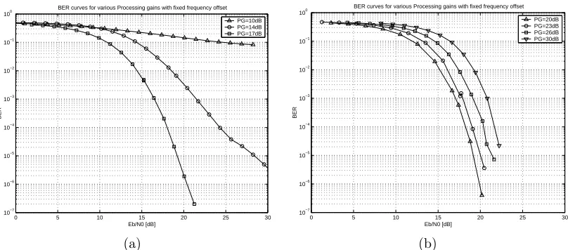
100 BER curves for various Processing gains with fixed frequency offset
Eb/N0 [dB] BER PG=10dB PG=14dB PG=17dB (a)
0 5 10 15 20 25 30
10−7 10−6 10−5 10−4 10−3 10−2 10−1
100 BER curves for various Processing gains with fixed frequency offset
Eb/N0 [dB] BER PG=20dB PG=23dB PG=26dB PG=30dB (b)
Figure 3.4: BER curves for various processing gains, model 1
Later, when the system has been realized, these spectra will also be mea-sured.
3.4.2
BER curves
The main issue of the system simulation is determination of the BER curves for various processing gains. In Shang’s theoretical performance analysis, for each value for the processing gain, an error floor was found. Also, for each value ofEb/N0 an optimal value for the processing gain was determined.
First model
In Figure 3.4 the simulation results of the first model are presented. It can be seen that for low processing gains an error floor occurs. The error floors for the higher processing gains are present, but could not be calculated as a consequence of the extremely long simulation times.
When comparing these simulation results with the theoretical results as found by Shang (Figure 2.6) , it can be seen that the basic behavior is equal, but there is not an exact fit. The high-processing gain simulations match reasonably well. For low processing gain values the theoretical performance is better than the simulated. For higher values it is the other way around.
3.4. RESULTS 23
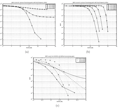
0 5 10 15 20 25 30
10−7 10−6 10−5 10−4 10−3 10−2 10−1
100 BER curves for various Processing gains with fixed frequency offset
Eb/N0 [dB] BER PG=10dB PG=14dB PG=17dB (a)
0 5 10 15 20 25 30
10−7 10−6 10−5 10−4 10−3 10−2 10−1
100 BER curves for various Processing gains with fixed frequency offset
Eb/N0 [dB] BER PG=20dB PG=23dB PG=26dB PG=30dB (b)
10 12.5 15 17.5 20 22.5 25
10−7 10−6 10−5 10−4 10−3 10−2 10−1 100
BER curves for df=3MHz with different processing gains
Eb/N0 (dB) BER PG=17 dB PG=20 dB PG=23 dB (c)
Figure 3.5: BER curves for various processing gains, model 3
Second model
The second model has only been used for generating the frequency spectra as shown in Figure 3.3. An offset frequency of 3 MHz has been applied. BER simulations could not be done because of the long simulation times involved.
Third model
The spreading sequence of the third model is a clipped version of the noise generated by the noise block, in order to have the same characteristics as the noise which will be used in the testbed. In Figure 3.5 the results of this simulations are shown.
Chapter 4
RF system design
The main goal of this master thesis project is the realization of a FODMA testbed. In the preceding chapters the FODMA system has only been de-scribed from a theoretical point of view. In practice however, components are used which do not show ideal behavior. For example, a coax cable of one meter introduces a phase shift of around 12λ and an attenuation of almost 1.5 dB for signals around 2.4 GHz.
In this chapter some basic RF design fundamentals are explained. Fur-thermore the characteristics and operation of RF mixers is explained.
4.1
Noise analysis
Noise is the enemy of most electrical engineers. It degrades system perfor-mance and, therefore, is a big issue. FODMA uses this ‘enemy’ as a bearer of the signal. Like in any other system, also unwanted noise is present. Ther-mal agitation of electrons is a main source of noise. The noise power as a consequence of this phenomenon is given by:
PT N =kT BN (4.1)
where k is Bolzmann’s constant, T is temperature in kelvin and BN is the
system’s bandwidth. The noise contribution of a component is typically given by its noise factor:
F = Sni
Sno
(4.2)
or the noise figure:
N F = 10 logSni
Sno
[dB] (4.3)
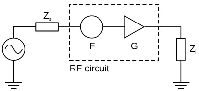
Zs
Zl
F G
RF circuit
Figure 4.1: Equivalent circuit for an RF component
where Sni stands for available SNR at the input and Sno for available SNR
at the device output.
In Haykin [6], the Noise Figure is defined as: “the ratio of the total avail-able output noise power (due to the device and the source) per unit bandwidth
to the portion thereof due solely to the source”.
For low-noise devices, the values of the noise factor are close to unity, which makes comparison with other low-noise devices difficult. For these cases the noise characteristics can be described in an alternative way, using
the equivalent noise temperature. First, the RF circuit is decomposed into
two elements: an ideal amplifier with gainGand a noise source (F) as shown in Figure 4.1.
When the in- and output impedances are matched to the source- and load impedance, the available noise power at the input of this equivalent circuit is:
Ns =kT BN (4.4)
The noise power contributed by the device itself can be given by:
Nd=GkTeBN (4.5)
The variable which is introduced here,Te, is called the equivalent noise
tem-perature. With this new definition of Nd, the output noise power can be
given by:
N0 = GNs+Nd
= Gk(T +Te)BN (4.6)
from which we can derive
F = N0
GNs
= T +Te
T
4.2. FREQUENCY SHIFTING OPERATIONS 27
When cascading components, the noise factor of the entire system can be determined as follows:
No = G1G2Ns+G2Nd1+Nd2
= G1G2k
µ
T +T1+
T2
G1
BN (4.8)
When comparing equation 4.8 with equation 4.6 we can see that the equiva-lent noise temperature of the cascaded system is given by:
Te=T1+
T2
G1
(4.9)
This can be expanded for an arbitrary number of networks to:
Te =T1 +
T2
G1
+ T3
G1G2
+. . .+ QnT−n1
i=1 Gi
(4.10)
or, rewritten to the noise figure F as:
FN =F1+
F2 −1
G1
+F3−1
G1G2
+. . .+QFnn−−1 1
i=1 Gi
(4.11)
This equation is known as the Friis equation for cascaded noisy systems. From this equation it can be seen that the first components in a chain with positive gains have the biggest influence on the overall noise performance. It is for this reason that the front-end amplifier in a receiver should be a low-noise component.
4.2
Frequency shifting operations
A common operation in communication electronics is the shift of a signal from one frequency to another. This frequency shift can be implemented by multiplying the desired signal with the desired shifting frequency:
s(t) = m(t) cos(2πfct)·cos(2πfst)
= m(t)
2 [cos(2π(fc−fs)t) + cos(2π(fc +fs)t)]
The DC V-I characteristic of a diode can be expressed as:
I(V) = Is(eαV −1) (4.12)
α = q
nkT (4.13)
Let the diode voltage be:
V =V0+v (4.14)
where V0 is a DC bias voltage and v is a small AC signal voltage. When
expanding 4.12 in a Taylor series about V0 we get:
I(V) =I0+v
dI dV ¯ ¯ ¯ ¯ ¯V 0 + 1 2v
2 d2I
dV2
¯ ¯ ¯ ¯ ¯V 0
+. . . (4.15)
The constantI0 is a consequence of the applied DC bias. The first and second
derivative are found to be: dI dV ¯ ¯ ¯ ¯ ¯V 0
= αIseαV0 =α(I0+Is) = Gd =
1
Rj
(4.16)
d2I
dV2
¯ ¯ ¯ ¯ ¯V 0
= dGd dV ¯ ¯ ¯ ¯ ¯V 0
=α2(I
0+Is) =αGd=G
0
d (4.17)
now, equation 4.15 can be rewritten as:
I(V) = I0+i=I0+vGd+
v2
2G
0
d+. . . (4.18)
which is known as the small-signal approximation for diode behavior. In mixers, the v2 term is used to produce sum and difference frequencies
of a low-level RF signal and an RF local oscillator (LO) signal.
fIF =fRF ±fLO (4.19)
The simplest type of mixer is thesingle-ended mixer. RF and LO signals are typically given by:
vRF(t) = vrcosωrt (4.20)
vLO(t) = v0cosω0t (4.21)
When these two signals are combined and fed into a diode, the v2 term will
perform the desired frequency mixing operation:
i = G
0
d
2 (vrcosωrt+v0cosω0t)
2 = G 0 d 2 ³ v2
rcos2ωrt+ 2vrv0cosωrtcosω0t+v20cos 2ω 0t ´ = G 0 d
4 [v
2
r +v
2 0 +v
2
rcos 2ωrt+v02cos 2ω0t
4.3. DISTORTION 29
9 8 7 6 5
10
0 2 4 6 8 10
Local oscillator level [dBm]
Conversionloss[dB]
Figure 4.2: Typical conversion loss vs LO drive for 7dBm mixer
The terms of interest are those of frequencyωr±ω0, DC, 2ω0 and 2ωr terms
can be filtered out. Also the terms in the output that are generated by the
v term can be filtered out. From the equations above, it can easily be seen that not all input power is converted to the desired output signals. The ratio between these powers is called the conversion loss, and is given by:
Lc = 10 log
available RF input power
IF output power dB (4.23)
The conversion loss is dependent on the LO input power. The function of this LO drive is to switch the diode(s) in the mixer fully on and off, for the lowest possible distortion. The required LO drive power is a design parameter, mixers are available in a wide range of required LO powers. Most common are level 7 mixers, which require 7 dBm LO input power.
When a mixer is driven at its required power, conversion loss is minimal. Small changes in driving power, around the designed power level, are not critical. A typical conversion loss vs. LO drive plot is given in Figure 4.2.
4.3
Distortion
When the Taylor expansion of diode behavior (Eq: 4.15) is generalized, we can write the transfer characteristics of any device as:
y(t) =α1x(t) +α2x2(t) +α3x3(t) +· · · (4.24)
When the input consists of a single sinusoidal wave x(t) = Acos(2πf t), the output of this system will be (ignoring fourth and higher order terms):
y(t) = 1 2α2A
2+ (α 1A+
3 4α3A
3) cos(2πf t)
+1 2α2A
2cos(4πf t) + 1
4α3A
This equation can be decomposed into fundamental, second harmonic and third harmonic frequency terms. Their amplitudes are:
Fundamental: α1A+34α3A3
Second harmonic: 1 2α2A
2
Third harmonic: 1 4α3A
3
With these amplitudes the second- and third-order harmonic distortion is found to be:
D2 = 1 2α2A
α1+34α3A2
(4.26)
D3 = 1 4α3A
2
α1+34α3A2
(4.27)
When the input is changed from one single sine wave to two waves with different frequencies, the third-order term α3x3(t) gives rise to
intermodu-lation products at the frequencies 2f1 ±f2 and 2f2 ±f1. These frequency
components have the following amplitudes:
2f1±f2: 34α3A21A2
2f2±f1: 34α3A1A22
From the foregoing section we may conclude that distortion is inevitable when using diode mixers. However, by using multiple diodes in a star- or ring configuration spurious products can be suppressed. For the FODMA testbed, double balanced diode mixers are used.
4.4
Power splitter
A power splitter is a three-port network with the task to split the power at the input and divide it over the two outputs. If all ports are matched, the scattering matrix of a three-port network is given by:
[S] =
0 S12 S13
S12 0 S23
S13 S23 0
4.4. POWER SPLITTER 31
Z0
Z0
Z0
2Z0
√ 2Z0
√ 2Z 0 λ/ 4 λ/4
Figure 4.3: Transmission line circuit of a Wilkinson power divider
|S12|2+|S13|2 = 1 (4.29a)
|S12|2+|S23|2 = 1 (4.29b)
|S13|2+|S23|2 = 1 (4.29c)
S∗
13S23= 0 (4.29d)
S∗
23S12= 0 (4.29e)
S∗
12S13= 0 (4.29f)
From equations 4.29d. . . 4.29f it follows that at least two of the three parameters (S12, S13, S23) must be zero, which is in contradiction with
4.29a. . . 4.29c. It follows that a three-port network cannot be lossless, re-ciprocal and matched at all ports at the same time.
Wilkinson developed a three-port power divider (Figure 4.3) which is lossless in power dividing, while being matched at all ports. It’s S-matrix is given by:
[S] =−√j
2
0 1 1 1 0 0 1 0 0
(4.30)
It can be seen from this matrix that this divider has ideal isolation from port two to port three and vice-versa. The power offered at port one is equally divided over the two output ports, without losses. However, this device is not lossless; when power is applied to port two or three, only half of the power appears at port one. The other half of the power is dissipated in the internal resistance between port two and three.
Chapter 5
Realization
5.1
Setup
Combining the knowledge from the simulations and the RF circuit design theory, components have been collected to realize the testbed. These com-ponents had to be compatible with the instruments already available in the lab and had to comply with high standards. First, a schematic drawing has been made of the entire system. In the drawing, rough values of the power levels in the entire system are given. These values have been derived from the required input powerlevels of each component. This drawing is given in Figure 5.1. In the following subsections the motivation for the use of each component is given.
5.1.1
Vector signal generator
The input signals to the system are generated by various signal generators. The signal used as a spreading sequence in the transmitter is generated by an Agilent vector signal generator which is capable of generating up to 50 MHz wide pseudo-random data sequence at any center frequency up to 6 GHz. A wide range of signal formats is available. In the FODMA system a BPSK constellation diagram is chosen. The center frequency is 2.4 GHz. The data is generated by a PN23 pseudo random noise generator.
5.1.2
Mixers
The entire transmitter and receiver chain of the FODMA system contains four frequency mixers, which have to perform three unique tasks. In the transmitter, the data which are to be transmitted have to be modulated on
N(t) Noise Sine Data LO LO LO LO RF RF RF RF 7dBm 0dBm 7dBm 7dBm 7dBm 0dBm 10dBm 3dBm fc=2.4GHz
BW = 50MHz BW = 500KHz
fc=5MHz -10dBm -10dBm 10dBm -10dBm -10dBm +10 IF IF 0dBm IF IF LPF +25dB -5dB clk Out +10 -3dB
Figure 5.1: Schematic drawing of the FODMA system
the broadband noise carrier. Also, the reference noise has to be shifted in frequency.
At the receiver side, one mixer performs the same frequency shifting op-eration as in the transmitter. The task of the fourth mixer is to despread the transmitted data back to the baseband. For the best performance, a linear operation in the desired frequency range is desired. Also low distortion and low third-order intermodulation products are required.
The operating frequency of the mixers in the RF band is around 2.4 GHz. For the characteristics around this center frequency to be maximally flat, mixers with a much wider bandwidth are chosen. The IF port should work from DC to at least the largest required offset frequency (df ÀBdata).
Finally, a mixer from Minicircuits has been chosen (ZX05-30W, [7]), which has an LO/RF frequency range from 300 to 4000 MHz and an IF range from DC to 950 MHz. The required LO drive power is +7 dBm.
5.1.3
Splitters
The main issue in splitters is, as in other components, low losses. From theory we know that Wilkinson power dividers show ideal splitting behavior. The only disadvantage of a single Wilkinson structure is the small bandwidth. Minicircuits has developed a ultra wide band power splitter (ZN2PD2-50, [8]), which consists of a series of seven Wilkinson dividers. The bandwidth of this splitter ranges from 500 to 5000 MHz. Due to losses in the materials and connectors, the insertion loss of this splitter is not only the -3dB because of the split, but there is an additional loss of 0.8-1.4dB.
5.1. SETUP 35
which is designed for a small band around 2.4 GHz? The easy answer is that there were already two splitters of this type available. The more satisfying answer is that it is more profitable for the microwave communication lab to invest in a device which is suitable for a wider frequency range, so that it can be used for other applications as well.
5.1.4
Amplifiers
From the Friis equation for cascaded systems (4.11) it follows that the first component in a cascaded system with positive gains dominates the overall noise performance of a system. For this reason it is important to pick a very low-noise high gain amplifier as front-end amplifier. It can be deduced from Figure 5.1 that the power level at the output of the amplifier should be around +10 dBm. The input power level will be somewhere around -10 dBm, so at least 20 dB amplification is needed.
With the noise figure and bandwidth requirements, eventually the Mini-circuits ZRL-2400LN [9] amplifier has been selected. This amplifier has a 25 dB gain, with a noise figure of 1.2 dB typical. The frequency range of this amplifier ranges from 1000 to 2400 MHz, which is sufficient for our system.
From Figure 5.1 it can also be seen that in the receiver, a second am-plifier is needed. This amam-plifier compensates for the conversion loss in the frequency-shifting mixer. Operation is possible without this amplifier but then the total output power would be lower than -20 dBm while when using this amplifier, the output level will be higher.
The desired RF input level of the last mixer in the system is 0 dBm, thus a 10 dB amplifier is needed. From the IC Design (ICD) group, a Minicircuits 10 dB amplifier of the type ZJL-7G [10] could be borrowed. This amplifier has a frequency range from 20 to 7000 MHz with a noise figure of 5 dB.
After filtering of the output, another +10 dB amplification is applied, which gives us an output signal between 10 and 100 mV. Since the signal of interest is a baseband signal, this amplifier needs to amplify from DC to at least the signal’s bandwidth. The ICD group also supplied an EG&G parc wide-band preamplifier from DC to 70 MHz, with a selectable gain of 10 or 20 dB.
5.1.5
Filters
filter (SLP-2.5, [11]) which filters out frequencies above 2.5 MHz. From 3.8 to 5 MHz, the losses are more than 20 dB, above 5 MHz more than 40 dB.
The second filter is an active Krohn-Hite filter (model 3202). It has a variable cutoff frequency between 20 Hz and 2 MHz with slopes of 24 dB/octave. Despite of noise considerations, this filter is placed before the last amplifier. This is to prevent overloading the final amplifier.
5.1.6
Other components
For optimal demodulation, it is important that the information bearing noise arrives in phase with the reference noise at the correlator. This can be obtained by inserting a coaxial phase shifter in one of the branches of the receiver.
When determining BER curves as a function of signal power over noise power, it must be possible to control the signal- or the noise power. The added noise should not be correlated to the transmitted signal. Since there are not two signal generators capable of generating a 50 MHz noise signal available in the microwave lab, another solution for generating the ‘channel noise’ had to be found. The method applied in my measurements uses the fact that the correlation time of a (pseudo-)random noise source is very short. The noise generated by the vector signal generator is split. One branch is used as a spreading sequence in the transmitter, the other branch is delayed by sending it over 40 meters of coax cable to obtain a delay of approximately 200 ns. This delay equals ten bit-times of the noise source, which is enough for the noise to be uncorrelated with its time-shifted version. To compensate for the signal attenuation in the cables, two amplifiers of the type MAX2242/3 are used. These amplifiers provide a 28.5 dB gain and compensate for the 1.5 dB/m cable loss. The power level of the noise can be controlled by two cascaded variable attenuators, the HP 8494B/11dB and the HP 8495B/70dB. With these attenuators, the channel noise power can be attenuated in steps of 1 dB from 0 to 81 dB.
All cabling is standard RG316 50-ohms cable with SMA connectors.
5.1.7
Equipment
5.2. MEASUREMENTS 37
LO RF LO RF
IF
LO RF IF
LO RF
IF
IF +25dB
-3dB FuncGen1
VSG
FuncGen2
DataGen
ErrDet
+28dB
+10dB
Fc=2.5M Fc=Bd
+28dB
+10dB
Figure 5.2: Schematic drawing of the FODMA testbed
Function Component
Vector signal generator Agilent E4438C ESG Data generator HP 3762A
Error detector HP 3463A
Function generator 1 Rhode&Schwartz SMS
Function generator 2 HP 33120 Function Generator Spectrum analyzer HP 8593E
Oscilloscope HP 54600A Phase shifter Nardia 3752
With these components the setup as given in Figure 5.2 has been built.
5.2
Measurements
Before presenting the first measurement results a short introduction of the performed measurements and measurement techniques is given.
For determining BER curves as a function of the available signal to noise ratio, some important definitions have to be stated first.
Output signal power: The power measured directly at the output of the transmitter in a 50 MHz band around 2.4 GHz.
C/N: The ratio between the Output signal power and the channel noise power.
SNR: C/N plus the processing gain.
5.2.1
Power levels
For power measurements, a spectrum analyzer has been used. In order to make an accurate measurement, the signal of interest is averaged over 100 samples before showing on the display. Since the dynamic range of the sig-nals is very large, the spectrum analyzer is set to a log (dB) display mode. However, we must be careful with the measurement results obtained this way for the following reason: the log of the average is not equal to the average of the log! Due to the log scaling, noisy peaks are compressed while dips are ex-panded towards minus infinity dB! This causes the measured average power in a frequency band to be lower than the actual value. For noisy signals, a fixed correction factor of +2.51dB has to be applied [12].
At frequencies around 2.4 GHz, cable losses are of major influence. Cable loss per meter, is 1.5dB.
The correction factor and losses mentioned above are only of interest when we are interested in absolute power levels at in- or output ports of the components used. For the SNR measurements they are of no interest, as long as the measurements are performed with the same set of cables.
5.2.2
BER measurements
For making BER measurements, we need a device which is capable of gener-ating a NRZ (pseudo-)random data sequence that can serve as data input for the transmitter, and a receiver which is capable of comparing the output data of the receiver with an internally generated and synchronized version of the same sequence. For this goal, the HP 3762A data generator and HP 3463A error detector are used. These devices are capable of handling datarates be-tween 1 Kbps and 150 Mbps. For statistically reliable results, the BER is calculated after counting a fixed number of errors which is in our case 100 errors.
5.3
Results
5.3. RESULTS 39
5.3.1
Frequency spectra
Power spectra at all important points in the system are measured to check whether they match with our predictions. In Figure 5.3 the spectrum at the transmitter side is shown. As can be seen in Figure 5.3(b), the spreading sequence is not exactly 50MHz wide but a little broader, with small sidelobes. Raised cosine filtering with a factor alpha = 0.1 is applied to reduce the amount of power in the sidelobes. Furthermore it is important to note that the 2.4GHz carrier is present in the spreading sequence. In Figure 5.3(d) the shifted versions of the carrier frequency can be seen at fc ±3M Hz. These
carrier frequencies are of major importance to the performance of the system, as will be shown next.
In Figure 5.4 the spectrum at the receiver’s side is shown. In Figure 5.4(a) the frequency offset is applied again. It is clear that the carrier frequency is present again at 2.4GHz. Not so easily seen are the peaks at 2400 ±3 and
±6 MHz. These peaks mix back in the last mixer to the integer multiple frequencies of 3 MHz in Figure 5.4(b). Not shown in this figure are the higher frequency components that are predicted by Equation 2.10, however, they are present around 2.4 and 4.8 GHz. The first filter removes these high frequencies. After this first filter, the second filter, which is matched to the data bandwidth removes the other higher frequency components. As can be seen in Figure 5.4(f) the 3MHz component is effectively suppressed by this filtering, which makes detection of the original signal possible using the error detector.
The measured spectra match our predictions, based on the simulation results (Figure 3.3). The mixers behave according to specifications. With the applied filtering and amplification an output signal has been realized which can serve as input for the error detector.
5.3.2
BER measurements
After determining the spectra in the system, the real work could begin: de-termination of the BER curves. The BER curves have been measured for different values of the processing gain and for a number of frequency offsets.
BER versus processing gain
Figure 5.5 shows the result of the first measurements. It can be seen that there is something strange going on from Eb/N0 = 26 . . . 27. On the
(a) Data input (b) Spreading sequence
(c) Spreading sequence x Data (d) Spreading sequence x Frequency
offset
(e) Transmitter output
5.3. RESULTS 41
(a) Received signal x Frequency offset (b) Output signal, DC-10MHz
(c) Output signal, DC-1.5MHz (d) Output signal, DC-10MHz, filter 1
(e) Output signal, DC-1.5MHz, filter1 (f) Output signal, DC-10MHz, filter 2
(g) Output signal, DC-1.5Mhz, filter2
24 26 28 30 32 34 36 10−6
10−5 10−4 10−3 10−2
10−1 BER curve for 20 dB Processing Gain with 15 MHz frequency offset
Eb/N0 (dB)
BER
Figure 5.5: BER curve from FODMA with a 15 MHz frequency offset
0 1 2 3 4 5 6 7 8 9 10
−100 −90 −80 −70 −60 −50 −40 −30 −20
Phase shift in HP 8494B 11dB variable attenuator
Attenuation (dB)
Phase shift (degrees)
Fc=2.375 GHz Fc=2.4 GHz Fc=2.425 GHz
Figure 5.6: Phase shifts in the HP 8494B variable attenuator
attenuation of the attenuators has been measured using a spectrum analyzer and showed no irregular behavior. However, the phase shift in the attenu-ators turned out to be attenuation dependent, as can be seen from Figure 5.6. Since the noise is not real gaussian noise but a pseudo-random BPSK sequence around 2.4 GHz, this phase shift is crucial for the system perfor-mance. The output signal is, as said before a pseudo random BPSK sequence around 2.4 GHz. The constellation diagram of BPSK modulation lies entirely on the real axis of the I/Q plane. When the noise, which also is a BPSK sequence, is added to the output signal and this noise is orthogonal to the output signal, it is of no influence to the system.
5.3. RESULTS 43
ICD/S&S group, a 50 MHz wide noise source with 4-QAM modulation has been generated. By using the QAM modulation, this channel noise occupies the entire I/Q plane and thus will not be purely orthogonal to the output signal. Also, by using this second VSG, it was not necessary to use the variable attenuators anymore, since the output power could be controlled at the VSG itself.
With this new setup, the results as shown in Figure 5.7 have been ob-tained. In Figure 5.7(a) the BER curves for low processing gain factors are shown. Here, the predicted error floors are clearly observed. In Figure 5.7(b) and 5.7(c) no error floors are visible. The error floors for these processing gains are so low that measurement is no longer practical.
In Figure 5.7(d) the BER curves for processing gains of 17, 20 and 23 dB obtained by measurements are given together with the analytical results (dashed) for these processing gains. It can be seen that the performance of the testbed is about 10dB worse than predicted from theory. This difference can mainly be attributed to signal losses in the components.
BER versus frequency offset
The FODMA is designed to be a multiple user system. Each user can have their own channel in the same frequency band when an unique frequency off-set is assigned. This frequency offoff-set must be in the rangeBdata¿df ¿Bss.
Measurements have been done for offset frequencies between 3 and 15 MHz. While doing these measurements, the output power of the system turned out to be dependent on the applied offset frequency. Also, to obtain max-imum output power, the phase shift applied by the coaxial phaseshifter in the upper branch of the receiver (see Figure 5.2) had to be adjusted for each offset frequency. In Figure 5.8 the phase shift for maximum output power is plotted together with the output power in the frequency band from 0 . . . 1 MHz at this optimal phase shift.
Apparently, there is an IF-port frequency dependent phase shift in the mixers! Unfortunately, measurement of the phase shift in mixers as a function of IF input frequency could not be carried out.
As can be expected from Figure 5.8, the performance of the testbed is optimal at an offset frequency of 3 MHz, since the output power has a peak at that frequency. In Figure 5.9 the measurement results for frequency offsets between 3 and 15 MHz are given. In Figure 5.9(d) the BER is plotted versus the applied offset frequency at Eb/N0 = 36.6dB. It can be seen that the
20 25 30 35 40 45 10−7 10−6 10−5 10−4 10−3 10−2 10−1
100 BER curves for df=3MHz with different processing gains
Eb/N0 (dB) BER PG=15.3 dB PG=16 dB PG=17 dB PG=18.3 dB (a)
20 25 30 35 40 45
10−7 10−6 10−5 10−4 10−3 10−2 10−1
100 BER curves for df=3MHz with different processing gains
Eb/N0 (dB) BER PG=20 dB PG=21.3 dB PG=23 dB (b)
20 25 30 35 40 45
10−7 10−6 10−5 10−4 10−3 10−2 10−1
100 BER curves for df=3MHz with different processing gains
Eb/N0 (dB) BER PG=26 dB PG=29 dB PG=30 dB (c)
15 20 25 30 35 40
10−7 10−6 10−5 10−4 10−3 10−2 10−1 100
BER curves for df=3MHz with different processing gains
Eb/N0 (dB) BER PG=17dB PG=20dB PG=23dB (d)
Figure 5.7: Measurement results of BER versus Processing Gain
2 4 6 8 10 12 14 16
100 105 110 115 120 125 130 135
Phase shift [degrees]
2 4 6 8 10 12 14 16−29
−28 −27 −26 −25 −24 −23 −22
Received power [dBm]
Phase shift
Received power
5.3. RESULTS 45
20 25 30 35 40 45 50
10−7 10−6 10−5 10−4 10−3 10−2
10−1 BER curves for 20 dB Processing Gain with different frequency offsets
Eb/No (dB) BER df=3MHz df=4MHz df=5MHz df=6MHz df=7MHz (a)
20 25 30 35 40 45 50
10−7 10−6 10−5 10−4 10−3 10−2
10−1 BER curves for 20 dB Processing Gain with different frequency offsets
Eb/No (dB) BER df=8MHz df=9MHz df=10MHz df=11MHz (b)
20 25 30 35 40 45 50
10−7 10−6 10−5 10−4 10−3 10−2
10−1 BER curves for 20 dB Processing Gain with different frequency offsets
Eb/No (dB) BER df=12MHz df=13MHz df=14MHz df=15MHz (c)
2 4 6 8 10 12 14 16
10−7 10−6 10−5 10−4 10−3
10−2 BER curve for 20 dB Processing Gain at Eb/Np = 33.6 dB
Frequency offset (MHz)
BER
(d)
34 35 36 37 38 39 40 41 42 43 44 10−6
10−5 10−4 10−3 10−2
10−1 BER curves with small band jamming signals
Eb/N0 (dB)
BER
Fc=2.4GHz Fc=2.41GHz Fc=2.42GHz
Figure 5.10: BER curves for in-band jamming signals, PG=20dB
In-band jamming
Ultra-wideband systems use an extremely high bandwidth. By despreading the signal in the receiver, the original data sequence is retrieved. As a con-sequence of the spreading, UWB systems are robust to small-band jamming signals. Using the second VSG, a 1 MHz wide jamming signal (QAM, pseudo random noise) has been generated. This jamming signal was varied in power and in center frequency.
In Figure 5.10 the signal output power was -12 dBm. The noise power in the 1 MHz jamming signal was varied from -16.7 to -25.7 dBm, at center frequencies of 2.4, 2.41 and 2.42 GHz. The system performance under influ-ence of small band jammers turns out to be dependent on the position of the jamming signal. It is clear that the farther the jamming signal is from the center frequency of the spreading sequence, the better the performance.
Theoretically speaking the position of a jamming signal should not influ-ence the system’s performance. The explanation is probably associated with the generation of the spreading sequence. As mentioned before, the noise signal contains the signal’s carrier frequency. This frequency is shifted in the transmitter and receiver, in the end it is present atfc, fc±df andfc±2df.
The small band jamming signal will mix back efficiently to the baseband due to these frequency terms.
5.4
Wireless operation
5.4. WIRELESS OPERATION 47
Noise Noise
Data
fc=2.4GHz BW = 50MHz
fc=3MHz
+25dB
Tx +25dB +28dB Rx
Sine
BW=1MHz
2Mtr 2Mtr
Figure 5.11: FODMA setup for wireless transmission
20 21 22 23 24 25 26 27
10−6 10−5 10−4 10−3 10−2
10−1 BER curves for various processing gains, wireless transmission
Processing Gain (dB)
BER
Noise = none Noise = 0dBm Noise = 5dBm
Figure 5.12: Measurement results for wireless transmission with varying pro-cessing gains
The setup as shown in Figure 5.11 was used to determine the performance in a multipath environment.
Note that since these measurements were done in an office environment, the multipath effects could not be controlled. Shifting a chair in the vicinity of the transmitter or receiver caused the received signal to change dramatically.
BER versus processing gain
2.375 2.38 2.385 2.39 2.395 2.4 2.405 2.41 2.415 2.42 2.425 10−5
10−4
10−3
10−2
10−1 BER curves with small band jamming signals
Center frequency of jamming signal
BER
PG=26 dB PG=23 dB PG=20 dB
Figure 5.13: Measurement results for wireless transmission with in-band jam-ming
In-band jamming
In the wireless testbed, a small band jamming signal was also generated. The signal had a fixed power and was varied in frequency from 2.375 to 2.425 GHz.
Chapter 6
Conclusions and
recommendations
In this report the results of the work done for simulation and realization of an FODMA testbed have been presented. The system has been simulated in ADS, using three different simulation models. The testbed has been realized with standard off-the-shelf microwave components.
6.1
Conclusions
Simulation results
The simulation parameters were set according to the system specifications of the testbed to be realized. The bandwidth of the spreading sequence was 50 MHz. By choosing bit rates from 50 Kbps to 5 Mbps the processing gain was varied from 10 to 30 dB. The simulation results (Figure 3.4 and 3.5) do not exactly match with the predictions from theory (Figure 2.6). The most important reason for this