Available online: https://edupediapublications.org/journals/index.php/IJR/ P a g e | 933
A Novel Method for 64-Bit BCD Add-Subtract Unit Design by
Reversible Using Parallel Pipelined Method
M.Sumanth Chaitanya & S.Raghavendra
1 Lecture,Department of ECE, JNTUA College of Engineering ,Dist Anantapuram , AndraPradesh, India 2 Asst.Professor, Department of ECE, Dist Anantapuram , AndraPradesh, India.
Abstract
Arithmetic unit design using reversible logic gate has received much attention as it reduces power dissipation with no loss of information. This paper proposes the design of 64-bit Binary Coded Decimal (BCD) addition and subtraction unit using reversible logic gates. The reversible 64 -bit BCD addition unit is designed using the following modules such as reversible 4-bit Carry Propagate unit using reversible logic gates such as Feynman gate and URG gate and a reversible 4-bit error correction unit. The 4-bit error correcting unit designed by reversible (4x1) Multiplexer (MUX) unit using Toffoli gate and TNOR gates to provide the output with a precise value. The reversible 64-bit BCD subtraction unit is designed based on the nine’s complement method of 4-bit reversible BCD addition. In BCD subtraction unit, the error correcting block is designed with the conditional reversible logic COG gate to make the necessary corrections at the output to get exact output. The reversible 64- bit BCD addition and subtraction unit is designed based on the parallel pipelined unit to enhance the speed of operation. This proposed reversible 64-bit BCD addition module has 416 garbage values with the critical path delay of 17.420 ns; reversible 32-bit BCD subtraction module has 240 garbage values with the critical path delay of about 17.420 ns.
Index Terms— Reversible logic gates; BCD adder; BCD subtractor, Reversible add-subtract unit.
I. INTRODUCTION
Reversible logic is the effective alternative in the design of
low power arithmetic unit. The reversible logic gate, which has one to one mapping technology provide output with zero loss of information. According to Bennett no energy would dissipate from a system if it would be able to return to its initial state from its final state regardless of what occurred in between [1]. In reversible logic gates input vectors can be retrieved from the output vectors with accuracy and low power dissipation. BCD employed on various digital processors decreases the delay of manipulation. BCD circuit may open new application areas of finance, commerce, land management and internet-based systems. BCD digit eliminates the truncation error and thereby reduces the computation delay. In this paper, BCD addition and subtraction unit has been implemented using the reversible logic gates. The addition and subtraction unit is designed for 32-bit input data using reversible logic gates. BCD adder and subtraction requires error correction unit which provides exact BCD output. The reversible logic gates such as Toffoli gate, Feynman gate, TNORG gate and URG gate are used in the design of reversible 64-bit BCD addition unit; SBV gate, TNORG gate, URG gate, Feynman gate, Toffoli gate and COG gate are used in the design of 32-bit reversible BCD subtraction unit. This proposed method will effectively reduce the delay, error and garbage values.
A. Reversible logic
Available online: https://edupediapublications.org/journals/index.php/IJR/ P a g e | 934
range such as low power optical computing, nanotechnology and quantum computing. One to one mapping of input and output vectors of reversible logic gates prevents the gate from loss of information in the form of heat energy. Reversible logic gates reduce the loss of information when repossessing the input vectors from output vector. Input vectors of the reversible logic gates are 0‟s and 1‟s; the output vectors comprise of output values and the garbage values. These garbage values along with output values helps in retrieving the input vectors without any loss in information. Reversible logic gates are more effective in implementing the Boolean expressions with high accuracy. Reversible logic gates do not allow fan-out whereas cascading of reversible logic gates is possible [3]. This paper proposes the design of BCD adder and subtraction for 32-bit input data using reversible logic gates.
II. LITERATURE SURVEY
In the existing design, X. Susan Christina, M.Sangeetha Justine, K.Rekha, U.Subha and R.Sumathi designed BCD addition and subtraction unit is designed using the reversible logic gates. A 4-Bit Reversible BCD addition unit is designed as ripple carry adder, carry skip adder, carry select adder and carry look-ahead adder using reversible logic gate named NEW gate, Feynman gate, TSG gate, Toffoli gate, Fredkin gate. The comparative result of reversible 4-bit BCD adder is provided with the delay of manipulation. From the existing module of comparison carry look-ahead adder has the lowest delay of manipulation of about 456.774ns with the garbage values of 48 [4]. V. Rajmohan, V. Renganathan, and M. Rajmohan proposed a 4-bit BCD Subtraction unit is realized by obtaining nine‟s complement of one of the 4-bit input vectors and is added using the 4-4-bit BCD adder unit. The reversible logic gates such as TKS gate, SCL gate, HNG gate, Peres gate, BVF gate have been used in
the design of 4-bit reversible BCD subtraction unit. The delay of manipulation of reversible 4-bit subtraction unit is estimated in the existing work is about 36ns with the garbage value of 37 [5]. Robert D. Kenney and Michael J. Schulte proposed the design of BCD using double error correction unit for addition. The addition is performed using the Carry Save adder and Carry Propagate Adder in the form of a tree structure with double error correction unit to reduce the error of manipulation [6].
III. PROPOSED DESIGN
In this paper, reversible logic gates are used to realize the 32-bit BCD addition and subtraction units. Reversible logic gates are employed so as to reduce the delay and power dissipation in the BCD arithmetic unit. BCD adder adds two input data and produces the sum as the result. On account of any error in the sum value like the output data so generated is not a BCD number then there needs a correction block for the error output so produced [7]. Reversible BCD subtraction unit subtracts the two input values and generates the difference value as the output. In the proposed design, subtraction is realized by taking the nine‟s complement and adding the complemented value along with the other input data [8].
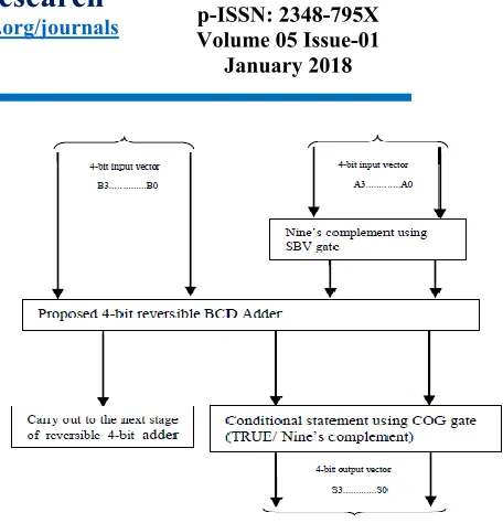
A. Reversible 32-bit BCD Addition
Available online: https://edupediapublications.org/journals/index.php/IJR/ P a g e | 935 Fig. 1. Proposed 4-bit reversible BCD Addition unit
The generated output from 4-bit adder unit is checked for error using error correction unit. Error correction block is designed by (4x1) MUX using Toffoli gate and TNORG gate. If the output of (4x1) MUX is „1‟ then the value of binary „0110‟ is added with the output of stage 1 of reversible 4-bit BCD adder; else the output is generated without any correction.
By cascading 8 reversible 4-bit BCD adder along with the error correction block, 64-bit reversible BCD addition can be realized as shown in Fig. 2.
Fig. 2. Proposed reversible 64-bit BCD adder
B. Reversible 32-bit BCD Subtractor
Reversible 32-bit BCD subtraction unit is designed based on addition of nine‟s complement of one of the two 4-bit inputs and is added with the other 4-bit input value.
Fig. 3, the error correction block is designed for individual 4-bit BCD addition blocks
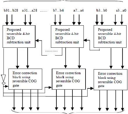
Available online: https://edupediapublications.org/journals/index.php/IJR/ P a g e | 936 Fig. 4. Proposed 64-bit reversible BCD Subtract unit
From Fig. 4, it is inferred that the 64-bit BCD subtraction is realized by cascading of eight 4-bit reversible BCD subtraction units along with the error correction block manipulated for individual reversible 4-bit BCD subtraction.
IV. RESULT AND DISCUSSION
Fig.5, shows the simulation result of reversible 32-bit BCD addition unit which have been designed. The vectors sum1, sum2, sum3, sum4, sum5, sum6 and sum7 are the 4-bit BCD adder output that acts as an intermediate blocks to generate the output vectors. Reversible 32-bit BCD adder so designed, calls the reversible 4-bit BCD addition 8 times to generate the output of 32-bit reversible BCD adder Addition is performed based on the CPA fashion using reversible logic gates for individual 4-bit BCD input vectors. The error correction is made depending on the output of the (4x1) MUX designed using reversible logic gates.
Fig. 5. Simulation result of reversible 32-bit BCD Addition unit
From Fig. 5, simulation result, vectors a and b are the input; sum provides the output values of the 64-bit BCD addition.
Fig. 6. Simulation result of reversible 64-bit BCD Subtraction unit
Fig. 6, shows the simulation result of reversible 32-bit subtraction unit. The subtraction unit is designed using the nine‟s complement of one of the 4-bit input data and is added using the proposed reversible 4-bit BCD addition unit.
Available online: https://edupediapublications.org/journals/index.php/IJR/ P a g e | 937
correction block of proposed 64-bit reversible BCD subtraction unit.
TABLE-I SYNTHESIS REPORT FOR REVERSIBLE 32 BIT BCD ADD UNIT
TABLE-II SYNTHESIS REPORT FOR REVERSIBLE 32 BIT BCD SUBTRACT UNIT
Reversible 32-bit BCD subtraction module has about 240 garbage values with the critical path delay of about 17.420 ns.
TABLE-III COMPARISON TABLE OF PROPOSED REVERSIBLE BCD ADDITION AND SUBTRACTION UNIT WITH THE EXISTING UNIT
From table III, the proposed design of 32-bit addition and subtraction unit are efficient with reduced delay of manipulation when compared to the existing modules designed for 4-bit input vectors.
V. CONCLUSION
In this paper, the design of 64-bit BCD add- subtract unit have been implemented using reversible logic gates. Modules such as 4-bit BCD addition, error correction unit, (4x1) MUX, conditional statements, 4-bit nine‟s complement unit have been designed using the reversible logic gates. BCD arithmetic units are speedy manipulation with reduced area. The four bit BCD addition is designed in the CPA fashion to further enhance the speed of 32-bit BCD arithmetic design for add- subtract units. 32-bit subtraction unit have been designed using 4-bit nine‟s complement and 4- bit BCD addition unit. The proposed module has wide range of application in digital signal processing. The estimated parameters for reversible 32-bit BCD addition unit is about 416 garbage values with the critical path delay of 17.420 ns; reversible 32-bit BCD subtraction module is about 240 garbage values with the critical path delay of about 17.420 ns.
REFERENCES
[1] C.H.Bennett, “Logical Reversibility of
Computation,”
IBM
J.Research
and
Development, pp.525-532, November 1973.
[2] R.Landauer, “Irreversibility and Heat
Generation in the Computational Process,” IBM
Journal of Research and Development, 5,pp.
183-191, 1961.
Available online: https://edupediapublications.org/journals/index.php/IJR/ P a g e | 938