Design of a Multi-Mode Interference Crossing Structure for Three
Periodic Dielectric Waveguides
Haibin Chen1, Zhongjiao He2, and Wei Wang1, *
Abstract—Based on the multi-mode interference effect in the periodic dielectric waveguide, a novel waveguide crossing structure is proposed and analyzed. The structure can achieve crossing connection of three periodic dielectric waveguides at the same position with low crosstalk and relative high transmission coefficient. Based on electromagnetic numerical simulation methods, the proposed crossing structure of three periodic dielectric waveguides is calculated and analyzed in details, and at the optical communication wavelengths near 1.55µm, crosstalks below 22 dB between the three crossing periodic dielectric waveguides are achieved.
1. INTRODUCTION
Since the first laser appearing in 1960, various kinds of optoelectronic devices, systems and commercial products have gradually come into human life. However, the conventional optoelectronic systems use separate devices, which results in huge volume, sensitivity to temperature, air disturbance, and mechanical vibrations. To solve the problems, in 1969, Miller of Bell Lab. proposed the concept of integrated optical circuits, and the basic idea is using optical dielectric waveguides as the basic connecting components and using lithography technology to fabricate lasers, modulators, filters, etc. to construct laser circuits to substitute the conventional optoelectronic systems [1]. Nowadays, photonic integrated circuits (PICs) or opto-electronic integrated circuits (OEICs) have been an independent and important development direction of optical and optoelectronic devices and systems.
Besides connecting of devices using optical dielectric waveguides, main devices of PICs or OEICs also commonly use optical dielectric waveguide structure, so optical dielectric waveguides are the fundamentals of PICs or OEICs. Properties and fabrication processes of optical dielectric wavegudies directly determine the overall performances of PICs or OEICs. However, conventional optical dielectric waveguides are all based on the mechanism of totally internal reflection [2], the confinement ability for the propagating light is relatively weak, so the waveguide cannot be bent too much. In addition, the connecting waveguides of optical devices in PICs or OEICs usually cannot cross each other, so the integrated size cannot be effectively reduced.
Recently, a type of one-dimensional periodic dielectric waveguides (PDWGs), for their relatively simple structure, versatile design, and low bending losses with sharp bending angles, have attracted much attention from researchers [3–14]. Through a theoretical study based on numerical simulation, Luan and Chang [12] showed that a kind of one-dimensional periodic dielectric rod waveguide could achieve high transmission even with acute angle bend. With a bend radius of 3λ(λis the wavelength), a transmissivity better than 90% was achieved, which is difficult for conventional waveguides [12]. In 2010, Li and his coworkers at Tsing Hua University experimentally studied the cross connection of two perpendicular PDWGs based on the SOI (Silicon on insulator) platform [13]. In their experiment, the
Received 29 January 2018, Accepted 30 March 2018, Scheduled 16 April 2018
* Corresponding author: Wei Wang ([email protected]).
between the two waveguides is less than −40 dB. Li and his group at Sun Yat-Sen University also proposed a PDWG crossing design based on a resonant cavity structure, which achieved a crosstalk lower than 0.8% [14]. The current researches on PDWGs show that the PDWG structure may be used to substitute conventional dielectric waveguides with the advantage of greatly decreasing PIC sizes.
In previous work, a cross structure can only achieve the direct cross connection of two waveguides. In this paper, a direct crossing structure for three waveguides based on the multi-mode interference (MMI) effect of PDWGs is proposed. Low crossing connection of three PDWGs crossing at a same position is realized, and transmission properties of the structure are calculated and analyzed in details based on finite-difference time-domain (FDTD) simulation and a plane wave expansion (PWE) method [15, 16].
2. DISPERSION PROPERTIES AND MULTI-MODE INTERFERENCE EFFECT
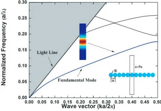
For the design of a PDWG cross connection structure, the basic construction units are single mode and multi-mode PDWGs. Therefore, dispersion and transmission properties of single mode and multi-mode PDWGs are studied firstly. The considered one-dimensional (1D) PDWG consists of circular dielectric pillars, as shown in the inset of Fig. 1. Lattice period of the PDWG isa. All the dielectric pillars have the same radius of R= 0.5a. Refractive index of the dielectric pillar is set as 3.4, and the background material is supposed as air with an index of 1. Through a PWE method, the dispersion properties of the PDWG are calculated. As shown in Fig. 1, the PDWG is single mode in a wide frequency range. In this paper, only TE mode is considered, of which the electric field vector is perpendicular to the propagation direction and parallel to axial direction of the dielectric pillars.
Figure 1. Dispersion curve of a 1D PDWG, in which, the waveguide structure, and field distribution of the fundamental mode are also given, it is mirror symmetric about propagation axis of the waveguide.
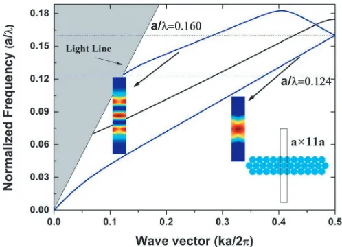
Figure 2. Dispersion curves of a multi-mode PDWG, in which, the waveguide structure, mode distributions of the 0th and 2nd modes are also given.
in the inlets of Fig. 2, and they are both with an even symmetry about the propagation axis of the multi-mode PDWG.
Considering mode interference effect of the 0th and 2nd modes, along the multi-mode PDWG, self-imaging phenomenon will appear, of which the period is
Li = β 2π
2−β0
According to this formula, for optical waves with normalized frequency ina/λ = 0.124∼160, the self-imaging period is in the range of 3.92a∼4.53a, as shown in Fig. 3.
For an optical wave with a normalized frequency of a/λ = 0.145, the self-imaging period is 4.2a. By the FDTD method with a perfectly matched layer (PML) boundary condition, a continuous optical wave with a normalized frequency ofa/λ= 0.145 is incident into the single mode PDWG, and the multi-mode PDWG is excited in the center position of its left side. The optical power density distribution can be obtained as shown in Fig. 4. It can be seen that self-images of the input profile appear with a
Figure 3. Relationship between the self-imaging period and the normalized frequency of the multi-mode PDWG.
(a)
(b)
and is relatively far away from the boundary of the multi-mode PDWG. Therefore, if two multi-mode PDWGs are cross connected with each at one of the self-imaging positions, optical wave propagating in each PDWG can keep its original direction and will not be affected significantly by the disturbance of the waveguide boundary. Thus, this effect can be used to design PDWG cross connection structure with low crosstalk.
3. 3-PDWG CROSSING STRUCTURE AND TRANSMISSION PROPERTIES
Considering the hexagonal lattice characteristic of the MMI structure, a waveguide crossing structure of three PDWGs is designed, as shown in Fig. 5(a). Three single mode PDWGs are cross connected at the same position through three multi-mode PDWGs. The three multi-mode PDWGs are all chosen with the same length of 10aafter optimization, and the angle between any two PDWGs has the same value of 60◦. Letting the lattice perioda= 225 nm and using the FDTD method with a PML boundary condition, to simulate light propagation in the designed structure, propagation properties of the light incident from any single mode PDWG can be obtained. In Fig. 5(b), the transient optical wave field is given for an incident monochromatic optical wave with a wavelength of 1.55µm. It can be seen that for the light incident from left side of the horizontal waveguide, field of the optical wave is mainly concentrated on
(a) (b)
(c) (d)
the original waveguide, and only very little is coupled into the two inclined crossing waveguides. About 85.5% of the optical power is directly crossing through the cross coupling structure and propagates along the original direction. 6.2% of the optical power is reflected. Only 0.3% of the light power is respectively coupled into the left top and left bottom ports of the inclined crossing waveguides. 0.9% of the optical power is respectively coupled into the right top and right bottom ports of the inclined crossing waveguides. There is an energy loss of 5.9%, which should result from the scattering effect of the MMI crossing structure and has been changed into radiation mode of the background, as seen from Fig. 5(c). Obviously, most of the optical power is transmitted through the crossing structure and propagates along the original waveguide, and only very little is coupled into the other two waveguides. Crosstalks of the waveguides are also given, as shown in Fig. 5(d). It can be seen that crosstalks to the other four ports of the inclined crossing waveguides are all below 22 dB. Therefore, the multi-mode PDWG crossing structure can achieve low crosstalk crossing of three waveguides with relatively high transmission ratio simultaneously.
4. CONCLUSION
Based on MMI effect of multi-mode PDWGs, a type of PDWG crossing structure is proposed and designed, which can achieve cross connection of three PDWGs at the same position with low crosstalk. Through numerical electromagnetic simulation, transmission properties of the MMI PDWG cross connection structure are calculated and analyzed in details. We achieve a low crosstalk of 22 dB near the wavelength 1.55µm, and at the same time, a relatively high transmission efficiency is preserved. The MMI PDWG cross connection structure can be used to greatly decrease the size of complex integrated photonic devices or systems.
ACKNOWLEDGMENT
This work was partially supported by the Open Foundation of Key Laboratory of Photoelectric Testing and Instrument Technology of Shaanxi Province No. 2015SZSJ603 and National Natural Science Foundation of China No. 31671002.
REFERENCES
1. Miller, S. E., “Integrated optics: An introduction,” Bell Labs Technical Journal, Vol. 48, No. 7, 2059–2069, 1969.
2. Snyder, A. W. and J. D. Love, Optical Waveguide Theory, Chapman and Hall, 1983.
3. Fan, S., J. N. Winn, A. Devenyi, et al., “Guided and defect modes in periodic dielectric waveguides,” Journal of the Optical Society of America B, Vol. 12, No. 7, 1267–1272, 1995.
4. Chang, K. D. and P. G. Luan, “Periodic dielectric waveguide beam splitter based on co-directional coupling,”Optics Express, Vol. 15, No. 8, 4536–4545, 2007.
5. Huang, W. W., Y. Zhang, and B. J. Li, “Ultra compact wavelength and polarization splitters in periodic dielectric waveguides,” Optics Express, Vol. 16, No. 3, 1600–1609, 2008.
6. Yi, H. X. and Z. P. Zhou, “Nanotaper mode converter based on silicon pillar waveguide,” Chinese Optics Letters, Vol. 7, No. 4, 312–314, 2009.
7. Zhang, Y., H. X. Lei, and B. J. Li, “Polarization beam splitter with wide bandwidth in air-hole-based periodic dielectric waveguides,”Optics Communications, Vol. 283, No. 10, 2140–2145, 2010. 8. Zeng, S. Q., Y. Zhang, B. J. Li, et al., “Ultrasmall optical logic gates based on silicon periodic dielectric waveguides,” Photonics and Nanostructures — Fundamentals and Applications, Vol. 8, No. 1, 32–37, 2010.
9. Zhang, W., J. Liu, W. P. Huang, et al., “Giant birefringence of periodic dielectric waveguides,” IEEE Photonics Journal, Vol. 3, No. 3, 512–520, 2011.
12. Luan, P. G. and K. D. Chang, “Transmission characteristics of finite periodic dielectric waveguides,” Optics Express, Vol. 14, No. 8, 3263–3272, 2006.
13. Feng, J. B., Q. Q. Li, and S. S. Fan, “Compact and low cross-talk silicon-on-insulator crossing using periodic dielectric waveguide,” Optics Letters, Vol. 35, No. 23, 3904–3906, 2010.
14. Guo, H. T., Y. Zhang, and B. J. Li, “Periodic dielectric waveguidebased cross- and T-connections with a resonant cavity at the junctions,”Optics Communications, Vol. 284, No. 9, 2292–2297, 2011. 15. Johnson, S. G. and J. D. Joannopoulos, “Block-iterative frequency-domain methods for Maxwell’s
equations in a planewave basis,”Optics Express, Vol. 8, No. 3, 173–190, 2001.