SBC-300.pdf
151
0
0
Full text
(2) ). SBC-300 SINGLE BOARD COMPUTER OPERATIONS MANUAL. SD #7140170 REVISION C AUGUST 25 , 1983.
(3) E.MI NOTICE This equipment has been designed and constructed to professional standards. However, the equipment must be utilized correctly by the user to obtain proper performance and to comply with applicable industry and governmental regulations. Since the equipment is supplied as an unconf igured component and cannot be tested for electro-magnetic interference (EM!) in al 1 possible conf igu rations, the equipment is not subject to standards imposed by Subpart J of Part 15 of FCC Rules and Regulations . Final system configuration will require compliance with applicable FCC regulations . SDSystems recommends the installation of shielded data cables for all external cabling . Electro-magnetic interference (EM!) levels are dependent upon final system hardware configuration and application . Contact SDSystems Customer Service if additional configuration information is required.. I. I.
(4) TERMINATION NOTE SDSystems recommends the use of active termination circuitry on the S-100 bus to avoid system problems •. •.
(5) ). MODIFICATION FOR SBC-300 REVISION A ARTWORK WITH MONITOR RO.M 2.0. The Revision A artwork for the SBC-300 is missing pull up resistors on the EPROM for pins l and 27. To correctly function with a 2764 EPROM, these pins must be tied to +sv. To a cc om p 1 i sh th is , wi r e pins l and 2 7 to pin 2 8. Th i s wi 11 enable the EPROM •. •. ).
(6) ). TABLE OP CONTENTS. Subsection Number. Title. Page No.. SECTION I INTRODUCTION. 1.0 1.1 1.2. GENERAL FEATURES SCOPE. 1-1 1-1 l-1. SECTION II FUNCTIONAL DESCRIPTION. 2.0 2.1 2 .1.1 2.1.1.1 2.1.1.2 2.1.2 2.1.3 2.2 2.2.1 2.2.1.1 2.2.1.1.1 2.2.1.1.2 2.2.1.1.3 2.2.1.2 2.2.1.2.1 2.2.1.2 . 2 2.2.1.2.3 2.2.l.3 2.2.1.3.1 2.2.1.3 . 2 2.2.2 2.2.3 2.2.3.l 2.2.3.2 2.2.4 2.2.s 2.2.s.1 2.2.s.2 2.3 2.3.1 2.~.1.1. 2.3.l.2 2.4 2.4.1 2.5 2.5.l 2.s.2 2.5.3 2.6 2.6.l. GENERAL CENTRAL PROCESSING UNIT CPU PROCESSOR OPERATION Z-80 CPU CLOCK RA TE GEN ERA TOR CPU CLOCK SPEED SELECTION MEMORY RAM REFRESH PIN 1 REFRESH MEMORY DEVICES AVOIDING LONG WAIT STATES REFRESH DURING DMA OPERATIONS REFRESH WAIT STATE GENERATOR WAIT STATES WAIT STATE SELECTION PIN l REFRESH GENERATION MEMORY TIMING RAM ADDRESS DECODE RCM AND COLUMN TIMING ROM MEMORY ADDRESS AND I/O PORT DECODE MEMORY ADDRESS DECODE I/O PORT DECODE PARITY MODE DEPENDENT MEMORY cBARACTERISTICS BUS MASTER MODE MEMORY SLAVE PROCESSOR MODE MEMORY MEMORY MAPPER MAPPER OPERATION BOARD ADDRESS SELECT MAPPER RAM INTERRUPT CONTROLLER INTERRUPT SELECT BUS INTERFACE BUS TIMING CONTROLLER POWER ON CLEAR AND RESET SLAVE CONTROL MASTER/SLAVE CONTROL MASTER/SLAVE SELECT. 2-1 2-2 2-2 2-2 2-2 2-3 2-4 2-5 2-5 2-6 . 2-6 2-6 2-7 2-7 2-8 2-8 2-9 2-9 2-9 2-10 2-10 2-10 2-11 2-11 2-11 2-11 2-11 2-12 2-12 2-12 2-13 2-13 2-14 2-14 2-15 2-15 2-16 2-16 2-18 2-18.
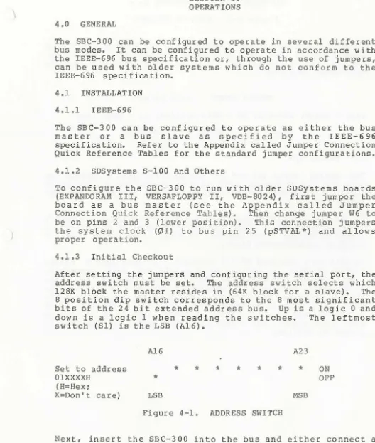
(7) /.. TABLE OF CONTENTS Subsection Number. (Continued). 'l'i tle. ) I. Page No.. SECTION II--Continued FUNCTIONAL DESCRIPTION--Continued 2.6.2 2.7 2.7.1 2.8 2.8.l 2.9 2.9.1. LINE TERMINATION SASI/PARALLEL PORT CIO SERIAL I/O ASCC POWER REGULATION S VOLT BUS OPERATION. 2-18 • 2-19 2-19 2-19 2-20 2-20 2-20. SECTION III THEORY OF OPERATION. I l j I. 3.0 3.1 3.1 . l 3.1.l . l 3.1.1 . 2 3.1.2 3.1.2.1 3.1.2 . 2 3.1.3 3.1.3.1 3.1.3.2 3.2 3.3 3.3.1 3.3.2 3.3.3 3.3.C 3.3., . 1 3.3.4.2 3.3.4.3 3.3.5 3.4. GENERAL MASTER/SLAVE MODES MASTERS PERMANENT BUS MASTER TEMPORARY BUS MASTER SLAVES SLAVE PROCESSORS SLAVE PROCESSORS AND MULTI-USER SYSTEMS BUS CYCLE OPERATIONS BUS CYCLES TEMPORARY MASTER ACCESS CYCLES SLAVE PRIORITY INTERRUPTS NON-MASKABLE INTERRUPTS MASKABLE INTERRUPTS INTERRUPT ENABLE INTERRUPT CONTROL OFF-BOARD INTERRUPT PRIORITIZATION ON-BOARD INTERRUPT PRIORITIZATION ON-BOARD INTERRUPT ARBITRATION INTERRUPT ACKNCMLEDGE MAPPER CONCEPTS. 3-1 3-1 3-1 3-1 3-1 3-2 3-2. 3-2 3-3 3-4 3-4 3-5 3-5 3-5. ). 3-5 3-6 3-6. 3-7 3-7. 3-8 3-9. 3-10. SECTION IV OPERATIONS .t.-0 4.1 .t.1.1 .t.1.2 4.1.3 .t.2. GENERAL INSTALLATION IEEE-696 SDSYSTEMS S-100 AND OTHERS INITIAL CHECKOUT SERIAL I/O. 4-1 4-1 4-1 4-1 4-1 4-2. I'.
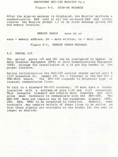
(8) TABLE OF CONTENTS. (Continued). Subsection Number. Page. Title. No.. ·SECTION V MONITOR. s.o. 5.1 s.1.1 5.2 5.2.l 5.2.2 5.2.3 5.2.4 5.2.5 5.2.6 5.2.7 5.2.8 5.2.9 5.3 5.3.l 5.3.2 5.3.3 5.4 5.4.l 5.4 . 2 5.4.3 5.4.4 5.4.5. 5.4.6 5.5 5.5.1 5.s.2 5.5.3 5.5.4 5.6 5.6.1 5.6.2 5.6.2.1 5.6.2.2 5.6.2.3 5.6.2.4 5.7. s..s. GENERAL SD MONITOR START-OP COMM.AND SYNTAX MEMORY COMMANDS MEMORY MANAGEMENT - •A• COMMAND MEMORY DISPLAY - •D• COMMAND EXAMINE MEMORY - •E• COMMAND FILL MEMORY - °F• COMMAND EXTENDED MEMORY TEST - •J• COMMAND LOCATE STRING - •L• COMMAND MOVE MEMORY - •M• COMMAND MEMORY TEST - •T• COMMAND VERIFY MEMORY - •v• COMMAND INPUT/OUTPUT COMMANDS INPUT FROM PORT - • 1 • COMMAND OUTPUT FROM PORT - •o• COMMAND PORT EXAMINE - •p• COMMAND PROGRAM CONTROL co~~ANDS BREAKPOINT - •s• COMMAND •Go• TO PRcx:;RAM - •G • COMMAND SINGLE STEP - •s• COMMAND REGISTER EXAMINE - •x• COMMAND BEX ARITHMETIC - •a• COMMAND COMMAND PROCESSING - •y• COMMAND DISK UTil..ITY COMM.ANDS BOOT OP - •c• COMMAND READ PROM DISK - •R• COMMAND WRITE TO DISK - •w• COMMAND FORMAT A DISK - •z• COMM.AND CIO INITIALIZATION AND USE ACCESSING THE CIO INTERNAL REX;ISTERS SBC-300 MONITOR AND CIO INITIALIZATION PORT B PORT C PORT A COUNTER/TIMERS ASCC INITIALIZATION PARITY ERRORS. 5-1 5-1 5-1 5-3 5-3 5-4 5-5 5-5. 5-6 5-6 5-7 5-7 5-7 5-8 5-8 5-8 5-9 5-9 . 5-10 5-11 5-11. 5-12 5-12 ' 5-13 5-13 5-13. 5-14 5-15 5-15 5-15 5-15 5-16 5-16 5-18. 5-19 5-19 5-19 5-19. SECTION VI ENVIRONMENTAL CONSIDERATIONS 6.0. 6.1 6.2. GENERAL POWER REQUIREMENTS PHYSICAL SPECIFICATIONS. 6-1 6-1 6-1.
(9) TABLE OF CONTENTS. Page. Subsection Number. ). ( Continued). 'l'i tle. No .. APPENDICES A B. c. D E. F G B I. J K L. M N 0. p. 0. SELECTED IEEE-696 SPECIFICATION SHEETS HEXADECIMAL TO DECIMAL CONVERSION STANDARD ASCII CODES EBCDIC TABLE CIO SPECIFICATION ASCC SPECIFICATION PAL16L8 SPECIFICATION PORT ASSIGNMENTS PARALLEL INTERFACES: SASI/CENTRONICS MONITOR LOCATIONS SAMPLE I/O SUPPORT CODE JUMPER CONNECTION QUICK REFERENCE TABLES DISCLAIMER LIMITED WARRANTY PARTS LIST FOR SBC-300 PARTS PLACEMENT DIAGRAM SCBEMATIC. A-1 B-1 C-1 D-1 E-1 F-1 G-1 B-1. l-1 J-1 K-1 L-1. M-1 N-1 0-1 P-1. 0-1. ). ILLUSTRATIONS Figure No •. •. 2-1 4-1 4-2 4-3. 'l'itle. BLOCK DI AGRAM ADDRESS SWITCH SIGN-ON MESSAGE MEMORY ERROR MESSAGE. Page No.. 2-1 4-1 4-2 4- 2. '!'ABLES '!'able No. •. 2-1 2-2. i-3. 2-4 5-1 5-2 5-3. Page 'l'i tle. CPU CLOCK SPEED SELECTION WAIT STATE SELECTION ON-BOARD MEMORY LOCATION IN BUS SYSTEM SELECTION JUMPER CONNECTIONS FOR BOS MASTER OPERATION SD MONITOR COMMAND SUMMARY SD MONITOR REGISTER MAP DISK FORMATS. No.. 2-4 2-9 2-12 2-19 5-2 5-10 5-14. ,,.
(10) SECTION I INTRODUCTION 1.0. GENERAL. The SBC-300 is a high performance, self-contained microcomputer system designed around the Z-80 family of micro processors. Cont r o 1 (CPU) , memory , an a extensive input/output facilities are all contained on a single printed wiring board conforming both physically and electrically to every S-100 BUS requirement as specified by IEEE-696. Operation as either the IEEE-696 Permanent Bus Master or as one of any number of slave processors on the bus is supported. The advanced design of the system allows a wide variety of function and performance option s to be selected and easily implemented by the end user in most cases by simple dip switch or jumper arrangement. In addition, the SBC-300 is available with the appropriate CPU, support, memory elements, and jumpers installed for operation at clock speeds of 4 or 6 mHz. In most cases, options are selected by the connection or disconnection of one or more jumpers; a table will show the specific jumper connections to be made for each option des i r ea. The SB c- 3 0 0 w i 11 be con f i g u r e d at th e f act or y in a manner which is likely to sui t the greatest number of users. Those requi ring different pe rformance may change option selections a s required. ). 1.1. FEATURES S-100 Bus Compatible ( IEEE-6 96). Serial, Parallel, and Counter-Timer I/O. Z-80 CPU: 4 or 6 mHz. SAS! Port. 64K Bytes of Internal RAM Plus Parity. Fully Programmable Communications Options. 2 to 16K Bytes of PROM. Dual Programmable Serial Full-Duplex Channels. Using Byte-Wide PROM System Memory Addressing to 16Mbytes 1.2. Dual Programmable Baud Rate Generators. SCOPE. This document describes the function, performance, electrical and physical characteristics of the SBC-300 single board microcomputer system and its interface to the IEEE-696 bus. For detailed description and analysis of individual integrated circuit components, the SASI port, and the IEEE-696 bus beyond what is presented here, consult the various manufacturer data books and s t andard specifications.. 1-1.
(11) ) TH IS PAGE I NTENTIONALLY LEFT BLANK. ). 1- 2.
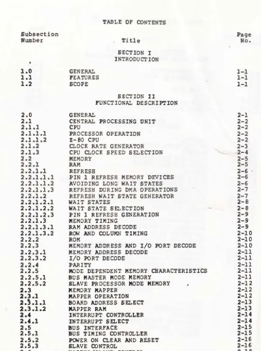
(12) SECTION II FUNCTIONAL DESCRIPTION 2. 0. GENERAL. This section provides a functional description of the basic blocks that make up the SBC-300 single board microcomputer . A block diagram of the SBC-300 appears in Figure 2-1 , and each b lock is discussed in this section. Refer to Section III for an in-depth theory of operation. The SBC-300 communicates with peripherals through one SASI/parallel and two synchronous or asynchronous serial ports. When operated as the Permanent Bus Master in acc.:>rdance with the IEEE- 696 standard, the SBC-300 controls all aspects of bus operation and provides timing, control, and status signa l s for S-100 bus operation as well as its own operation. In the slave processor mode, the SBC-300 responds to bus cycles initiated by the current bus master and/or processes data in accordance with instructions stored in the on-board ROM and RAM . It is able to communicate with the outside world via its serial and parallel ports . A slave appears to the bus as a 64K block of RAM . Data is transferred between the slave and the bus via the slave ' s on-board dual ported RAM. A slave device may request service from the bus master by generating an interrupt r equest.. AS-232. CPU i. !ADDRESS. IDATA. I. MEMORY. II. RB - 23. SER I AL. I I. 110. SASI POAT. SABI PARALLEL. I. I. S-100 BUS. II. I. INTERRUPT CONTROLLER. IMEUOA~I. I DRIVERS. M f.STER/ SLAVE. .I. CONTROLLER. I. MAPPER. I. I. I STATUS. I. Figure 2-1 . 2-1. BLOCK DIAGRAM.
(13) 2.1. CENTRAL PROCESSING UNIT. This block of the SBC-300 includes the CPU generator . The CPU of the SBC-300 is a fami l y and can be run at clock speeds selected by the appropriate conf i gur ation jumpers . 2.1.1. and the cl oc k rate member of the Z-80 of 4 or 6 mHz as of the clock speed. ). CPU. During normal operati o n, the CPU directs all aspects of data manipulation, movemen t, s torage, and r et rieval within the SBC300 microcompu ter. The CPU controls c ommunications with the outside world (serial and parallel I/O), othe r bus periph erals , and dyn a mic me mory refresh during norm al bus cycles . 2.1.1.1. Processor Operation. The function of the CPU is to get instructions from memory and perform the desired operations. The CPU accesses a location in memory and retrieves a coded instr ucti on. This instruction is decoded and then performed by the CPU . The address of the next instruction to be executed is applied t o the address lines and the instruction (OP CODE) is fetched and executed. This process is continued indefinitely or unt il the processor is stopped for some reason.. ). The system memory is used to contain the instructions for the CPU to execute and the data that is to be processed. A typical ins truction sequen ce may be to read data from a particular peripheral device, store it in a specific location in memory, and then write it out to another periphe ral. 2.1 . 1 . 2. Z-80 CPU. The Z-80 CPU itself contains many of the same functions (on a smalle r scale) as the SBC-300. There is an internal data bus for moving data to and from internal memory (registers) as well as into and out of the Z-80. The re are areas that p rocess data, co ntrol t he opera tion of the rest of th e chi p, and generat e contr ol and status si gnals tha t are re quired to control and in terf ace with things in the outside world. Registers are used within the CPU to store instructions and data . Thes e regi sters are small areas of memory which are controlled directly by the CPU Con trol (ther e is no in ternal address bus for acces sing registers) . Th e Z-80 contains 208 bits of R/W memory that are accessib le to the progr a mmer. This memory is arrang ed as eighteen 8 bit registers and four 16 bit regi sters. All Z-80 registers are construct ed o f static RAM and include 2 sets of 6 general purpose registers. These regist er s may be us ed individually as six 8 bit 2-2. ).
(14) regi ste rs or in pairs as thr ee 16 bit registers. There are also 2 sets of accumulator and flag registers and 6 special purpose registers . The act ual pr oce ssing in the Z-80 takes place in the Arithmetic and Logic Unit (ALU) which communicates with the i nternal dat a registers as well as the external data bus by way of the internal data bus. Th e ALU can perform a number of logi ca l and arithmetic operations on data contained in internal regi ster s at the direction of the CPU Control. Th ese operations include : ADD. SUBTRACT AND. OR. XOR COMPARE SHIFT L/R TEST BIT. INCREMENT DECREMENT SET BIT RESET BIT. One instructio n at a time is r et rieved from the system memory and loaded in the instr uction regi ster. The CPU Control section decod e s the instruction and generates all control s ignals necessary to execute the instruction. These signals read and write data from and to the registers, control the ALU, and control all external items as req uired by the rest of the system. Dynamic RAM mu st be refresh ed by accessing each row in the memory matrix once every 2 or 4 milliseconds, depending on the RAM type. While the CPU is busy decoding an instruction that has been fetch ed, the internal memory refresh register sends address data out on the lower port io n of the address bus along with a refresh control signal to access a row of memory. The register is incremented one and the new data sent out to access the next row of memory after every instruction fetch. As the register rolls over, the fir st row i s again accessed. As long as th e CPU is running (fetching and pe rforming instructions), the memory is automatically refreshed by the memory refresh counter . This operation is completely transparent to the system. 2.1.2 Clock Rate Generator The clock rate generator includ~s th e crystal controlled clock oscillator, the division logi c to derive the CPU clock (¢) and the 2 mHz CLOCK signal for the bus from the crystal frequency, and th e lin e driver for ¢ . The divi der sup plie s eith er a 6 mHz or a 4 mHz CPU cloc k an d a 2 mHz clock . The 6 mH z clock is derived from a 12 mHz cryst al , and th e 4 mHz clock is deri ved from an 8 mHz crystal . These rates are selected by a comb ination of the appropriate chip installed in the board and the installation of a jumper. A 74LS93 must be installed for 4 mHz operation or a 74LS92 for 6 mHz operation. This IC al so applies the proper division ratio to the crystal frequency to arrive at an output of 2 mHz for either of the two possible crystal freq uenci es that might be installed. The 2-3.
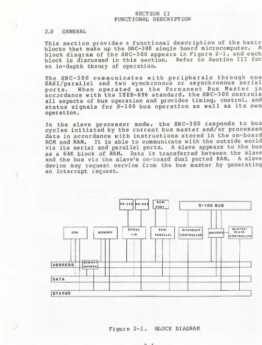
(15) bus line CLOCK must always carry a signal of 2 mHz regardless of the processor clock speed to comply with the I EEE - 696 specif ica t i on. 2 .1 .3. CPU Clock Speed Selection. The SBC-300 is configured at the factory for the processor speed spec ified, but may be reconfigured by the user for other CPU clock speeds. If the clock speed is to be increased, the speed of the CPU, peripher a ls , and memory chips must be increased as well . This requires the rem oval of the existing parts a nd installation of f aster parts in these locations. If the clock speed is to be reduced for some reason, no change of th ese units is required.. * * *. C A U T I 0 B. * * *. MULTI-LAYER PRINTED WIRIBG BOARD When reaoving parts from the SBC-300 board , ensure that the proper des oldering tools and techniques are used to prevent damage to the printed viring board surf ace and inter-layer etches.. The actual CPU clock speed is de te r mined by a combination of jumper connection s and par ts (cry st al frequency and div is ion ratio). One or both of these parts must be changed to ef fect a change of the CPU clock speed. Once these parts are in place and the appropriate speed units are installed for !Cs U46 through U48 and the on- board RAM (Table 2-1), the SBC-300 is configured for one of two CPU clock speeds. Table 2-1. Proc. Speed ( mH z). Xtal. 6. 12 8. 4. (Yl). U42 7 4LS-. CPU CLOCK SPEED SELECTION U 46 U47 Peripherals. U48 CPU. RAM Speed {ns). Z-80B Z-80A. 150 200. {mHz) . '92 '93. Z8536A Z8536. Z8531A Z8531. Delay Line (ns) 150 200. If the fastest (most expensi ve) CPU, peripheral, and memory chips are ins talled, it is recommended that the CPU clock be run as fast as is con sistent with the slowest chip on board. If the fast units are installed, there is little to be gained (sligh tly less power will be dissipated) by r unning the CPU clock at a lower than maximum speed. If the SBC-300 is to be run at a low CPU clock rate, populate the board with the slowest parts. 2-4. ).
(16) 2.2. MEMORY. The SBC-300 supports full 24 bit memory addressing in accordance with the IEEE-696 specification and may be operated in either the PERMANENT BUS MASTER or the SLAVE mode . Appropriate memory facilities are provided on board to fully exploit the flexibility and utility of the standard bus. A full 64K of dynamic RAM (64Kxl parts) with parity is installed at the factory . Any byte-wide (up to 128K) PROM may be plugged into the 28 pin socket on the board. Upgrading the on-board memory system requires removal of the existing parts and installation of the replacement memory chips. S e veral modes of refresh are available to cope with any anticipated situation that might arise on the bus. The on-board memory, as well as any memory that might be visible to the bus, can be mapped to reside in any location within the 16Mbyte range specified by the IEEE-696 S-100 standard. The 16 bit address capability of the Z-80 processor is augmented by a memory mapper which affords the Z-80 access to the entire 16Mbyte potential of the new S-100 bus standard. The basic memory block of the SBC-300 can be divided into several subsystems: RAM, ROM , MEMORY ADDRESS AND I/0 PORT DECODE , and PARITY. These subs ystems are required to support the 2 intern al memo ry syst e ms (RAM and ROM) and to e nsure compatibility with th e bus sta ndard and the v arious other blocks on the SBC-300 . 2 .2 . 1. RAM. The RAM devices that are installed prior to shipment allow pin 1 refresh and are selected so that their speed is consistent with the CPU clock rate. Upgrading the on-board RAM requires r e placement of the set of memory IC chips and the possible connection of a few jumpers to select the proper wait states . The only constraints are that the RAM speed be compatible with the CPU clock rate and that the refresh requirements are met (acceptable device numb e rs for replacement appear - in the Parts List Appe ndix) . CPU clock rate considerations are discussed above in the CPU subsection and the refresh restrictions are covered below. The RAM subsystem includes a latch for data out and line drivers for interface to the bus as well as several small blocks and functions which work together to allow the RAM to perform properly and interface with the rest of the system . These items are: refresh, refresh wait state generator, and memory timing.. 2-5.
(17) 2.2.1 .1. Refresh. Any memory device equivalent or similar to the items noted in the Parts List Appendix may be installed in place of the existing RAM devices to increase capacity , replace failed parts (all chips in the array should be of the same type), or satisfy any other particular need of the user. There is, however , one refresh restriction which must be observed:. * * *. C A U T I 0 N. ). * * *. REFRESH IS NOT SUPPORTED DURING LONG BUS WAIT STATES IF RON-PIR 1 REFRESH PARTS ARE IBSTALLRD There are 2 easy solutions to the situation. One is to use pin 1 refresh memory devices in the on-board memory system, and the other is to make sure that items which might cause a long wait state for the processor are never attached to the bus. 2 . 2 .1.1.1. Pin 1 Refresh Memory Devices. Industry standard 64K dynamic RA M devi c es are refreshed by addressing eac h ro w of t h e sto rage ma t ri x within 2 milliseconds . Thi s is call ed Ro w Ad d r e ss Strobe or RAS refresh . Pin l i s not connec t e d to the IC die (it is a nonconnect) and the only method of re fr esh is through the refresh address access c ycle gene r ated el s ewhe re.. ). The Z- 80 is rather unique among microprocessors in that it has an internal 7 bit address counter which generates memory refresh cycle addresses after every OP CODE fetch. If the processor is stopped (in a wait state) for an ex t ended period of time , there will not be an OP CODE fetch in time to refresh the memory . If this happens, the data in the memory devices becomes uncertain and cannot be used. Memory devices wi th pin 1 refresh , how e ver , allow refresh to be performed by . an additional procedure . There is logic on the SBC-300 that detects long wait ~tates. This logic then generates a refresh cycle which is applied to pin 1 of the appropriately equipped memory devices. The pin 1 refresh cycle is repeated at the proper interval until the processor is running again and pin 1 refresh is no longer needed to maintain the memory. The only time this cycle is implemented is during wait states where the CPU is stopped for excessive amounts of time. 2 .2 . l.l.2. Avoiding Long Wait States. The other method of preventing loss of memory data during long wait states is to never install any device on the bus that might generate a long wait state. Sources of long wait states 2-6. ).
(18) include items such as polled I/O disk controllers. These devices use wait sta tes to transfer data into the system memory. If, for example, the processor directs the disk controlle r to read a sector into memory and the sector requested has just passed the heads, the controller must then wait (which means that the CPU must wait} until that sector comes around again to retrieve the data. This can take as long as 150 ms, which is 148 ms too long if the memory content is to remain valid. The Versaf loppy II disk controller is an example of a polled I/O devi.ce that uses a wait state to transfer data to and from the memory. OMA devices such as the Versaf loppy III disk controller do not cause long wait states for data transfe r and so are safe to use without pin 1 refresh memory devices . 2. 2.1.1.3. Refresh During OMA Operations. During a OMA operation, where the SBC-300 is the permanent bus master but has relinquished control of the bus to a OMA device, the SBC-300 generates standard memory refresh cycles from bus activity. As a result, even if there is a DMA controller transferring data into another memory board on the bus, SBC-300 memory is preserved due to its self-generation of refresh cycles. Depending on the design of other memory boards that might be installed on the bus, this self-generated refresh cycle might take care of memory on the bus as well as on the SBC-300 board. Older designs (such as the EXPANDORAM II and III} can be refreshed in this manner, while newer designs (EXPANDORAM IV} support this procedure as well as several others during DMA transfers. These boards, which might be used with other processors (no other processors generate memory refresh cycles}, take care of the refresh for on-board memory devices themselves and do not care if the bus master processor is stopped or not. With that type of design, when refresh is not obtained from the bus master processor, the memory board generates cycles for itself. The bus ·is held off by the memory board until it is finished so it will not be busy· with a refresh cycle at the moment its services are required by the bus. Refresh occurs independently of all other activity on the bus, and memory is thus immune to long wait states. There is usually a jumper selected option on these boards, however, which allows refresh to be forced at certain times. 2.2.1.2. ). Refresh Wait State Generator. The refresh wait state generator perfor ms 2 func tion s. It simultan eously generates the pin 1 refr esh signal and holds the wait line low. The wait line is held low only during the refresh cycle; so if the long wait state which activated the. 2-7.
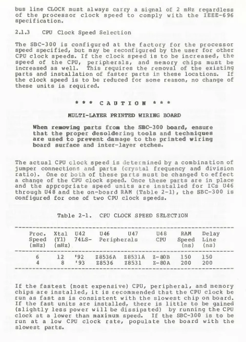
(19) pin 1 refresh cycle goes away, the pin 1 refresh cycle will not be interrupted until the refresh is complete. 2.2.1.2.1. ). Wait States. Wait states are ordered by devices a tta ched to the S-100 bus and by the SBC-300 itself. Generally wait sta tes are called to hold up the processor because the CPU runs faster than some peripheral devices are capable of responding. To ensure that valid data read from memory has settled on the data lines befo re th e processor tries to use it, or to prevent the processor from removing the addres s and data from those lines before a write cycle is complete, the processor is stopped for a period of time until it is safe to proceed. The wait state is implemented by pulling down the WAIT* line to the processo r. The CPU checks this li ne on the falling edge of the clock during clock cycle T2 and, if it finds that the WA IT* 1 in e is act i v e , it s us pe n d s a 11 pr o c es s i n g th at might have occurred during the next clock cycle. This creates a wait state. The CPU will continue to create wait states as long as its WAIT* line is held low . This line (WAIT*) is cont rolled by the wait state generator. It can be triggered by the wait state generator (jumper W3; see Appendix cal led Jumper Conne c~ i on Quick Reference Tables) when lines indicat in g an OP CODE or memory operation become active. This memory operation tri gger produces a synchronous wait state of exactly 1 clock period. A device on the bus can trigger a wait state of any duration beginning at the next falling edge of the clock by pulling and holding down either of 2 lines on the bus (RDY and XRDY) . An d fin ally, the refresh wait state generator can cause a wait state to hold off the processor while it applies a refr esh cycle to pin 1 of the on-board RAM. The RAM cannot be written to or read from during refresh, so the processor and bus must be prevented from trying to use the RAM until refresh is complete. 2.2.1.2.2. Wait State Selection. There are 3 modes of memory operation wait sta te generation possible as selected by jumper W3 (Table 2-2) . If the Ml mode is selected, a wait state is generated each time the processor fetches an OP CODE from memory. A wait state will not be generated during a normal memory access because the memory is fast enough to respond to the processor between clock T states. During OP CODE fetches, however, the CPU must refresh the on-board RAM after the read, so a wait stat e is generated to allow this refresh to be completed before things continue. If the MREQ* option is selected, a wait s tate is generated during both OP CODE fetches and normal memory accesses. This allows slower memory devices to be used with a faster processor; the processor is held up during a memory read from the slow memory but operates at full speed otherwise. 2-8. ).
(20) ). If no memory option wait state is selected, then no wait states are generated during memory operations. Table 2-2. Wait Selection Ml* MREQ* None. 2.2.1.2.3. WAIT STATE SELECTION. Wait State Jumper W3-2 to W3-3 W3-l to W3-2 None. Function l wait state during OP CODE fet che s l wait state during memory accesses No waits inserted. Pin l Refresh Generation. During long wait states, the CPU is stopped. This means that there will be no RAS refresh cycles from the processor to maintain the memory. If the processor is stopped for more than approximately 2 msec, the content of the memory will no longer be valid. To prevent such loss of data, the refresh wait state generator provides pin 1 refresh cycles to the RAM whenever the CPU is in a wait state. This causes a wait state to be generated in order to prevent the CPU from accessing the RAM during refresh. 2.2.1.3. Memory Timing. Memory timing is basically concerned with restructur ing the address information that appears on the internal addr ess bus into a form that is compatible with the memory devices and then applying that data to the RAM chips. These 2 functions are implemented by the RAM address decode and the row and column timing areas. 2 .2 .l.3 .1. RAM Address Decode. The RAM address decode is very simple . It serves to interface the RAM chip address lines to the SBC-300 internal 16 bit address bus. This is required because in order to fit into a standard 16 pin package, large capacity memory devices hav e only 8 address lines. The 16 bit address on the bus is broken into two 8 bit bytes and applied first one and then the other to the 8 address lines of the memory chip array. The two halves of the address are referred to as the row and the column address. Each pair of row and column addresses defines a unique storage location within the storage matrix of each memory devic e. This is th e same addressing scheme that was developed for magnetic core memories.. 2-9.
(21) First the row address portion of the information on the address bus is applied to the memory array address lines and then the row enable line (RAS strobe ) to the me mory dev ice arr ay is activated. Nex t the column address por t ion of th e information on t he address bus lines is applied to the same memory arr ay addres s lin es and then the column enab le line (CAS strobe ) is activ ated . This pro cedure loads the 16 b it address of the desired location into the memory device where it is internally de coded to specify a unique lo c a ti on in the storage array.. ). There are specific intervals of time which must elapse between each segment of the addressing operation (enables, settling time, change between row and column address, etc.). The row and column timing area is responsible for ge neratio n of these intervals . 2.2.1.3.2. Row And Column Timing. The memory devices require a time interval between the different parts of the addressing operation. A delay l ine with multiple taps provides these i n tervals. A pulse applied to the input appears at each successive tap a specific time after it appears at t he prev i ous tap (or the input, if the first tap is being con si dered) . Devices and lines connected to these taps a re therefor e ac ti v ated sequential ly with specific time int e rvals inbe tween. This area also c ont ains logi c which, when a ct i vat ed by t h e signals from t he delay li n e , contr ols all as pect s of RAM reads and writes. 2 . 2.2. ). ROM. A 28 pin socket on the SB C-300 board allows any of several byte-wide (2Kx 8, 4Kx8, etc.) ROMs to be plugged in. The Parts List Appendix shows compatible device type numbers . The ROM installed before shipment includes the Monitor firmwar e and the system BIOS. Ther e is empty space in the ROM that can be used for any purpose the user desires. However, the user is responsible for programming the ROM with additi o nal code. The RO M portion of the on-board memory occupi es the first 64K segment of th e total 128K block even though a relatively small device might be i nstalled in the socket. Because t he ROM is invisible to the bus, the SBC-300 appears to other items on t he bus as an ordinary 64K block of RAM when in the slave mode. 2.2.3. Memory Address And I/0 Port Decode. The on- board address and p ort decoding is handled by a combination of the Zilog 8536 Counter Input/Output chip (CIO) ,. 2-10. l.
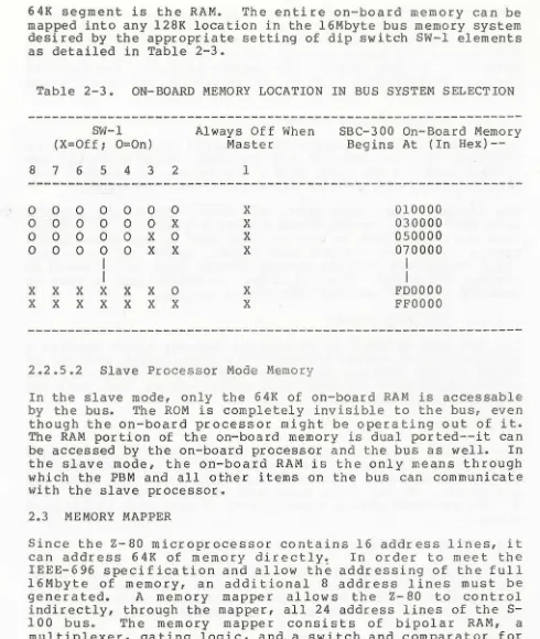
(22) a PALl (U28) and a decoder chip. The CIO generates a signal {BOOT) which is used by the PAL in conjunction with other timing signals to decide whether the processor is talking to RO M, RAM or off-board memory . When an I/O addres s is being generated, the PAL inhibits the enables to memory devices, and the port decoder (U57) enables the particular I/0 device being addressed. 2.2.3.l. Memory Address Decode. The memory decoder generates 4 sign als which ar e used to determine what the SBC-300 is addressing. These 4 signals are created within a PAL (U28) from a combina tion of standard Z- 80 timing si gnals and on-board hardware/software switches. The 4 signals are PRO M ENB*, RAM ENB*, RDOFF* and GORAM*. PROM ENB* is the on-board ROM enable signal. It is created when the BOOT signal is active. RAM ENB* is the on-board RAM enable signal for the ROM data latch. RDOFF* is the signal which determines that the present memory cycle is o ff board on another 696 board. The 4th signal is GORAM* and is used to generate the RAS* and CAS* RAM timing s ignals . 2.2.3.2. ). I/O Port Decode. The I/O port decoder is an address decoder which enables a particular I/O device whenever i ts preselected address is found on the address bus. The I/O decoder generates the enable signals for the ASCC, CIO, memory mapper, SAS! Port and the ATTEN inte r rupt bit . 2 .2.4. Parity. The SBC-300 generates and checks odd parity in it s on-board RAM. The parity checker generates 2 parity error signals for use by the on-board processor and, if in the slave mode, the bus master. Parity error detection is enabled by jumper Wl44. The on-board parity error signal is also sent to CIO port c bit 1. 2.2.5. Mode Dependent Memory Characteristics. Some memory characteristics exhibited by the SBC-3 00 change according to the SBC-300 mode selected. Th e SBC-300 may be operated as either the Permanent Bus Master (PBM) or as a slave proces sor in accordance with IEEE- 696 specifications. 2.2.5.1. Bus Master Mode Memory. In the PBM mode, the SBC-300 occu pi es 128K of the syst em memory space. The 1st 64K s egment is PROM (even though there may be only an 8K PROM installed in the socket), and the 2nd ). lpAL - Programmable Array Logic MMIR 2- 11.
(23) 64K segment is the RAM. The entire on-board memory can be mapped into any 128K location in the 16Mbyt e bus memory system desired by the appropriate setting of dip switch SW-1 elements as detailed in Table 2-3. Table 2-3 .. ). ON-BOARD MEMORY LOCATION IN BUS SYSTEM SELECTION. -------------------------------------------------------------SW-1 Always Off When SBC-3 00 On-Board Memory (X=Off; O=On). Master. 8. 7. 6. 5. 4. 3. 2. 0 0 0 0. 0 0 0 0. 0 0 0 0. 0 0 0 0. 0 0 0 0. 0 0. 0. Begins At (In Hex)--. l. -------------------------------------------·------------------x. x 0 x x. x x x. 010000 0 3 0000 050000 070000. x x x x x x 0 x x x x x x x. x x. FDOOOO FFOOOO. x. I I. 2.2.5.2. I I. Slave Processor Mode Memory. ). In the slave mode, only the 64K of on-board RAM is accessable by the bus. The ROM is completely invisible to the bus, even though the on-board processor might be operating out of it. The RAM portion of the on-board memory is dual ported-- it can be accessed by the on-board processor and th e bus as well. In the slave mode, the on-board RAM is the only means through which the PBM and al l other items on the bus can communicate with the slave processor. 2.3. MEMORY MAPPER. Since the Z-80 microprocessor contains 16 address lines, it can address 64K of memory directly ~ In order to meet the IEEE-696 specification and allow the addressing of the full 16Mbyte of memory, an additional 8 address lines must be generated. A memory mapper allows the Z-80 to control indirectly, through the mapper, all 24 address lines of the S100 bus. The memory rnappe r consists of bipolar RAM, a multiplexer, gating logic, and a switch and comparator for selecting which 64K block of system memory the board occupies. 2.3.1. Mapper Operation. The upper 4 bits of the Z-80 physical address lines (Al2-Al5) are applied to the address inputs of the memory mapper RAM to determine which location within the mapper will be accessed 2-12. ).
(24) and output to the extended address bus (Al2-A23). The mapper is accessed as 1/0 port 71H for purposes of updating the stored address. The memory ma pper is bypassed during 1/0 operations and during accesses to the on-board EPROM. During these periods the upper 4 address bits are passed directly to the logical address bus. 2.3.1.1. Board Address Select. The board address select consists of a dip switch and a comparator containing internal 20K pullup resistors. One set of inputs to the comparator is tied to address bus lines Al6 to A23 on the S-100 bus side of the on-board address line drivers . The other set of inputs to the comparator is connected to the board address select dip switch SWl . Once the starting addr ess of the board is decided, SWl is set to reflect the board starting address. The 8 elements of SWl are capable of defining 256 different 64K boundaries anywhere in the l 6Mb yte range (2 8). The boundaries can be thought of as boundary 0 (beginning at addr ess 0) through boundary 255 (beginning at address 16,711,680). The user selects the binary equivalent for the decimal number of the desired boundary by means of the 8 el ements of SWl. The comparat or constantly checks the state of each of the address lines to which it is connected against the setting of the address sel e ct switch SWl . When a match is found, the compar ator indicates the match by activating its output line. This output is used elsewhere on the board to indicate that the on-board 64K of RAM is being addresse d. Care must be taken to ensure that no 2 boards attached to the bus have memory that is set to the same starting address. 2 .3 .1 .2. Mapper RAM. The memory mapper RAM is composed of a 16xl2 bit bipolar highspeed static RAM matrix (three 16x4 devices). The upper 4 bit address lines (Al2-Al5) from the Z-80, when applied to the mapper RAM addre ss input lines, select one of sixteen 12 bit data words . This 12 bit word is applied to the upper 12 bits of the S-100 addr ess bus (Al2-A23). These 12 address lines f r om th e mapper , a 1 on g wit h the 1 2 1 ow e r add r es s 1 in es f r om the CPU, create 24 real address lines that are driven out onto the bus, al lowing access to the entire l 6Mbyte address range by the z- 80 . The 12 bits of da ta to be loaded into the mapper RAM appear on the 8 data lines (D0-07) of the data bus and 4 lines (AS-All) of the address bus of the SBC-300 board. Just after power up the monitor firmware loads the mapper RAM with initial data by applying the appropriate data to the input lines for each address and selecting each of the 16 locations sequentially with Al2-A15 of the on-board address bus. ' 2-13.
(25) Once t he operating system is in control, it can change the content of the mapper RAM at any time as required. Application programs can, in certain circumstances, change the mappe r RAM content dynamically as the program exe c utes, al l ow i ng immediate access to the entir e system memory. 2 .4. ). INTER RU PT CONTROLLER. The SBC-300 provides service for the Non-Mask a ble Interrupt a n d the 8 vec tored in terrupt lines fro m the S- 10 0 bus as well as th e interrupts from the 2 serial communicati on ports . The interrupt controller prioritize s on-board interrupt requests and the vectored in t errupt lines from the bus, generates the lea st signifi c ant 8 b i ts of t h e interrup t vector, and s tarts the int errup t c ycle. An i nte rrupt can also be gene rated in re spon s e to th e sta tu s of sev eral other lin e s on the b us ( j ump e r s e 1 e ct ab 1 e by the use r } to a 11 ow spec i a 1 f e at u r es t o be implemented. 2 . 4. 1. Interr upt Selec t. An area of the SBC-300 board is reserved for the user to install jumpers to connect any of several lines from other places on the board as well as the S-100 bus to the NMI and vectored interrupt lines. If the SBC-300 is configured to be the bus master, th ere are 2 li n es from the bus that are considered input s (PWRFAIL and ERROR). As a slave processor, there are 7 jum per s that might be in stal led in order to put the on-board par ity error and at tention lines out onto the bus as vectored interrupts.. ). As a master, the power failure line might be jumpered to the NMI and the parity error line jumpered to one of the vectored interrupt lines so that if devices on the bus detected these co n d it ions, t h e bu s master processor wou ld be immed i ately noti fi ed and coul d pr oceed a ccordingly. As a slave, the on-board attention line could be jumpered to any of 6 vectored interrupt lines on the S-100 bus. This would allow the interrupt controller on the bus master to easily determine which slave was requesting the interrupt and then generate the appropriate service routine vector. This procedure limits the number of slaves on the bus to 6. In situation s where there ar e more th a n 6 s l aves on th e bus, al l sl ave atte ntion l ines co ul d be jumpered to o ne or a few inte r rupt lines on the bus. Then the bus master CPU can poll the slaves to de t ermine which one requested the interrupt as part of the interrupt service routine. All slave parity error line s are u sua lly j umpered to a sing le interr up t line (VIl), and t he bus ma ster CPU can pol l the sl aves to deter mi ne the loca ti on of the error.. ). 2-1 4.
(26) 2.5. BUS INTERFACE. The IEEE-696 S-100 bus standard specification describes a universal bus that can support a wide range of processors rath e r than just a pa rticular proc es sor or family of processors. Signals required to be on the bus were deemed to be the best compromise between ease of implementation and util it y. The bus is configured to allow the widest range of processors the mo st flexibility pos s ible without being completely incompatible with existing systems. Because the bus is a unive rsal design, it is not expect ed that all status and control signals from a particular processor will be directly applicable to the bus. Nor will all signals on the bus be directly compatible with the requirements of a particular CPU. All processor manuf act u rers have slightly different ways of accomplishing th e sam e task with their ma ch ine s . Signal names, polarity, phase, and timing might vary radically from one CPU to another even though the bottom line of what gets accomplished is identical . As a result of all thi s , some of the signals from the Z-80 CPU on the SBC-300 must be processed a little before they can be applied to the bus, and some signals on the bus must be proces sed a little before the Z-80 can understand th em. This is t h e task of the bus interface. ). The bus interf a ce block consis ts of several smaller blocks, each one handling a portion o f the job. As bus master, the SBC-300 supplies all timing and control signals on the bus. The bus timing controller uses signals from the CPU and other areas of the bo ard to synthesize the signals required to run the bu s . The Power On Clear (POC) and RESET area si mply handles power clears and resets when the SBC-300 is in either mode . When the SBC-300 is operated in the slave mode, the slave control area tran sl ates the bus signals into a for m that can be understood by the Z-80 so that the SBC-300 can be pr oper ly synchronized to the activity on the bus. 2.5.1. Bus Timing Controller. As bus master, the SBC-300 must supply all timing and control signals for the bus. The IEEE-696 s pec if ica tion calls for a bus that runs a lmo st everything off th e rising edge of th e clock. The Z- 80 runs almost everything off the fa lling edge of the clock. The solution is to invert the clock and signals out of the CPU and to del ay so me si gna ls to get the proper timing relationships for the bus. Ot her si gna ls tha t the Z-80 does not provide directly are derived from the signals th at it doe s generate. The status and control signals that must be applied to the bus when the SBC-300 is operated as bus master are derived fr om 2-15.
(27) the status and control signals from the Z-80 CPU. Through combinational logic (gates), bus standard equivalent signals are construct ed from those avai lable from the CPU and appl i ed to the bus. Clocked logic allows the timing relationship of signals to be adjusted t o meet the bus specifica tio n.. ). Signals that need to be delayed or have the timing adjusted are de rived from a chain of flip-flops. As the input propagates through the chain, different signals are picked off at t he appropriate poi nts an d sent out to the bus. Thes e signals have a constant and predictable relationship to each other in time and mat ch the signal function and timing relationships req uired by the IEEE-696 bus specification. The address bus is deriv ed from two so urces. The low order bits {AO-All) are taken directly from the Z-80 , while the high bits {Al2-A23) are derive d from the memory mapper. The low order addr es s bits are driven directly by the Z-80 CPU and will not hold on the bus as long as the high bits. Therefore, care should be tak e n to insure that no co nflict is created by the short hold t ime on the low order addres s bit s . In the slave mode, the SBC-300 must not apply any of the on- board status and control signals to the bus. The bus timing controller causes the output of the gated line drivers for these signals to become a hi gh impedance when the master mode is selected, ther eby preventi ng problems on the bus. 2.5.2. Power On Clear {POC) And RES ET. ). This area performs a few simple tasks. In the master mode, it holds down the RESET line on the bus until the power has come up and stabilized. This makes sure that all items on the bus (including the SBC-300) get a RESET signal after the power lines are up f ar enough for the devices to fully reset. Otherwis e, there may be random data in memory ce lls and regi sters that could cause tr ouble if they are not clear ed out before normal oper ation. The RESET signal is applied to the POC and SLVCLEAR lines on the S-100 bus l ine only when enabled as a master. The RESET line is also usually connected to some sort of mechanical momentary switch which is accessible to the operator for manual resets. As a slav e processor, the SLVCLEAR and RESET line s ar e monitored a nd act ed upo n inst ead of driv en. When the bus master sends o ut a SLVCLEAR signal on the bus, the slav e processors o n t he bus decode this signal as an on-board RESET and reset. 2 . 5.3. Slave Cont rol. The same bus signa ls which were derived, inverted , and/or time shifted from the Z- 80 before they wer e applied t o the bus by 2-16. ).
(28) the SBC-300, acting as bus master, must be decoded by the SBC300, acting as a slave processor on the bus, before they can be understood by the SBC-300. The slave control area takes care of this task. Combinational logic elements (gates) an d a Programmed Array of Logic (PAL) device are used as a decoder to condense many of the status and control signals on the bus down to a few signals that are meaningful to the SBC-300 and the on-board z80. Th i s requ i res that some signals be inverted and/or shif ted in time . Al 1 the timing signals that the on-boa rd CPU would norma lly generate for the on-board memory come from the bus during commur.ication with the slave. Normally the slave is running free with its CPU controlling all aspects of it s operation . But when it has to communicat e with the bus (through the memory), the bus must control the memory so that everything on the bus will be compati ble and synchronized to the bus universal tim i ng. The slave control logic accomplishes this. Because slave control logic is required to interface the slave to the.bus during memory transfers, the slave's memory does not appear (respond) exactly as just another boa rd of fast memory. There is an appreciable propagation delay through the several layer s of decoding in th e slave control area before the appropriate signals are appli e d to the on-board memory. The slave control area contains a wait state generator that sends an adjustable number of waits to the bus master CPU to hold things up until the slave decoding logic and memory systems hav e had a chance to settle and respond. The wait state generator is simply a counter that holds down the RDY l i ne on the bus until it has counted a specific number of cycles from the bus clock. The number of wa it s sent to the bus master CPU is selected by jumper . A jumper (Wl3) selects from 0 to 5 waits to be sent to the master during the slave memory cycle. If the re is no jumper installed, ther e will be no wait states sent during a memory cycle to the slave. The number of waits that should be sent is dependent on the processor clock speed of the bus master and how fast the rest of the memoTy in the system runs. Th e bus master inserts waits into an ordinary memory access, the number depending on the speed of the memory installed. The num ber of waits needed to be inserted by the sl av e is in addit ion to the waits generated by t he master du ring an ordinary memory access. In t h e master mode, the en tire slave control area is d isa bled because as the master the SBC-300 is supplying the status, timing and control signals to the bu s in stead of receiving them.. 2-17.
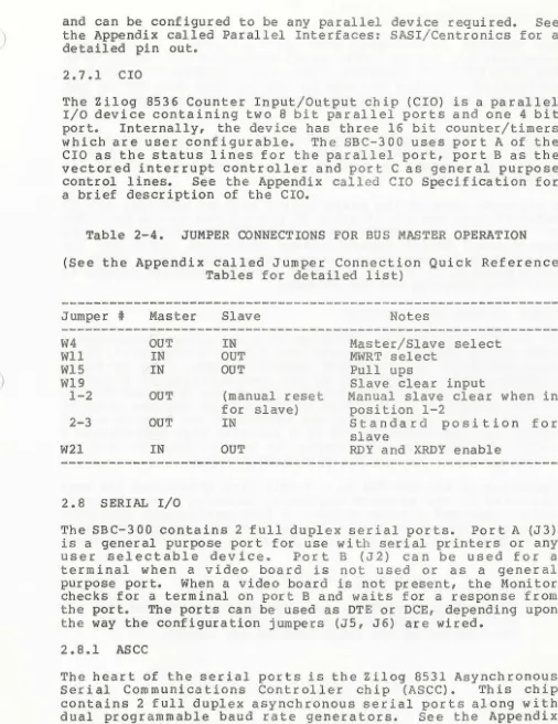
(29) 2.6. MASTER/SLAVE CONTROL. The IEEE-696 S-100 specification allows for the connection of 3 main types of devices to the bus . There must be exactly 1 Permanent Bus Master (PBM) on the the bus at all times. Up to 16 Temporary Bus Masters (TBM) and any number of bus slaves are allowed on the bus (short of the 22 maximum slots called for in the specif ica ti on).. ). The SBC-300 may be operated as either the PBM or a slave processor . There is a significant difference between one mode and the other in the way the SBC-300 operates and interfaces to the bus. These differences are effected by logic on the SBC-300 board responding to the mode selection jumpers and switc h . 2.6.1. Master/Slave Select. The main diffe rence in the activities of an SBC-300 operating in the master mode and the slave mode is that in the master mode, the SBC-300 puts status , timing , and control signal on the bus, while in the slave mode, it is controlled by those signals on the bus. In order to accomplish the necessary changes, a single hardware jumper (W4) is used to tell the CPU whether the board is a master or slave. In the master mo de , the board ignor e s the status, timing, and control signals on the bus and arr a nges to drive these lines on the bus inst ead. In the sl ave mode, the drivers are disabled and the decoders ar e enabled so that the signals on the bus control the slave. 2.6.2. ). Line Termination. The IEEE-696 bus standard provides that pull up resistors for cert ai n lines on the bus shall reside either on the bus (mother board) itself or on the PBM. Since the SBC-300 can be operated either as a PBM or as a slave processor, there is a means of providing the pull up resistors for the bus lines that require them when in the master mode (if the bus does not have them). A group of jumpers must be installed if the SBC300 is to provide the pull up resistors for the bus. If the SBC-300 is not to supply this pull up function or is operating as a slave processor, the se jumpers are to be removed. Table 2-4 shows the line termination jumpers. 2.7. SASI/PARALLEL PORT. The SASI/Parallel port is an 8 bit parallel data port along with 8 status lines. The data port is a bi-directional 8 bit port l ocated at I/O address 70H. The 8 SASI con t rol line s are controlled by the CIO port A, which is addressed as I/ O port 7AH. The port is available to the user through connector J4 ). 2-18.
(30) and can be configured to be any parallel device required. See the Appendix called Paral lel Interfaces: SASI/Centronics for a detailed pin out. 2.7.l. CIO. The Zilog 8536 Count er Input/Output chip (CIO) is a parallel I/O device co n tainin g two 8 bit parallel ports and one 4 bit port. Internally, the device 0as three 16 bit counter/timers which are user confi gura bl e. The SBC-300 uses port A of the CIO as the status lin es for th e parallel port, port B a s the vectored interrupt controller and port C as genera l purpose control lines. See t h e Appendix called CIO Specification for a brief description of the CIO. Table 2-4.. JUMPER CONNECTIONS FOR BUS MASTER OPERATION. (See the Appendix called Jumper Connection Quick Reference Tables for detailed list) Jumper #. Master. W4 Wll Wl5 Wl9 1-2. OUT. IN. IN. OUT OUT. OUT. 2-3. OU T. (manual reset for slave) IN. IN. OUT. IN. W21. 2. 8. Slave. Notes Master/Slave select MWRT select Pull ups Slave clear input Manual slave clear when in position 1-2 Standard position for slave RDY and XRDY enable. SERIAL I/0. The SBC-300 contains 2 full duplex serial ports. Port A (J3) is a gener al purpose por t for use with serial printers or any user selectable device. Port B {J2) can be used for a term inal when a video board is not used or as a general purpose port. When a video board is not present, the Monitor checks for a terminal on port B and waits fo r a respon se from the port. The ports can be used as DTE or DCE, depending u pon the way the configuration jumpers (JS, J 6) are wired. 2.8.l. ASCC. The heart of the seri al ports is the Zilog 8531 Asynchro nou s Se r i a l Communications Controller chip (ASCC). This chip contains 2 full dupl ex asynchronous ser ia l ports along with dual programmable b aud rate g ener ators. See the Appendix called ASCC Specification for the programming model.. 2-19.
(31) 2.9. POWER REGULATION. The SBC-300 is equipped with an on-board 5 volt linear regulator for use on 8 volt power busses in accordance with the IEEE-696 S-100 standard. The regulator provides a tightly controlled 5 volts for use by the various devices on the board and is immune to minor fluctuations of the 8 volt power b us .. ). If 5 volt operation is required {instead of the normal 8 volt operation) and an adequate source of well regulated 5 volts is availab l e, a jumper connection will configure the SBC-300 for 5 volt operation. A s epara te a r e a of t he p ower sup pl y section prov i des +/- 1 2 v olts DC f r om the +/- 1 6 volts DC power lines on the bus . The +/- 12 vol t s is used on the SBC-300 board only by the Asynchronous Serial Communications Controller (ASCC) for the standard RS-232 communication protocol. Very little power is dissipated in th is area, and so a zene r stabilized supply is more than adequate for the purpose. 2.9.1. 5 Volt Bus Operation. If the SBC-300 is t o be install ed o n a bus using a regulated 5 volt power suppl y to opera te t he 8 volt S-100 lines (this deviates from the IEEE-696 s peci f ication), the on-board regulator may be b ypassed b y th e installation of a jumper between the input a nd the output p i ns of the regulator device. If all items to be attached to the system bus are able to operate with a 5 volt power bus instead o f the 8 volts called for i n the specification and if a suitable high performance 5 volt regul a ted power supply is available, it may be a dvantageo us to operate the system on 5 volts. Operati on of t h e SBC-30 0 on a 5 v ol t line eliminates the heat generated by the on-board regulator, allowing a system to be safely operated without a fan . A high performance regulator (such as a switching regulator) for the bus dissipates little or no heat itself and provides generally superior regulation.. * * *. C A 0 T I 0 N. * * *. The on-board regulator must reaain in place when the SBC-300 is operated on an 8 volt power bus, or destruction of the logic devices may result.. 2-20. ).
(32) SECTION III THEORY OF OPERATION. ). 3.0. GENERAL. This section covers the general theory behind the subdivisions of the SBC-300 and the basic requirements of the IEEE-696 bus specificati on. For detailed information about the IEEE-696 specification , the user needs to obtain a copy of the specification from IEEE as it cannot be reproduced in full in this manual. 3.1. MASTER/SLAVE MODES. 3 .1. 1. Masters. There are 2 types of bus masters, permanent and temporary. Each serves a different purpose in the system from the other. The Permanent Bus Master (PBM) is a processor type device that controls the bus and the system, while the Temporary Bus Master (TBM) is usually a DMA device such as a disk or tape controller that obtains control of the bus from the PBM from time to time for the purpose of transferring data to or from the PBM or any slave on the bus. The acting bus master (permanent or temporary) may initiate bus cycles and, if it is the PBM, may grant control of the bus to a TBM on the bus. 3.1.1.1. Permanent Bus Master (PBM). As the PBM, the SBC-300 directs all bus activity within the system, driving all data, address, status, and control lines of the bus in accordance with the IEEE-696 bus standard. In this mode, the SBC-300 may utilize any resource that might be attached to the bus including system memory, any I/O device such as a disk controller or a multiple port I/O card, keyboard and video boards, and any slave processor on the bus. Control of several lines on the bus is retained by the PBM whether it has· cont rol of the bus ·or not. These signals include both clocks, the Power On Clear (POC), and the memory write line and are always controlled by the PBM to avoid timing and synchronization problems with the other items on the bus. 3 .1.1.2. ). Temporary Bus Master (TBM). A TBM is a device on the bus that may request control of bus from th e PBM to condu c t some business that requires use of the bus. When a TBM gains control of the bus, becomes the acting bus master until it returns control to PBM. The TBM does not generate all possible bus cycles does it generate all signals required to drive the bus.. 3-1. the the it the nor It.
(33) may not grant control of the bus to anoth e r TBM nor accept an interrupt request. TBMs acqui re control of the bus, conduct as much busin ess as required , and return control of the bus to th e PBM. Disk and tape cont ro l lers are examples of devices that are considered TBMs . 3.1. 2. Slaves. Th e SB C-300 may be co nfigured as a interface d to the bus as a bus slave . slaves are slave processor s.. slave . proc essor and However, not al l bus. A slave on th e bus respond s to bus cyc les initiated by the acting bus mast er. The slave constantly monitors the bus and, if addressed during a particular bus cycle , accepts the data it finds on the bus data li nes or applies data to the lines as directed by the control signals present on the bus. At the comple tion of the bus cycle, the slave resumes its regular activity if it is a slave processor or some similar device, or waits for the next bus cycle if i t is a memory board or other unintelligent device. The slave appears to the bus as sim p ly another block of memory. Each sl ave only takes up a slot on the bus a nd a block of memory in the map. The location (address) of the slave in the mem ory map is selec t ed on the slave board by means of a switch. Slaves can be added to the system until there are no more available slots on the bus or blocks in the memory map. 3.1.2. 1. Slave Processors. In the slave processor mode , the SBC-300 operates exc lusively out of on-board memory and may ut ilize any resour ce that i t can access through any means except the S-100 bus (serial ports and the SAS! inte rface). Unless addressed during a bus cycl e , the slave processor operates independently of most li nes on the bus. The acting bus master may communicate with the slave processor only through the slave processor RAM which is dual ported. As a slave proc essor, the S BC-300 may not initiate a bus cycl e, and the on ly way it can access the bus ma ster is if it pulls down an interrupt, wait, or error line to get the attent ion of the bus master in response to some condition on the board. 3.1.2.2. Slave Proces sors And Multi -User Systems. Slave processors on the bus spread the intelligence and proce ssing power around, allowing high performance mult i-u ser and/or multi-tasking systems to be easily configured on the S100 bus. Each slave p rocessor runs at fu ll speed regard les s of activity on the bus or in other processors attached to the 3- 2. ).
(34) bus. The only time bus activity impacts a part icula r slave proce ssor i s when it must in ter rup t the PBM to access some shared resource (hard disk, tap e controller, etc.). This approa ch offers an excellent compromise between a large, shared proce ssing sys tem with its high cost, inherent response time problems, and all or nobo dy operation an d a locally networked, fully independent array of work stations with its high cost due to dup licat ion of har dwa re and high spe ed network commu nication problems. In this configuration, each user has essentially a fullfeatur ed system operating independently of the bus. Thi s is a vast improvement over previous sm all multi-user systems where a single processor served every user and attended to system housekeeping as well. That type of syste m spreads a single 8 bit microprocessor too thinly and causes overall system performance to deteriorate dramatically with each added user. Previou sly, the solution to this problem was to run multi-user systems on minicompute rs using powerful (and expensive) 16 and 32 bit processors, operating system s , and applications programs. A s ingl e user on the system seldom requir ed the power of a large processor--which was good--because the power of the single large processor i n a shared system was diluted by the addition of each user . Beyond a certa i n number, the addition of more users would often cause the performance of the ent i re system to deteriorate to the point that it was no longer acceptable and a still larger syst em was required. More recently, arrays of small, completely independent systems have been linked via one form or another of a high speed serial communication network. However, there has not yet been a lot of satisfaction with the performance of the se systems, and t he cost is quite high ow ing to the duplication of hardware (each user has a power suppl y, flop pies, maybe a hard disk, etc . ). A multi -user system consisting of 1 PBM to manage the shared resour ces attached to the bus and a slave processor for each user offers performance alm ost independent of the num ber of users on the system. In additiqn, this ap proac h allow s th e use of the enormous amo unt of fa milia r and inexpensive applic ation software available to run on the Z-80 and other micropr ocessors . 3.1.3. ). Bus Cycle Operations. There are 2 kinds of bus cycles that might occur on the bus, genera lized bus cycles and Temporary Mast er Access (TMA) cycle s . All effective communi ca tion bet wee n 2 d ev ices attach ed to the bus takes place during a generalized bus cycle (or s impl y , bus cycle). The process of a TBM gaining control of th e bus from the PBM, c onducti ng its business, and then returning control of the bus to th e PB M is called a TMA. 3-3.
(35) 3.1.3.1. Bus Cycles. A bus cycle is initiated by a device acting as the bus master and is responded to by a device acting as a bus slave . Communication must occur between the bus master and the addressed bus slave. The device acting as the bus master may be either the PBM or a TBM that has acquired control of the bus from the PBM, and the bus slav e may be any addressable slave on the bus .. ). For example, if the PBM requires some data stored in a memory board somewhere out on the bus, it ini tiates a bus cycle by applying the address of the required data to the address lines of the bus. The slave (memory board) , rec ognizing its address on the bus address lines, then respond s to the control signals put on the bus by the PBM by retri eving the data from the specified address, putting it on the bus data lines, and informing the PBM that the operation is complete. The PBM deselects the slave, ending the bus cycl e, and continues its processing. 3.1.3 . 2. Tempo rary Master Access (TMA) Cycles. The TMA bus cycle is initiated by the TBM requiring the use of the bus. The PBM turns over control of the bus to the highest priority TBM requesting the bus. Once a TBM gains control of the bus, it may initiate generalized bus cycles as often as its task requi res before returning control of the bus to the PBM . While the TBM has control of the bus, however, another TBM may not gain control of the bus. from the TBM acting as bus master. Only the PBM may assign control of the bus to a requesting TBM, and it can only do so it when it has control of the bus. If, for example , the PBM required data from a disk, it would di r e ct the di s k cont r o 11 e r (a TB M) to r ea d a sect or f r om the disk and load the data into memory beginning at a spec ific address. The starting address may indicate memory on the PBM board or any memory on the bus. When the disk controller has read the data and checked for errors, it initiates a TMA cycle by requesting control of the bus. The PBM then releases the bus to the disk controller . The di s k cont r o 11 e r ta ke s cont r o 1 of the bu s a n d i n i ti ates a bus cycle to load the data from the disk into memory, beginning at the starting address requested by the PBM. When the trans fer is comple te, control of the bus is returned to the PBM, thus completing the TMA cycle. While the disk controller TBM is the ac ting bus master, any requests for the bus from other TBMs are ignored. When the current TMA is complete and the bus has been returned to the PBM, control of the bus may be granted to the highest ranking requesting TBM.. 3-4. ).
(36) 3.2. ). SLAVE PRINTER. Slave priority is determined by jumpering the ATTEN line (Wl4) to the vectored interrupt bus. Priority is given to slaves a s det ermined by the jumper setup . The bus master then ar bitrates and gives priority to the correct slave. 3.3. INTERRUPTS. The purpose of an interrupt is to allow peripheral devices to s uspend CPU operation in an orderly manner , and begin a se rvice routine for the periphe r al . This service routin e us ually involves the exchange of data o r status and control i nformation between the CPU and the peripheral requesting the i nterrupt. When the interrupt service rout in e is complete , t he CPU resumes operation exactly where it left off when it r e c eived the interrupt request. There are 2 types of i nte rrupts recognized by the Z-80 , a s oftware maskable interrupt (INT) and a Non-Maskable Interrupt (NM I ). A control line f o r each goes into the CPU . The NM I can n ot be ignored by the CP U. Whe n thi~ interrupt line goe s ac tive , the CPU must acc e pt it . The maskable interrupt functio n can be enabled or d i sabled by instructions in the program t hat the CPU is executing. 3.3. 1. Non-Ma s kable Interru pts (NM!). An NMI wi l l be accepted by th e CPU when eve r it is reque sted. Bec aus e of this char ac teris t ic , the NMI is usually r e serve d for ind i cating very important conditions such as power f ailur e or error detection. The SBC-300 allows the use r to select (by j um per) any of several lines from the S-100 bus for connection to t he NMI line into the Z-80. When an NMI is accepted, the CPU ignores the next instruction th at i t fetches and does a rest a rt to location 0066 HEX ins tea d. Th is lo ca ti on is usually in ROM and should con ta in th e sta r ting address out in RAM of the service routine for the NM I . What th e CPU f ind s in 6 6 and th e r es t of th e s e r v ice rou tine (if an y ) is completely at the discretion of the user. 3.3. 2. ). Maskable Interrupts. Th e maskable interrupt function can be enabled or disabled by th e program that the CPU i s execu ting. If the re are areas of a program where timing or other con st rain ts would make an un timely interrupt inconvenient or catastrophic, the use r has the option of disabling the maskable interrupts by means of an instruction until the sensitive parts of the program are compl eted . The interrupt line can then be enabled .. 3-5.
(37) There are 3 possible modes of INT response by the Z-80, each selectable by the user. The most powerful and therefore the most popular is the MODE 2 respon se. When the Z-80 is operated in this mode, the program maintains a table of 8 bit starting addresses for every interrupt service routine i n memory . The CPU I regis ter is loade d with the 8 high order address bits of the table by the program . When an interrupt is accept ed by the CPU, the low order bits are supplied by the interrupt controller. The high and low order bits form a pointer which points to one of the service routine startin g addresses in the table according to the low order addres s bits.. ). The CPU t he n obtains the starting add ress from the pointed to l ocat i on in t h e table, jumps to that address, and executes the service ro utine that begins at that location. The table can be changed at any time by the program if it is stored in RAM, allowing different service routines for the same peripheral. 3.3.3. Interrupt Enable. There are 2 enable flip-flops (IFFl and IFF2) in the Z-80 to take care of the status of the maskable interrupt. The state of IFFl is used to enable and disable the INT line of the Z-80 while IFF2 acts as a storage lat ch for the state of IFFl un der certain circum s tan ces. When I f Fl is set, interrupts a re enabled . When IFFl is reset, interrupts are inhibited. If the CPU is RESET, both flip- f lops are rese t and interrupts are ignored . The instruction EI (Enable Interrupts) changes the state of both flip-flops and interrupts are enabled . DI resets both flip-flops and then interrupts are disabled. When an EI instruction is encountered by the CPU, any pending interrupts will not be accepted until after the instructi on f ollowing EI has been executed. This prevents any trouble s hould the next instr uction be a RETURN which must be executed before any interrupts are allowed. Both IFFl and IFF2 a re reset when the CPU accepts an inte rrupt, inhibiting fur ther interrupts until the CPU encounters another EI instruction. When dealing with maskable interrupts, the state of IFFl and IFF2 is always equal. The functi9n of IFF2 is to save t he status of IFFl when an NMI is accepted by the CPU. This resets IFFl only, preventing further interrupts until the EI instructi on is executed. After the NM I is serviced, executed instructions may cause the content of IFF2 to be examined, tested, o r copied into IFFl in accordance with execu ted i nstruct ions so that t he complete state of the CPU before the NM I occ ur r e d can be r estored. 3.3.4. Interrupt Control. Interrupt control is handl ed by the Counter/Timer and Paral lel I/O unit (CIO). The CIO is a multi-function dev ice containing 2 gene r a 1 p u r pose 8 bit bid i r ec t i on a 1 pa r a 11e1 po r ts , 1 3-6. ).
(38) special purpose 4 bit port, 3 coun ter/timers, re cognition logic and several assor ted regi s ters .. pattern. The CI O prioritiz es the interrupt requests from items on the S-100 bus and from its internal parts that migh t be programmed t o caus e an interrupt in response to some condition (counte r/t i mers, for ex.ample). The Asynchronous Serial Communi cations Con trolle r (ASCC) looks after th e 2 seri al p o rts an d may ne ed to interrupt the CPU from time to time in r es pons e to some condition on the serial channels . Conflicts between interrupt requ est s from these 2 devices are resolved th r oug h a daisy chain arbitration procedure. 3 .3.4.1. Off-Board Int e rrupt Prioriti zation. Serv ice for the 8 vectored interrupt lines from the S-100 bus is i mplemented th rough the general pu r po se 8 bit parallel port B of t h e CIO. The 8 lines from the bus are applied to the pa rall e l port for prioritization. When a request for int err upt service is re ceived from a device on the bus , the pa ttern r ecognition area of the CIO det erm ines which interrupt line was a c ti vated and causes the CIO to generate a unique vector fo r e a ch of the 8 interrupt l ines from the S-100 bus and plac e th e v ector on the lower 8 lines of the address bus when the CPU a c cepts the inter rupt. At initialization, the CIO i s lo a ded with a vector starting location. Each in terrupt l ine on the bus, if activated, causes a data wo rd with a uni q ue offset from this starting point to be gene rated by the i ntern al CIO logic and applied to the low or de r lines of the addr ess bus upon acceptance of the interru p t request by the CPU. These 8 bits, together with the high order 8 bits suppl ied from the Z-80 I register, fo r m a 16 bit poi nter . This pointer indi cate s a unique serv ice routine s ta r ting address in a table. The CPU reads the starting add res s from the table and jumps to that location to begin executi on of the interrupt service routin e specific to the interru p t line act iva ted on the bus. 3.3.4.2. On-Board Inte rr upt Prioritiza tion. The CIO can genera te interrupts bpsed on the condition of the other 8 bit parallel port (A ) or any of the 3 on-board counter/ timers. Each of these items has a register for holding th e star ting value for vector generation. When activated, inter nal logic generates a unique offset from this starting value fo r each origin of the interrupt request and applies this dat a to the lower 8 lines of the address bu s . Data in othe r registers and additional logic determine th e priority of each of th es e items. These it ems and functions are acce ss ible to the user (progra mmer ) and, through impl emen tation, allow the overall functio n of t h e CIO to be radically altered to fit almost any special applicat ion. All the functions, modes of opera ti on, 3-7.
(39) and features of the C IO are selected, programmed, and exploit ed via th e programmi ng of the CIO. This is normally done by the moni t or firmware at powe r up initialization, but the CIO can be dynamically reconfigured easily by the Ope ratin g System (OS) an d applications program as required during the e xecution of programs. 3 . 3 .4.3. ). On- Board In terru pt Arbit ration. Ther e is an ar b i tration procedure to decide which on-board dev ice will be serviced by the CPU when requests for interrupt service are received fr om more th a n one peripheral at the same mom ent. The CIO controls and prioritizes interrupts requested by it e ms on the bus (8 or maybe more) and may be c onfigured to generate interrupts based on other criteria as well (counter/timer re sults, etc.) . The ASCC controls communication with the outside world through the 2 ser ial ports. These are t he oniy sources of interrupts to the CPU that are generated in response to events occurring off the board . Each device capa ble of p ulling the CPU interrupt line down in response to a request for an interrupt from a peripheral (on the bus or external to the system) is provi ded with priority arbitration logi c. There are 2 pins on each of these devices that allow prior ities to be set ard disputes settled . One is the Interrupt Enabl e Input (I E! ) and the other is the Inte rrupt Enable Output (IEO) . The design of the system determines the priority of each interrupt control device on the board, and the board is etched accordingl y. The !EI (input) line of the highest priority device is tied directly to the positive power bus (permanently logic high). The IEO (output) line of the highest priorit y device is conn ec ted to the ! E I line of the next highest priority device whose IEO line is co nnected to the IE! line of the next highes t priority devic e and so on. This forms the dai sy chai n. The In t errupt Acknowledge (INTACK*) line is connected to all devic es on the arbitration daisy chain and signals that the CPU ha s accepte d the interrupt and .is iead y for the daisy chain to d e te rmine which d evice has priority. This sign al also causes th e winner of the arbitration to appl y the vector to the address lines. When the current interrupt service is compl ete, the in terrupt acknowledge line goes i nactive and the CPU continues with the ta sk suspended by the in terrupt. There are sever a l int e rnal reg isters in the CI O--Interrupt Pe ndin g (IP), Interrupt Under S ervic e (IUS), and Interrupt En ab 1 e ( I E) - - th at th e CPU ca n s et or r es et to en ab 1 e or disabl e th e i nterrupt initi ating ability of the device. Ther e is also a Master Interrupt Enable (MIE) register that enable s or disables the entir e device with a single bit. The contents of these register s ref lec t the condition of the dev ice. 3-8. ).
Figure
+7
Related documents
A full 32 bit DMA Controller supporting data trans- fers to/from VMEbus memory as well as to/from local system RAM is provided by a FORCE specific 280 pin Gate
The main difference between on-card and off-card memory is that CPU address line Al2 controls both bus address line Al2 and the least significant mapping RAM
