Data path synthesis Arithmetic optimizations flexible
accelerator operation chaining
Mrs. K.Radha
1; K.Anusha
2& DR. Murali Malijeddi
3 1Associate Professor in ECE Department, Medha Institute of Science and Technology for Women 2
M-Tech ECE Department, Medha Institute of Science and Technology for Women 3
Principal and Professor in the Department of ECE in Medha Institute of Science and Technology for Women
Abstract
Obtain better system performance, lower energy consumption, and avoid hard coding arithmetic functions with this concise guide to automated optimization techniques for hardware and software design. High-level compiler optimizations and high-speed architectures for implementing FIR filters are covered, which can improve performance in communications, signal processing, computer graphics, and cryptography. Clearly explained algorithms and illustrative examples throughout make it easy to understand the techniques and write software for their implementation. Background information on the synthesis of arithmetic expressions and computer arithmetic is also included, making the book ideal for new-comers to the subject. This is an invaluable resource for researchers, professionals, and graduate students working in system level design and automation, compilers, and VLSI CAD.
Keywords:
Arithmetic optimizations; carry-save (CS) form; datapath synthesis; flexible accelerator;operation chaining.
1.
Introduction
Modern embedded systems target high-end application domains requiring efficient implementations of computationally intensive digital signal processing (DSP) functions [1]. The incorporation of heterogeneity through specialized hardware accelerators improves performance and reduces energy consumption. Although application-specific integrated circuits (ASICs) form the ideal acceleration solution in terms of performance and power, their inflexibility leads to increased silicon complexity, as multiple instantiated ASICs are needed to accelerate various kernels [2]. Many researchers have proposed the use of domain-specific coarse-grained reconfigurable
accelerators in order to increase ASICs’ flexibility without significantly compromising their performance.
algorithms of and vary the type and number of computation units achieving a customized design structure. Flexible architectures were proposed exploiting ILP and operation chaining. Recently, Ansaloni et al. Adopted aggressive operation chaining to enable the computation of entire subexpressions using multiple ALUs with heterogeneous arithmetic features.
The aforementioned reconfigurable architectures exclude arithmetic optimizations during the architectural synthesis and consider them only at the internal circuit structure of primitive components, e.g., adders, during the logic synthesis. However, research activities have shown that the arithmetic optimizations at higher abstraction levels than the structural circuit one significantly impact on the datapath performance [5]. In, timing-driven optimizations based on carry-save (CS) arithmetic were performed at the post-Register Transfer Level (RTL) design stage. In common sub expression elimination in CS computations is used to optimize linear DSP [7] circuits. Verma et al. Developed transformation techniques on the application’s DFG to maximize the use of CS arithmetic prior the actual datapath synthesis [6]. The aforementioned CS optimization approaches target inflexible datapath, i.e., ASIC, implementations. Recently, Xydis et al. proposed a flexible architecture combining the ILP and pipelining techniques with the CS-aware operation chaining. However, the entire aforementioned solutions feature an inherent limitation, i.e., CS optimization is bounded to merging only additions/subtractions [8]. A CS to binary conversion is inserted before each operation that differs from addition/subtraction, e.g., multiplication, thus, allocating multiple CS to binary conversions that heavily degrades
performance due to time-consuming carry propagations.
2.
Implementation
2.1 Carry-save Arithmetic:
CS representation has been widely used to design fast arithmetic circuits due to its inherent advantage of eliminating the large carry-propagation chains. CS arithmetic optimizations rearrange the application’s DFG and reveal multiple input additive operations (i.e., chained additions in the initial DFG), which can be mapped onto CS compressors. The goal is to maximize the range that a CS computation is performed within the DFG. However, whenever a multiplication node is interleaved in the DFG, either a CS to binary conversion is invoked or the DFG is transformed using the distributive property. Thus, the aforementioned CS optimization approaches have limited impact on DFGs dominated by multiplications, e.g., filtering DSP applications.
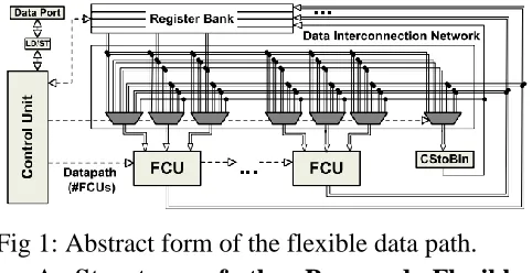
allocation and data communication patterns per kernel) can be mapped onto the proposed architecture using post-RTL data path interconnection sharing techniques [9], [7], [8]. The control unit drives the overall architecture (i.e., communication between the data port and the register bank, configuration words of the FCUs and selection signals for the multiplexers) in each clock cycle.
Fig 1: Abstract form of the flexible data path.
A. Structure of the Proposed Flexible
Computational Unit:
The structure of the FCU has been designed to enable high-performance flexible operation chaining based on a library of operation templates [4], [7]. Each FCU can be configured to any of the T1–T5 operation templates. The proposed FCU enables intra template operation chaining by fusing the additions performed before/after the multiplication and performs any partial operation template.
B. DFG Mapping Onto the Proposed
FCU-Based Architecture:
In order to efficiently map DSP kernels onto the proposed FCU-based accelerator, the semiautomatic synthesis methodology presented in [7] has been adapted. At first, a CS-aware transformation is performed onto the original DFG, merging nodes of multiple chained additions/subtractions to 4:2 compressors. A pattern generation on the transformed DFG
clusters the CS nodes with the multiplication operations to form FCU template operations. The designer selects the FCU operations covering the DFG for minimized latency.
Given that the number of FCUs is fixed, a resource-constrained scheduling is considered with the available FCUs and CStoBin modules determining the resource constraint set. The clustered DFG is scheduled, so that each FCU operation is assigned to a specific control step. A list-based scheduler [12] has been adopted considering the mobility2 of FCU operations. The FCU operations are scheduled according to descending mobility. The scheduled FCU operations are bound onto FCU instances and proper configuration bits are generated. After completing register allocation, a FSM is generated in order to implement the control unit of the overall architecture.
3.
Experimental Results
A. Circuit-Level Exploration of the
Proposed FCU With Respect to Technology Scaling:
multipliers of the FCC were imported from the Synopsys DesignWare library [11].
Fig 2:Area-time diagram of FCUs.
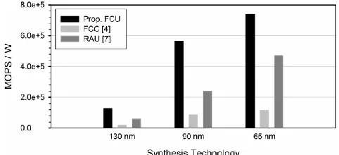
Fig. 2 reports the area complexity of the evaluated units at 130, 90, and 65 nm of synthesis technology. At 130 nm, the proposed FCU, the FCC, and the RAU operate without timing violations starting at 2.98, 4.83, and 1.99 ns, respectively. At 90 nm, the proposed FCU, the FCC, and the RAU are timing functional starting at 1.66, 2.46, and 1.01 ns, respectively. In addition, at 65 nm, the proposed FCU, the FCC, and the RAU start operating without timing violations at 1.13, 1.68, and 0.67 ns, respectively. Fig. 3 shows the MOPS/W values for the proposed FCU, the FCC, and the RAU at their critical clock periods with respect to the synthesis technology. For each unit, we consider the templates with the largest number of active operations without overlapping the one another and calculate the average ((#Ops)/(#Cycles)) factor. The #Ops derives from the two’s complement arithmetic operations (additive or multiplicative). For CS-aware units, i.e., FCU and RAU, the CStoBin module runs in parallel with the FCU or RAU, thus counting as one additive operation.
Fig 3: MOPS/W values of FCUs at the lowest achievable clock periods with respect to the synthesis technology.
4.
Conclusion
In this brief, we introduced a flexible accelerator architecture that exploits the incorporation of CS arithmetic optimizations to enable fast chaining of additive and multiplicative operations. The proposed flexible accelerator architecture is able to operate on both conventional two’s complement and CS-formatted data operands, thus enabling high degrees of computational density to be achieved. Theoretical and experimental analyses have shown that the proposed solution forms an efficient design tradeoff point delivering optimized latency/area and energy implementations.
6. References
[1] P. Ienne and R. Leupers, Customizable Embedded Processors: Design Technologies and Applications. San Francisco, CA, USA: Morgan Kaufmann, 2007.
[3] B. Mei, S. Vernalde, D. Verkest, H. D. Man, and R. Lauwereins, “ADRES: An architecture with tightly coupled VLIW processor and coarse-grained reconfigurable matrix,” in Proc. 13th Int. Conf. Field Program. Logic Appl., vol. 2778. 2003, pp. 61–70.
[4] M. D. Galanis, G. Theodoridis, S. Tragoudas, and C. E. Goutis, “A high-performance data path for synthesizing DSP kernels,” IEEE Trans. Comput.-Aided Design Integr. Circuits Syst., vol. 25, no. 6, pp. 1154–1162, Jun. 2006.
[5] K. Compton and S. Hauck, “Automatic design of reconfigurable domainspecific flexible cores,” IEEE Trans. Very Large Scale Integr. (VLSI) Syst., vol. 16, no. 5, pp. 493–503, May 2008.
[6] S. Xydis, G. Economakos, and K. Pekmestzi, “Designing coarse-grain reconfigurable architectures by inlining flexibility into custom arithmetic data-paths,” Integr., VLSI J., vol. 42, no. 4, pp. 486–503, Sep. 2009.
[7] S. Xydis, G. Economakos, D. Soudris, and K. Pekmestzi, “High performance and area efficient flexible DSP datapath synthesis,” IEEE Trans. Very Large Scale Integr. (VLSI) Syst., vol. 19, no. 3, pp. 429–442, Mar. 2011.
[8] G. Ansaloni, P. Bonzini, and L. Pozzi, “EGRA: A coarse grainedreconfigurable architectural template,” IEEE Trans. Very Large Scale Integr. (VLSI) Syst., vol. 19, no. 6, pp. 1062–1074, Jun. 2011.
[9] M. Stojilovic, D. Novo, L. Saranovac, P. Brisk, and P. Ienne, “Selective flexibility: Creating domain-specific reconfigurable arrays,” IEEE Trans. Comput.-Aided Design Integr. Circuits Syst., vol. 32, no. 5, pp. 681–694, May 2013.
[10] R. Kastner, A. Kaplan, S. O. Memik, and E. Bozorgzadeh, “Instruction generation for hybrid reconfigurable systems,” ACM Trans. Design Autom. Electron. Syst., vol. 7, no. 4, pp. 605– 627, Oct. 2002.
[11] [Online]. Available: http://www.synopsys.com, accessed 2013.
Authors Profile’s
Mrs.K.Radha has completed her AMIE in Electronics and Communication Engineering.She has master degree in Digital Electronics and Communication Systems,Gudlavalleru Engineering College,Gudlavalleru. She is pursuing Ph.D from JNTUK,Kakinada.Her main area of interest is VLSI Design.She is presently working as an Associate Professor in ECE Department, Medha Institute of Science and Technology for Women, Khammam.She is having 7 years of experience in teaching.
K.Anusha
M-Tech Medha Institute of Science and Technology for Women, Khammam
Dr. Murali Malijeddi