R E S E A R C H
Open Access
RF low power subsampling architecture for
wireless communication applications
Fanzhen Meng
1,2*, Hong Liu
1, Mingliang Wang
1, Xiaolin Zhang
1and Tong Tian
1,2Abstract
With the increasing demands of wireless communication, flexible, complex, and diversified wireless communication applications are required. However, the difficulty of enabling new wireless communication applications is the lack of low power radio frequency (RF) transmission devices, especially the RF receiver. In order to alleviate this problem, an RF low power subsampling architecture for wireless communication applications is proposed in this paper. This subsampling architecture adopts a single-ended to differential configured balun low noise amplifier (balun-LNA), a subsampling mixer with high sampling ratio and a finite input response (FIR) filter and infinite impulse response (IIR) filter achieving frequency down-conversion, avoiding using high power-hungry blocks. Based on a subsampling theory, an optimum sampling frequency for the subsampling architecture is necessary to relax the complexity of the system. For the application of internet of things (IoT) wireless communication, the paper provides the implementation of the subsampling receiver solutions to get a tradeoff between power consumption, gain, noise, and sensitivity. It can achieve −85 dBm sensitivity for an amplitude shift keying (ASK) modulation at the data rate of 1 Mbps with the clock sampling frequency of 40 MHz. Finally, the theoretical analysis and simulation results show that the performance of the subsampling architecture has several advantages over others.
Keywords:RF subsampling receiver, balun-LNA, 780 MHz IoT, Low power
1 Introduction
Thanks to the evolvement of the CMOS technology, the RF integrated circuits can improve integration and reduce chip area greatly. With the improving demands for wireless communication and the emerging new tech-nologies in recent few years, there is growing attention on sub 1 GHz Industrial, Scientific, and Medical (ISM) bands [1]. Different regulations are applied in different countries, for example, in the USA, the band from 902 to 928 MHz is adopted, with central frequency 915 MHz, while in Europe and China, the bands from 863 to 868 MHz and 755 to 787 MHz are applied, re-spectively [1, 2]. Most of these standards focus on high integration, low power, low cost, and multi-mode [3]. Especially, low power and high flexibility are of great im-portance [4, 5].
Although some low power architectures of receiver have been reported, such as direct conversion architecture and
low intermediate frequency (IF) architecture [6–8], highly power-hungry blocks such as LO and RF PLL are still existing in the circuits. Fortunately, the concept of new sampling technique is introduced in [9], called software-defined radio (SDR), which can directly digitize and de-modulate all signal from the antenna by A/D converter (ADC). Although this sampling technique can massively reduce power consumption of the system without using RF/analog blocks, it increases the memory of ADC which cannot be achieved by using the existing technologies. Moreover, a specific architecture of new RF sampling approaches can directly down-convert RF signals to base-band signals and achieve signal processing and demodula-tion in the digital circuits, which can minimize the number of RF and analog blocks [10–12]. For example, RF front-end mainly includes a low noise amplifier and a mixer, which achieves subsampling frequency conversion with clock down-sampling with embedded filtering [12]. However, the fixed filters restrict flexibility of the receiver, which cannot be suited for more channel transmission.
Meanwhile, regardless of RF PLL, subsampling receivers have great advantages in terms of power consumption and * Correspondence:[email protected]
1Shanghai Institute of Microsystem and Information Technology, Chinese
Academy of Sciences, Shanghai, China
2
University of Chinese Academy of Sciences, Beijing, China
flexibility by adopting low sampling frequency [13, 14]. For example, the multi-channel receiver with channel filtering at RF has been reported in [14], which can achieve −78 dBm sensitivity at 10−3 BER for BFSK modulation. However, the architecture based on the BAW resonator has been implemented, which cannot be integrated for the system. In order to improve in-tegration of the subsampling receiver, the number of extra exponents should be minimized. An active balun-LNA with the noise-cancelling technique in-stead of off-chip balun can be used [15–17]. For ex-ample, the active balun-LNA for GPS can exhibit a power consumption of 3.6 mW and a noise figure of 1.8 dB [17]. Moreover, low supply voltage can make power consumption further reduced [18, 19], with the 0.5 V supply voltage, the total power consumption of the receiver is about 1.15 mW [19]. However, low supply voltage can lead to the nonlinear effects and increase the noise figure of the system [20]. In addition, a quadrature down-conversion technique can greatly improve efficiency of signal frequency conversion, such as subsampling receiver with Q -en-hanced RF filtering exhibiting −87 dBm sensitivity at 10−3BER [21].
In this paper, design of the subsampling architecture should be tradeoff between integration, sensitivity, noise figure, and power consumption for the applica-tion of IoT. In order to solve the problem of noise folding, the subsampling receiver with integrated filter before the subsampling mixer can be used. In terms of sensitivity and integration of the system, the balun-LNA based on the inductively degenerated structure is used to achieve high voltage gain and low noise figure. And it adopts the gate and common-source cascade topology to provide differential output signal. Moreover, the sampling frequency with high sampling ratio can be used to further reduce the power consumption. And quadrature sampling tech-nique can acquire high energy efficiency. Therefore, the subsampling architecture with on-chip balun-LNA is proposed in this paper, which can achieve the quadrature sampling frequency conversion by low sampling frequency. This paper is organized as fol-lows: a brief overview of related works is described in Section 2. And the theory analysis of it is introduced in Section 3. The proposed RF subsampling receiver and its building blocks are introduced in Section 4. The performance of the subsampling receiver is ex-hibited in Section 5. Finally, conclusions and discus-sion are drawn in Section 6.
2 Related works
Traditionally, an RF subsampling architecture can use a subsampling mixer to achieve frequency conversion, like
a superheterodyne receiver. And it still adopts the synthesizer to provide sampling signal [13]. Moreover, a sampling clock jitter or high noise figure cannot be avoided, because of many folded noises emerging in the system. In addition, high sampling frequency with low sampling ratio used to down-convert RF signal to intermediate frequency or baseband, which can in-crease the complexity and power consumption of the system [22].
which generates many folding noises in subsampling architectures [34]. Thus, bandpass filter before a sub-sampling mixer should be used to reduce the noise folding. As an example, a 2.4-GHz RF sampling receiver was reported with an input sampling rate of 1072 MS/s [35], which can fulfill the signal demodulation. How-ever, the size and the power consumption of the system would be increased by high sampling frequency and complex down-conversion filter. And a high precision ADC is used to improve dynamic range of the system. Such as a continuous-time (CT) delta-sigma modulator (DSM) can demodulate signal for RF subsampling re-ceivers, which can achieve high dynamic range of the modulator for OSR = 64 at the cost of high complexity of the system [36]. In order to achieve multi-channels and multi-standard applications, a flexible subsampling frequency can be adopted to down-convert RF signal to intermediate frequency or baseband. For example, multi-standard RF subsampling receiver architecture is reported in [37], which includes two subsampling stages: first stage with the fixed subsampling frequency and second stage by a tunable IF sampling frequencies clock. It can achieve frequency conversion for a GSM, UMTS, and IEEE-802.11g multi-standard receiver. However, a tunable bandpass RF filter and an IF bandpass filter increase the complexity of the system. In order to further improve the sensitivity and reduce the power con-sumption of the receiver, high sampling ratio and highQ filter can be used in the subsampling receiver. For ex-ample, a subsampling receiver can achieve −91 dBm sensitivity at 10–3 BER for pi/4-DQPSK modulation with low power [38]. However, Q enhancement with the tuning LNA can increase the complexity of the system. Taking the above problems into consideration, the detail analysis for the RF subsampling architec-tures should be introduced.
3 RF subsampling architecture and theory 3.1 Subsampling theory
The simple diagram of RF subsampling receiver is shown in Fig. 1, which includes a LNA, a subsampling mixer, and baseband demodulation blocks. The RF signal com-ing from antenna is filtered and amplified by LNA, and
sampled and down-converted to baseband by the sub-sampling mixer, achieving subsub-sampling frequency con-version. Finally, the baseband (BB) can fulfill signal demodulation in the digital circuits.
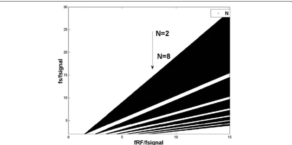
The frequency conversion of RF subsampling re-ceiver is shown in Fig. 2; RF signal is transferred to low intermediate frequency fIF by a proper local sam-pling frequency fs [13], and further converted to base-band. There are some folding images existing into a frequency down-conversion process, which seriously interferes with the information signal [14]. In order to avoid folded images, a high Qfilter should be used before a subsampling mixer. Moreover, it is very im-portant to choose a sampling frequency for achieving the frequency down-conversion. According to the Nyquist Theorem, the local sampling frequency must be more than twice of the bandwidth of the informa-tion signal. Meanwhile, in order to avoid aliasing noises, the local sampling frequency should meet the following Eqs. (1) and (2) as follows:
fs≥2fsignal ð1Þ
2fRFþfsignal
Nþ1 ≤fs≤
2fRF−fsignal
N N¼1;2;3;… ð2Þ
where Nis a subsampling ratio, fRFand fsare RF signal
frequency and a local sampling frequency, respectively,
fsignal is the bandwidth of information signal. From Eqs.
(1) and (2), the local sampling frequency fsis mainly de-termined by RF frequencyfRFand the sampling ratioN,
as shown in Fig.3. WhenfRFis constant, the larger
sam-pling ratioNis, the smaller the allowable local sampling frequency range is. However, a high sampling rate would increase the complexity of ADC. Thus, the local sam-pling frequency should be considered carefully. For the applications of IoT wireless communication, the sub-sampling receiver operates at the RF signal frequencyfRF
of 780 MHz with the bandwidth of 20 MHz. At the data rate of 1 Mbps, the local sampling frequency fs should be more than 2 MHz. Because of the allowable range of the local sampling frequency fs, the sampling ratio N cannot be more than 50.
In order to avoid DC drift and flicker noise of zero intermediate frequency architecture, the subsampling architecture samples and down-converts RF signal to low IF signal. Furthermore, it can be translated to quad-rature I/Q path signal by one clock signal. And then the local sampling frequency is defined as follows:
fs¼ 4fRF
2N−1; N¼1;2;3;… ð3Þ
The phase difference between adjacent samplesΔΦ is provided as follows:
ΔΦ¼2πffRF s ¼ 2
N−1
ð Þπ
2; N ¼1;2;3;… ð4Þ
From Eqs. (3) and (4), the intermediate frequency IF can be expressed as follows:
fIF¼jfRF−Hfsjmin¼fs=4 H¼1;2;3;… ð5Þ
When SIF is defined as the IF signal, the quadrature output at IF is provided as follows:
SI;M¼SIF;Mcos 2πfIF
M fs
¼SIF;M cos πM 2
SQ;M ¼SIF;M sin 2πfIF
M fs
¼SIF;Msin π
M
2
M¼1;2;3;… ð6Þ
where SI,M is I path IF signal, SQ,M is Q path IF signal. For example, based on the above equations from (3) to (6), the RF signal frequency fRF is 780 MHz with the
bandwidth of 20 MHz. When the sampling ratioNis 20, the local oscillation frequency is 80 MHz. The RF signal frequencyfRFcan be down-converted to the intermediate
frequencyfIF of 20 MHz. After a sample and hold (S/H)
mixer, the intermediate frequency fIF is classified into I
path SI,M and Q path SQ,M by the odd I path samples and the even Q path samples, respectively, which can further reduce the sampling rate and relax the com-plexity of ADC.
Fig. 2Frequency conversion of the subsampling receiver (RF signal is transferred to low intermediate frequency by using sampling frequency, and then further converted to baseband signal)
3.2 Voltage sampling and charge sampling
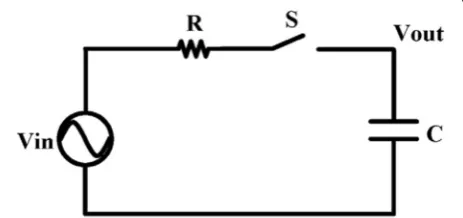
Generally, RF subsampling receivers mainly include voltage sampling and charge sampling architectures. Regarding system architecture, sampling principle and noise figure, two different architectures are analyzed to distinguish their respective advantages and disad-vantages. The diagram of the voltage sampling archi-tecture is shown in Fig. 4, including an ideal voltage source, a sampling switch S, a capacitor C, and a re-sistance R [13]. The sampling impulse clock can con-trol the switch, when the switch is ON, the sampling capacitor can sample and hold input signal voltage.
If input voltage signal isVin(t), output voltageVout(t) is given. Through Fourier transform, the frequency domain of the transfer functionH(f) is expressed as follows:
H fð Þ
j j ¼e−ffiffiffiffiffiffiffiffiffiffiffiffiffiffiffiffiffiffiffiffiffiffiffiffiðjatan 2ðτπfÞÞ 1þð2τπfÞ2
q ðτ¼RCÞ ð7Þ
From (7), the translated frequency has a maximum at DC and nulls at the n times of fs (n is integer), which can avoid the noise aliasing.
However, a diagram of charge sampling architecture is shown in Fig. 5, which includes an ideal voltage source, a transconductance stage Gm, a sampling switch Ss, a reset switch Sr and a capacitor C [27]. When the switch Ss is ON and Sr is OFF, the current translated by Gm is integrated into the capacitor C. And when switch Sr is ON and Ss is OFF, output sig-nal can be discharged and reset. Taking the Fourier transform, the transfer function H(f) of the charge sampling in frequency domain is defined as follows:
H fð Þ the integration window of the charge sampling architec-ture can be depended on sampling ratio f/fs. It has a maximum at DC and minimum at every multiplefs.
Based on the above different frequency response of volt-age sampling and charge sampling techniques, the −3 dB bandwidth of voltage sampling circuit is determined by the time constant τ, while charge sampling architecture just depends on integral window width.
3.3 Noise analysis
There are two main noises: thermal noise and flick noise in the subsampling architecture. With more harmonic mixing of subsampling frequency fs, noise folding would seriously affect noise figure of the system. In addition, the flick noise can be ignored in low-IF system.
In the voltage sampling architecture, thermal noise fromS/Hmixer is the main noise source. Comparatively speaking, others from ADC can be ignored. The equiva-lent noise ofS/Hmixer is expressed as follows:
V2n¼kT
C
1
N ð9Þ
where kT is thermal noise constant, N is the sampling ratio, andCis sampling capacitor.
In the charge sampling architecture, the thermal folded noise is also the main noise source. Since the bandwidth of the charge sampling architecture depends on the integral window width [26], noise power of ther-mal noise aliasing can be expressed as follows:
Pn¼Ti GCm
2
ð10Þ
Except for the thermal noise aliasing, the flick noise is other noise factor, which is provided by
V2n¼ K
CoxWL 1
f ð11Þ
where K/Cox could be regarded as the constant. There-fore, size ofW·L and capacitorCcan determine noises of the system.
According to the above analysis, the charge sampling architecture has more advantages in the high frequency and wideband receiver architecture. While the voltage Fig. 4The diagram of simple voltage sampling, including an ideal
voltage source, a sampling switchS, a capacitorC, and a resistanceR
Fig. 5The diagram of charge sampling, including an ideal voltage source, a transconductance stageGm, a sampling switchSs, a reset
sampling capacitor and resistor can be smaller enough to achieve better integration and higher gain. In order to simplify the structure and improve the flexibility of the system, the voltage sampling architecture is good suit-able for narrowband and low frequency fields, especially IoT application.
4 Subsampling architecture and circuits design 4.1 Subsampling architecture
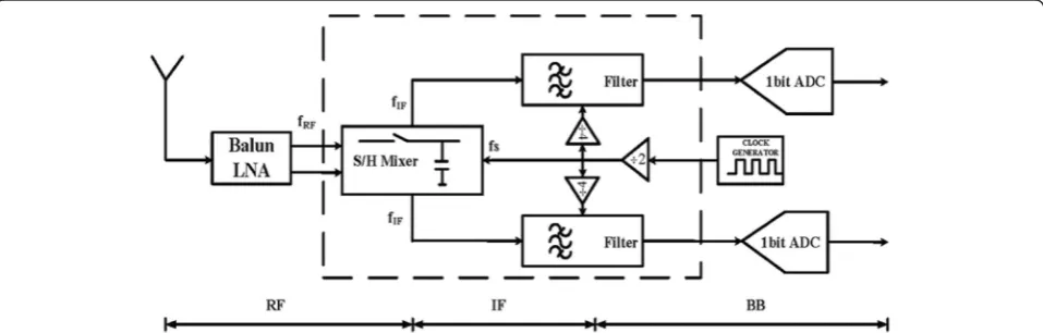
The traditional subsampling receiver mainly consists of a low noise amplifier (LNA), a sample and hold mixer, a complex bandpass filter, a clock generation, and an ADC. Usually, a single-ended input signal can be trans-ferred to differential signal by an off-chip balun, which increases the size of system. And the sample and hold mixer adopts simple MOS switches and sampling capac-itors to achieve frequency conversion, generating serious nonlinear effects and charge injection. Moreover, it adopts a high local sampling frequency to down-convert RF signal to IF signal. Therefore, the clock generation is needed to provide the high clock sampling frequency, which increases the power consumption of the subsamp-ling receiver. In addition, a clock generation based on high BAW resonators increases the size of the system.
For the requirements of wireless communication ap-plications of IoT, such as low data rate, low power consumption and high integration, a subsampling re-ceiver adopts a simple ASK modulation. In addition, a 1 bit ADC (such as comparator) can be used to de-modulate baseband signal. Compared to traditional subsampling receiver, the proposed subsampling re-ceiver architecture is shown in Fig. 6, which includes a balun low noise amplifier (balun-LNA), a two-stage passive sample and hold (S/H) mixer, an intermediate frequency amplifier (IFA), two down-conversion filters combined with a finite input response filter and an infinite impulse response filter, 1 bit ADCs and a
clock generator. The balun-LNA not only achieves a high gain and a low noise figure, but also provides the differential output signal, without using the off-chip balun. And the two-stage passive S/H mixer adopting complementary switches and capacitors can sample and translate RF signal to IF signal, which re-duces nonlinear effect and charge injection. In order to reduce folding noises, IF should be further filtered and decimated to baseband by down-conversion fil-ters, and baseband is demodulated and processed in digital circuits. A clock generator can provide local sampling signal, which can be translated to the clock sampling signal by two frequency dividers and the decimated sampling signal by D flip-flop. With the control of clock signal, RF signal is translated to IF by the S/H mixer and further decimated to baseband by the down-conversion filters.
According to the above subsampling theory analysis, the local oscillation frequency is 80 MHz with a sam-pling frequency of 40 MHz, and the decimated samsam-pling rate is 10 MHz. When RF input signal adopts ASK modulation at a data rate of 1 Mbps and ratio of mini-mum signal to noise SNRmin is about 13 dB, the total noise figure NF of the subsampling receiver could be ex-press as follows:
NF¼− −174dBmð þ10 logBWþSNRminÞ þPsens ð12Þ
where BW is the bandwidth of filter,Psensis the
sensitiv-ity of the subsampling receiver. From the expression (12), the total noise figure NF is determined by BW, SNRmin, andPsens. When the sensitivity of the
subsamp-ling receiver is −85 dBm with the 2-MHz bandwidth of filter, NF is 13 dB. Therefore, NF should be less than 9 dB, considering 3~4 dB loss. In order to meet the re-quirements of high sensitivity, low noise figure, and low power of the system, the total power consumption of the
subsampling receiver should be less than 4 mW and the total voltage gain of the system cannot be less than 60 dB when the subsampling receiver achieves−85 dBm sensitivity at 10−3BER. Further, with high noise figure of
S/Hmixer, the voltage gain of LNA should be more than 27 dB which reduces the total noise figure of the sub-sampling receiver.
4.2 Balun-LNA
In order to reduce the folding noise of the subsampling receiver, RF input signal should be filtered by the band-pass filter before S/H mixer. Although off-chip SAW/ BAW filter can achieve high Qto filter the interference and reduce the anti-aliasing noises, it is difficult to im-prove integration of the system. By using the frequency selective network and choosing the proper sampling fre-quency, the folded noises can be reduced.
With restraining a common-mode noise and reducing parasitic couplings, differential configuration is widely used in the LNA circuits. However, off-chip baluns used to achieve differential signal, which degrades integra-tion of the system. Tradiintegra-tionally, an active balun-LNA adopts the common-gate and common-source cascade topology to provide the differential signal output. How-ever, it is difficult to achieve a high voltage gain and generate the differential signal of phase opposite and equal amplitude under process variation. Therefore, the proposed balun-LNA adopting the noise-cancelling technique is shown in Fig. 7, which can acquire a differ-ential signal output. Firstly, transistor M1 achieves high
gain and better input impedance matching, with the in-ductors Ls, Lg, and capacitor Cg. And then transistors M2 and M3 are consisted of the common-gate common-source differential output topology, achieving noise cancelling and distortion cancelling. A single-end RF signal is transferred from the drain of M1 to the source of M2 and the gate of M3 through the capacitor
Cc, achieving differential output signal. Capacitor Cb provides AC coupling to ground and bias supply volt-age makes enough current, which avoids using the larger inductor L to balance the current of differential output topology. As the first block in the subsampling receiving chain, the performance of the balun-LNA is of great importance, which can determine the noise figure and the power consumption of the whole sys-tem. Considering requirements of wireless communi-cation for IoT applicommuni-cation, the voltage gain of the balun-LNA should be more than 25 dB, and the noise figure and the power consumption of the balun-LNA should be less than 2 dB and 2.5 mW, respectively. Moreover, the amplitude and the phase mismatch of the differential signal output remains, respectively, within 0.5 dB and 5°.
In order to analyze the noise figure of the balun-LNA in detail, the noise figure of every stage of LNA is listed, respectively [16]. Firstly, the noise figure NF1of M1 can be calculated as follows:
where the γ,δ,c are process parameters. NF1 is deter-mined by the transconductancegm1of M1 and the
gate-source capacitanceCgs1and capacitorCg.
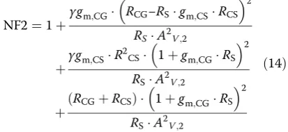
Secondly, the typical CG–CS topology is widely used in LNA, which has been analyzed in detail [15]. The noise figure NF2 of the CG–CS topology can be calcu-lated as follows:
Assuming that the transconductance gm,CS is n times bigger than the transconductance gm,CG and the load resistorRCGisntimes bigger than the load resistor RCS, which can achieve the equal voltage gain. When transis-tor M3 is matched,RSis the reciprocal of the transcon-ductance gm,CG (RS= 1/gm,CG). Therefore, the noise Fig. 7Balun-LNA, including common-source single-ended input and
figure NF2 and the voltage gain AV,2 of the CG–CS topology can be, respectively, rewritten as follows:
NF2¼1þ4γgm;CG
where NF2 is determined by the transconductancegm,CG
of M3 and the load resistor RCG. According to the
im-peding matching condition, the transconductance gm,CG
is 20 mS and theRSis 50Ω.γis about 4/3, and the load
resistor RCG is about 1000Ω so as to acquire high
voltage gain. Based on the simulation of Eqs. (15) and (16) by using the Matlab, NF2 of the CG–CS top-ology is clearly shown in Fig. 8. The noise figure NF2 becomes smaller by increasing the transconductance ratio n (n=gm,CS/gm,CG). For example, when the
transconductance ratio n is more than 4, NF2 of the system can be less than 1.5 dB. However, it is difficult to achieve transistors mismatching for higher n.
Considering impeding matching condition of CG tran-sistor M3, the noise figure cannot be further reduced. However, based on the inductively degenerated stage, the proposed balun-LNA achieves the lower noise figure for the large RSand small gm,CG. According to the cas-caded formula of noise figure, the total noise figure of the balun-LNA can be expressed as follows:
NF¼NF1þNF2−1
AV;1 ð
17Þ
Usually, the inductively degenerated cascade config-ured LNA has high voltage gain AV,1. Therefore, noise
figure NF1 has an important effect on the total noise figure NF of LNA.
4.3S/Hmixer
Generally, differential sample and hold (S/H) mixer cir-cuits include MOS switches and sampling capacitors. Without the high Q filter before S/H mixer, there are many folding noises affecting the information signal. In order to restrain the effect of folding noises, the pro-posed two-stage passive S/H mixer is shown in Fig. 9. Complementary switches constituted by NMOS and PMOS can reduce the charge injection. The differential output signal of the balun-LNA is sampled and con-verted to quadrature I path andQpath IF signals by the passive S/H mixer, respectively, without using high power-consuming RF PLL. However, after the first S/H mixer, RF interference signal still exists in the sampled signal. The second S/H mixer with the opposite clock sampling signal can be used to further fulfill the fre-quency conversion, which would relax the complexity of the following stages. Although the sampling capacitors should be large enough to reduce the kT/C noise, it would increase the size of theS/Hmixer. Therefore, the sampling capacitor should be tradeoff between noise and size of the system. For the application of IoT, the clock sampling frequency of 40 MHz can be used with the sampling ratio of 20, based on the analysis of the sam-pling frequency. And the total noise figure ofS/Hmixer and second-order filter can be obtained as follows:
NFmixer¼
whereQis the quality factor andRs is the resistor of an
ideal voltage source, and NF is determined by Csand fs. Based on the simulation of Eq. (18) by using the Matlab, the total noise figure NFmixer of S/H mixer is clearly
shown in Fig. 10. When Qis constant, noise figure be-comes smaller by increasing sampling local frequency fs
or sampling capacitor Cs. However, the high sampling
frequencyfsor large sampling capacitorCsincreases the
complexity of the system. Therefore, it is of great im-portance to choose the proper local sampling frequency for the subsampling receiver. For example, the sampling capacitorCsof 1 pF can be adopted for the system.
4.4 IFA and down-conversion filters
After frequency down-conversion of the S/H mixer, the weak IF signal should be amplified by the inter-mediate frequency amplifier (IFA). Traditionally, an operational amplifier (OPA) with resistance capaci-tance (RC) feedback used to amplify the IF signal, at the cost of increasing the size and the power con-sumption of the subsampling receiver. With two-stage Fig. 8Noise figure NF2 of the CG–CS topology for the transconductance
gm,CGis 20 mS,Rsis 50Ω,γis about 4/3, and the load resistorsRCGis
passive S/H mixer reducing folded noises, the sche-matic of the proposed single-stage IFA is shown in Fig. 11a, which is a simple two-stage amplifier. The input signal is amplified by the NMOS common-source amplifier with the current mirror load and the PMOS common-source amplifier with the resistive feedback [39]. IFA not only achieves the high voltage gain and reduces the power consumption but also ac-quires high isolation between the S/H mixer and the following stages. In addition, the resistive feedback configuration can improve the stability and provide enough phase margin which sacrifices a little noise figure of IFA.
In order to further reduce the folding noises emer-ging in the system, the typical complex down-conversion filters filter the frequency down-down-conversion signal. However, the lower the sampling frequency is, the smaller the orders of the down-conversion filters are. With the clock sampling frequency of 40 MHz for the subsampling receiver, the proposed discrete time
filtering combined with finite input response (FIR) filter and infinite impulse response (IIR) filter is shown in Fig. 11b. For example, four-tap FIR filter mainly in-cludes MOS switches and the sampling capacitors, which can achieve a high Qat the IF. Firstly, IF signal can be sampled and hold in capacitors C1~C4 for a period. And then the sampled signal can be charged into the total capacitorC5and integrated into capacitor
C6to output differentially, and the sizes of MOS tran-sistors and sampling capacitors are the same so as to avoid the mismatch. Furthermore, FIR filter can trans-fer IF signal to baseband by using the decimated clock sampling signal. With the four-tap samplers, FIR filter can also achieve the function of bandpass filter, which has nulls at all multiples of sampling frequency and maximum at all odd multiples of intermediate fre-quency. And the decimating sampling rate becomes a quarter sampling frequency, which can relax the re-quirements of ADC. In addition, the transfer function
H(z)of FIR filter is expressed as follows: Fig. 9Two-stage passiveS/Hmixer, consisting of complementary switches constituted by NMOS and PMOS and sampling capacitors
H zð Þ ¼1−z−1þz−2−z−3 z¼ejwTs ð19Þ
whereTsis the sampling cycle of four-tap FIR filter. The charge stored in the sampling capacitors can generate infinite impulse response (IIR), which has maximum at all multiples of sampling frequency and minimum at all odd multiples of intermediate frequency. Although the IIR filter reduces Q, it can still achieve maximum at all odd multiples of intermediate frequency.
4.5 Clock generator and 1 bit ADC
A clock generator usually adopts RF PLL to achieve the local sampling signal, which increases the complexity
and the power consumption of the system. Therefore, the proposed clock generator has high integration and low power consumption shown in Fig. 12, which mainly includes the amplifier stages, buffers, and D flip-flop. Firstly, differential input signal can be shaped and ampli-fied by the amplifier stages for LO signal. And then D flip-flops using the setting pulse excitation can generate the phased clock signal into clk1,clk1b,…,clk4b with the buffers. The waveforms of clock sampling generator can be shown in Fig. 13, andclk1~clk4and clk1b~clk4b can respectively decimate IF signal to quadratureI/Qoutput. To reduce the clock jitter, one clock is used to generate the clock sampling signal.
Finally, an ADC, the last block in the receiver, is used to demodulate signal. For the subsampling receiver of IoT application, 1 bit ADC such as comparator can be adopted to demodulate the simple ASK modulation signal. In addition, parallel NMOS and PMOS differential pairs of comparator are adopted to demodulate the baseband.
5 System performance
The proposed subsampling architecture for the RF re-ceiver is implemented, based on the transistor models of the United Microelectronics Corporation (UMC) 65 nm CMOS technology process by using the Cadence. In order to reduce the power consumption of the system, low threshold voltage NMOS and PMOS transistors were used
to simulate the performance of the system-level. Because of many sampling capacitors in the subsampling blocks, especially discrete time filtering combined with FIR filters and IIR filters, the smallest size of sampling capacitor was used to reduce the size of the system. Therefore, the core die area of the subsampling receiver is 1.1 mm*0.9 mm, including I/Opads with ESD protected. For the applica-tion of IoT wireless communicaapplica-tion, the proposed sub-sampling receiver operates at the RF signal frequency of 780 MHz with the bandwidth of 20 MHz and ASK signal at a data rate of 1 Mbps is used as the RF input modula-tion signal. The frequency down-conversion of the system can be achieved easily and flexibly by choosing the sam-pling frequency, based on input RF signal.
5.1 Current consumption
Based on the transistor models of CMOS process, the current consumption of the proposed subsampling cir-cuits is simulated by using the Cadence. With the volt-age supply of 1.2 V, the simulated results show that the total current consumption of the receiver is about 2.6 mA. And the current consumptions of the main blocks are listed in Table 1. Owing to lacks of high power-hungry blocks, such as RF PLL and high fre-quency LO, the proposed subsampling architecture achieves low current consumption. Moreover, the current consumption of the passiveS/Hmixer and FIR/ IIR can be neglected. In order to further analyze the Fig. 12A clock generator, mainly including the amplifier stages, buffers, and D flip-flop
Fig. 13Waveforms of clock generator and phased sampling clock, including the clock LO signal and decimated sampling signal
Table 1Current consumption of receiver
Blocks Current
LNA 1.6 mA
S/H 1μA
IFA 600μA
FIR/IIR 100 nA
1 bit ADC 300μA
current consumption of the main blocks, the current con-suming percentage of every block is shown in Fig. 14. And the current consumption of balun-LNA is 1.6 mA, which is 64 % of the total current consumption of the system. Moreover, IFA and 1 bit ADC current consumption con-sumes, respectively, 0.6 mA and 0.3 mA, which is about 24 and 12 %. However, in order to reduce the power con-sumption of the subsampling receiver immensely, the power consumption of the balun-LNA should be reduced by using new architecture or low threshold voltage tran-sistors, such as the supply voltage of 0.5 V.
5.2 S-parameters
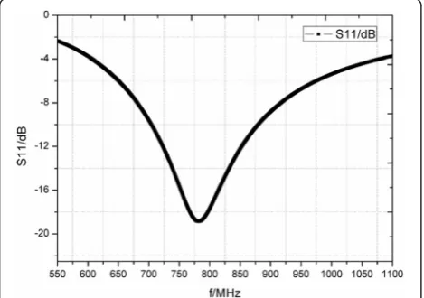
The performance of the subsampling receiver can be largely determined by the balun-LNA. By the inductively degenerated structure, the balun-LNA is used to achieve
high gain and low noise figure. Because of input imped-ing matchimped-ing usimped-ing larger inductor L, the impedance matching of the balun-LNA adopts the off-chip compo-nents. Based on the simulation of the LNA by using the Cadence, the results exhibit that S11 of LNA spacing from 550 MHz to 1.1 GHz is about −18 dB operating at 780 MHz as shown in Fig. 15. And the balun-LNA has a wider 3-dB bandwidth, which can meet the requirements of the signal transmission. In order to achieve differen-tial signal of the equal amplitude and phase opposite, the gain and phase balance of the CG–CS topology of the balun-LNA are considered with the noise and dis-tortion cancelling. Generally, the imbalance of the gain Fig. 14Current consumption percentage of the subsampling receiver (current consumption percentage of balun-LNA, IFA, and 1 bit comparator respectively are about 64, 24, and 12 %, and others can be neglected)
Fig. 15Input matching S11 of LNA spacing from 550 MHz to 1.1 GHz, and−18 dB operating at 780 MHz
and the phase of the balun-LNA are, respectively, within ± 0.5dB and ± 5o. According to the above ana-lysis, the ratio n between the transconductance gm,CS and the transconductancegm,CGis 4, which can achieve a low noise figure. Moreover, the balun-LNA has inte-grated the bandpass filter before the S/H mixer to re-duce the effect of folding noises.
5.3 System performance
According to analysis of the sampling frequency, the sampling ratioNbetween RF signal frequency and sam-pling frequency is very important to achieve frequency down-conversion. When input signal frequency is 780 MHz, a sampling ratio of 20 results in a sampling frequency of 40 MHz. RF signal frequency can be trans-ferred to intermediate frequency of 20 MHz by the sampling frequency. And the four-tap FIR filter is used
with the decimated sampling rate of 10 MHz, which has high Q at the intermediate frequency. Moreover, intermediate frequency is further down-converted to baseband by a decimated sampling rate. However, when input signal frequency is 780 MHz, a sampling ratio of 10 results in a sampling frequency of 80 MHz. RF signal frequency can be transferred to intermediate fre-quency (20 MHz) by sampling frefre-quency. However, eight-tap or more complex FIR filter should be used to achieve highQat the intermediate frequency, which in-creases the complexity of the down-conversion filter. In order to understand the frequency down-conversion of the subsampling receiver in detail, transient signal waveforms of the subsampling receiver is analyzed. If input signal frequency of 780.5 MHz is sampled by the clock sampling frequency of 40 MHz and input signal power level is −85 dBm, the output intermediate fre-quency is 500 KHz. The quadrature output waveforms of the subsampling receiver are shown in Fig. 16, based on the circuit simulation by using the Cadence. The time of transient waveforms is 10 ×e−6s. Further, the amplitude and phase mismatch of quadrature output signal remains respectively within 0.5 dB and 5°.
Considering the sensitivity of the subsampling archi-tecture, system simulation of a bit error rate (BER) can be analyzed based on different input power levels. The subsampling receiver for the application of IoT adopts the ASK modulation at a data rate of 1 Mbps. Firstly, a pseudo random code source regarded as transmitted data can be generated by the Matlab, and the subsamp-ling receiver can achieve frequency down-conversion and acquire demodulation signals with the Cadence simulation. And then different demodulated signals can be acquired according to different power levels of input signal. Compared to the transmitted data and demodu-lated data, the BER of the subsampling receiver is Fig. 17Bit error rate for a different input power for the ASK
modulation at a data rate of 1 Mbps (a range of input power level from−95 to−77 dBm)
analyzed and calculated by the Matlab. The sensitivity of the system is about −85 dBm for a BER of 10−3, which is shown in Fig. 17. If using a high Q filter re-duces the noise folding, the sensitivity of the system can be further improved.
In order to further exhibit the performance of the sub-sampling receiver, the waveforms of transmitted and re-ceived signal are exhibited in Fig. 18, and the time of the transient waveforms is 60 ×e−6s. When input signal power level is −85 dBm with input signal frequency of 780 MHz and the clock sampling frequency of 40 MHz, the maximum voltage gain of the whole system is 67 dB. In addition, noise figure of the system is about 6.5 dB by using the equation (12). The above waveform is the transmitted modulation signal with the data rate of 1 Mbps, and then the following waveform is baseband signal down-converted byS/Hmixer and filtered by the discrete time filtering combined FIR and IIR. The last waveform is the demodulation output signal. In addition, the information signal can be recovery from the demo-dulated signal by using the clock sampling signal.
The comparison of the proposed receiver with other receivers is listed in Table 2. The subsampling receiver has higher gain and lower noise figure, while still con-suming low power. Thanks to the balun-LNA with the noise-cancelling technique and four-tap FIR filter, the noise figure of the system is improved.
6 Conclusions
The proposed subsampling architecture for the RF re-ceiver achieves frequency down-conversion and signal demodulation for wireless communication applications. From the aspects of system architecture, sampling principle and noise figure, the proper clock sampling fre-quency of 40 MHz is used to transfer the RF signal to the quadratureIpath andQpath IF signals, respectively, at low power operation. Moreover, the balun-LNA and the passiveS/Hmixer without using RF PLL can guaran-tee high voltage gain and low noise figure of the sub-sampling architecture. Considering other performances,
such as power consumption, voltage gain, noise figure, and sensitivity, the proposed architecture is well suited for the narrowband wireless communication applica-tions. Further, low voltage supply and the advanced CMOS technologies reduce power consumption of the system significantly.
The noise figure of the system is further improved by using theQenhancement technique. Although the receiver has already exhibited good performance with the simple ASK modulation and the sampling ratio of 20, more ad-vanced modulation and the higher sampling ratio can be used to further improve the performance of the system.
Competing interests
The authors declare that they have no competing interests.
Received: 2 February 2016 Accepted: 24 April 2016
References
1. W Sun, M Choi, S Cho, IEEE 802.11ah: a long range 802.11 WLAN at sub 1 GHz. Journal of ICT Standardization, IEEE1((), 89–92 (2013)
2. Z Lin, P Mak, R Martins, A sub-GHz multi-ISM-band ZigBee receiver using function-reuse and gain-boosted N-path techniques for IoT applications. J. Solid-State Circuits, IEEE49(12), 2990–3004 (2014)
3. R Xu, C Nguyen, An ultra-wideband low power-consumption low noise-figure high-gain rf power-efficient DC–3.5-GHz CMOS integrated sampling mixer subsystem. Trans Microw Theory Tech56(5), 1069–1075 (2008) 4. F Meng, H Liu, T Tian,A 780-MHz low power transceiver for wireless nodes
applications in Internet of Things. Proceedings of IEEE 56th International Midwest Symposium on Circuits and Systems (MWSCAS): Aug 2013; Columbus, OH, United States,2013
5. M Kitsunezuka, K Kunihiro,A 5–9-mW 0.2–2.5-GHz CMOS low-IFreceiver for spectrum-sensing cognitive radio sensor networks. Proceedings of IEEE Radio Frequency Integrated Circuits Symposium (RFIC): June 2013; Seattle, WA, United States,2013
6. S Verma, J Xu, M Hamada, T Lee, A 17-mW 0.66-mm direct-conversion receiver for 1-Mb/s cable replacement. J. Solid-State Circuits, IEEE40(12), 2547–2554 (2005)
7. T Nguyen, V Krizhanovskii, J Lee, S Han, S Lee, N Kim, C Pyo, A low-power RF direct-conversion receiver/transmitter for 2.4-GHz-band IEEE 802.15. 4 standard in 0.18-CMOS technology. Trans Microw Theory Tech IEEE54(12), 4062–4071 (2006) 8. I Nam, K Choi, J Lee, H Cha, B Seo, K Kwon, K Lee, A 2.4-GHz low-power low-if
receiver and direct-conversion transmitter in 0.18-CMOS for IEEE 802.15. 4 WPAN applications. Trans Microw Theory Tech IEEE55(4), 682–689 (2007) 9. J Mitola, The software radio architecture. IEEE Commun. Mag.33(5), 26–38 (1995) 10. A Karim, L Kokarovtseva, J Velazquez, R Genov, 915-MHz FSK/OOK wireless
neural recording SoC with 64 mixed-signal FIR filters. J. Solid-State Circuits, IEEE48(10), 2478–2493 (2013)
Table 2Performance comparison
Reference MWSCAS 13 [4] JSSC 13 [10] JSSC 13 [14] ISSCC 14 [18] JSSC 12 [21] This work
Rx architecture Direct IF SDR Subsampling Low IF Subsampling Subsampling
Technology (CMOS) 65 nm 0.13μm 0.18μm 65 nm 0.18μm 65 nm
Data rate 1 Mbps 1.5 Mbps 268 kbps – – 1 Mbps
Input frequency 780 MHz 915 MHz 2.433 GHz 860 MHz 2.4 GHz 780 MHz
11. J Mitola, Software radio architecture: a mathematical perspective. J Selected Areas Commun IEEE17(4), 514–538 (1999)
12. A Abidi, The path to the software-defined radio receiver. J. Solid-State Circuits IEEE42(5), 954–966 (2007)
13. C DeVries, D Ralph, Subsampling architecture for low power receivers. Trans Circuits Syst II: Express Briefs IEEE55(4), 304–308 (2008)
14. A Heragu, D Ruffieux, C Enz, A 2.4-GHz MEMS-based PLL free multi-channel receiver with multi-channel filtering at RF. J. Solid-State Circuits IEEE
48(7), 1689–1700 (2013)
15. S Blaakmeer, E Klumperink, D Leenaerts, B Nauta, Wideband balun-lna with simultaneous output balancing, noise-canceling and distortion-canceling. J. Solid-State Circuits IEEE43(6), 1341–1350 (2008)
16. F Chen, W Zhang, W Rhee, J Kim, D Kim, Z Wang, A 3.8-mW 3.5–4GHz regenerative FM-UWB receiver with enhanced linearity by utilizing a wideband LNA and dual bandpass filters. Trans Microw Theory Tech IEEE
61(9), 3350–3359 (2013)
17. Y Ji, C Wang, J Liu, H Liao, 1.8 dB NF 3.6 mW CMOS active balun low noise amplifier for GPS. Electron Lett 4th IEEE46(3), 251–252 (2010)
18. C Salazar, A Kaiser, A Cathelin, J Rabaey,A -97dBm-Sensitivity Interferer-Resilient 2.4GHz Wake-Up Receiver Using Dual-IF Multi-N-Path Architecture in 65 nm CMOS. in IEEE Int. Solid-State Circuits Conf.(ISSCC): Feb 2015; San Francisco, CA, United States,2015
19. Z Lin, P Mak, R Martins,A 0.5 V 1.15 mW 0.2 mm2 Sub-GHz ZigBee Receiver Supporting 433/860/915/960 MHz ISM Bands with Zero External Components. in IEEE Int. Solid-State Circuits Conf.(ISSCC): Feb 2014; San Francisco, CA, United States,2014
20. R Vaughan, N Scott, D White, The theory of bandpass sampling. Trans. Signal Process, IEEE39(9), 1973–1984 (1991)
21. R Mason, J Fortier, C DeVries Complete, SOC transceiver in 0.18 um CMOS using Q-enhanced filtering, sub-sampling and injection locking. J. Solid-State Circuits, IEEE47(8), 1800–1809 (2012)
22. H David, C Hwang, B Lusignan, W Bruce, A 900-MHz RF front-end with integrated discrete-time filtering. J. Solid-State Circuits, IEEE31(12), 1945–1954 (1996) 23. S Chen, B Robert, A Subsampling, Radio architecture for ultrawideband
communications. Trans Signal Process IEEE55(10), 5018–5031 (2007) 24. M Huang, T Chiu, A Quadrature, Charge-domain filter with frequency
downconversion for RF receivers. Trans Microw Theory Tech IEEE58(5), 1323–1332 (2010)
25. G Xu,Y Jiren,Comparison of charge sampling and voltage sampling. Proceedings of 43rd IEEE Midwest Symposium on Circuits and Systems: Aug 2000; Lansing, MI, United States,2000
26. S Karvonen, T Riley, J Kostamovaara, Charge-domain FIR sampler with programmable filtering coefficients. Trans Circuits Syst II: Express Briefs IEEE
53(3), 192–196 (2006)
27. G Baptiste, A Frappe, A Kaiser, A Reconfigurable, IF to DC sub-sampling receiver architecture with embedded channel filtering for 60 GHz applications. Trans Circuits Syst I: Regular Papers, IEEE60(5), 1220–1231 (2013)
28. Y Zhou, Y Fei, Cascaded charge-domain sampling mixer with embedded sinc3FIR and four-path filters for software-defined radio. Electron Lett IEEE 50(3), 216–218 (2014)
29. Z. Xu, et al.Crowdsourcing based Description of Urban Emergency Events using Social Media Big Data. IEEE Transactions on Cloud Computing,10.1109/ TCC.2016.2517638 (2016)
30. Z. Xu, et al. Crowdsourcing based Social Media Data Analysis of Urban Emergency Events.Multimedia Tools and Applications, 10.1007/s11042-015-2731-1 (2015) 31. Z Xu et al., Participatory Sensing based Semantic and Spatial Analysis of
Urban Emergency Events using Mobile Social Media. EURASIP J. Wireless Commun. Networking,44(1), 1-9 (2016)
32. B Carsten, L Ivan, I Umran,A 9 mW Direct RF Sampling GPS Receiver Front-End in 0.13μm BiCMOS. Proceedings of IEEE International Symposium on Circuits and Systems (ISCAS): May 2012; Seoul, Korea (South),2012 33. P Holly, H James, A 2.4 GHz CMOS sub-sampling mixer with integrated
filtering. J. Solid-State Circuits IEEE40(11), 2159–2166 (2005)
34. H Kim, J Kim, J Kim, H Wang, I Lee, The design method and performance analysis of RF subsampling frontend for SDR/CR receivers. Trans Ind Electron IEEE57(5), 1518–1525 (2010)
35. J Darius, F Kalle, D Jerzy, E Patrik, S Christer, A 2.4-GHz RF sampling receiver front-end in 0.18-um CMOS. IEEE J. Solid-State Circuits40(6), 2165–2177 (2005) 36. U Alper, C Ediz, K Izzet, A Continuous-Time, Delta-sigma modulator for
RF subsampling receivers. Trans Circuits Syst II: Express Briefs IEEE59(5), 272–276 (2012)
37. R Barrak, A Ghazel, F Ghannouchi, Optimized multistandard RF subsampling receiver architecture. Trans Wireless Commun IEEE8(6), 2901–2909 (2009) 38. J Cheng, N Qi, P Chiang, A Natarajan, A low-power, low-voltage
WBAN-compatible sub-sampling PSK receiver in 65 nm CMOS. J. Solid-State Circuits IEEE49(12), 3018–3030 (2014)
39. M Soer, E Klumperink, Z Ru, F Vliet, B Nauta,A 0.2-to-2.0GHz 65nm CMOS receiver without LNA achieving >11dBm IIP3 and <6.5 dB NF. in IEEE Int. Solid-State Circuits Conf.(ISSCC): Feb 2009; San Francisco, CA, United Solid-States,2009
Submit your manuscript to a
journal and benefi t from:
7Convenient online submission
7Rigorous peer review
7Immediate publication on acceptance
7Open access: articles freely available online
7High visibility within the fi eld
7Retaining the copyright to your article