ISSN (Online): 2278 – 8875
I
nternational
J
ournal of
A
dvanced
R
esearch in
E
lectrical,
E
lectronics and
I
nstrumentation
E
ngineering
(An ISO 3297: 2007 Certified Organization)
Vol. 4, Issue 5, May 2015
Comparative Study of SPWM & SVPWM Based
Three Phase Voltage Source Inverter for an Ups
System Operating Under Non Linear Loads
M A Wajid Mudassir1, Mohammed Ismail.B2, Dr. Mohammad Haseeb Khan3, Dr. Arshia Azam4
PG Student [PES], Dept of EEE, Muffakham Jah College of Engineering & Technology, Hyderabad, India1. Sr Asst. Professor, Dept of EEE, Muffakham Jah College of Engineering & Technology, Hyderabad, India2.
Professor, Dept of EEE, Muffakham Jah College of Engineering & Technology, Hyderabad, India3. Associate Professor, Dept of ECE, Polytechnic, Maulana Azad National Urdu University, Hyderabad, India4.
ABSTRACT: This research paper present the design, comparison of two different PWM techniques i.e. The sinusoidal PWM (SPWM) technique, and the space vector PWM (SVPWM) technique for three phase uninterruptible power supply (UPS) systems that are operating under nonlinear loads. First a model for Sinusoidal PWM is made and simulated using Matlab/Simulink software and its performance is compared with Space vector PWM. Matlab/Simulink is used to analyse, design & develop, the controller of the inverter. The controller is designed & compared by discussing their ease of implementation and by analysing the output harmonic spectra of various output voltages poles voltages, line to neutral voltages, and line to line voltages Power factor (PF) & their Total harmonic distortion (THD). Designing of the controller adds inner loops to the closed loop control system effectively that enables successful reduction of harmonics and compensation of distortion at the outputs. The performance is simulated using a three phase 10 kVA UPS Systems under all types of load conditions.
KEYWORDS: Space Vector Pulse Width Modulation (SVPWM), Sinusoidal Pulse Width Modulation (SPWM), Uninterruptible Power Supply (UPS), Voltage Source Inverter (VSI), Total Harmonic Distortion (THD).
I. INTRODUCTION
The increased use of rectifiers in critical loads employed by the information technologies, medical and militaryequipment mandate the design of uninterruptible power supplies (UPS) with high quality outputs. The highly nonlinear currents drawn especially by high power single phase rectifier loads greatly distort the UPS outputs. The distorted UPS voltages cause generation of low dc voltage at the output of the rectifier loads, which causes high current flow, increased power losses, and possibly the malfunction of the critical load or the UPS. In a UPS system, the inverter is responsible for synthesizing sinusoidal voltages from a dc source through the pulse width modulation (PWM) of the dc voltage. The inductive element here is needed to remove the switching frequency harmonics from the current waveform that are generated by the PWM operation of the inverter. The inductance value can be reduced if the switching frequency is increased. But, in practice, it has an upper limit at high power inverters due to the efficiency concerns and the switching device limitations. So, for the selected switching frequency and the power level, an optimum filter with a smallest inductance can be designed, but the distortion cannot be completely avoided, and the regulations and the customer specifications may not be satisfied.[1]
The solution to this problem is to design a proper inverter controller such that it generates a control signal with multiple functionalities. This signal must carry information to produce sinusoidal voltages with small steady state RMS error, to provide fast transient response and corrective actions to reduce distortion even under highly nonlinear loads. Therefore, a major research has been conducted to design such controllers for the high performance UPS systems. The high performance controllers in general employed multi loop state feedback control strategies to achieve the regulation specifications.
ISSN (Online): 2278 – 8875
I
nternational
J
ournal of
A
dvanced
R
esearch in
E
lectrical,
E
lectronics and
I
nstrumentation
E
ngineering
(An ISO 3297: 2007 Certified Organization)
Vol. 4, Issue 5, May 2015
method is still preferred by many manufacturers because of its implementation simplicity, easy tuning even under load, flexibility, and most importantly the advantages of controlling each phase independently.[1]
II. SYSTEM MODEL AND ASSUMPTIONS
The Block diagram of a typical three phase four wire transformer isolated UPS system is given in Fig. 1. The three phase thyristor based controlled rectifier converts the mains voltages into a constant dc and also provides standalone charge to the batteries. Then, a six switch PWM voltage source inverter (VSI) creates balanced three phase sinusoidal voltages across the load terminals at the utilization frequency and magnitude. The LC low pass filter removes the harmonics generated by the PWM switching. The winding of the transformer blocks the third harmonic currents at the inverter side, and the zigzag winding provides a neutral point and zero phase difference for the load side voltages. The load can be a three phase or a single phase load ranging from linear to nonlinear load with a crest factor up to 3. The UPS uses a digital controller implemented in a fixed point DSP controller.[3]
Fig. 1. Block diagram of a typical three phase four wire transformer isolated UPS system.
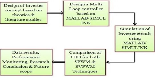
III. METHODOLOGY
The below Figure.2 indicates the methodology process used in this research which consist of five main stages. One after the other each stage is accomplished in a neat & simple manner
Fig. 2. The Research Methodology
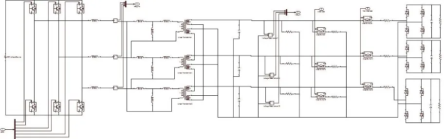
IV. DESIGN OF THE INVERTER POWER STAGE
ISSN (Online): 2278 – 8875
I
nternational
J
ournal of
A
dvanced
R
esearch in
E
lectrical,
E
lectronics and
I
nstrumentation
E
ngineering
(An ISO 3297: 2007 Certified Organization)
Vol. 4, Issue 5, May 2015
the element values of the LC filter. For that reason, selecting the nominal modulation ratio around 0.7 is considered optimum since it guarantees the linear PWM operation under the worst case.
The simulation studies have shown that if the controller goes into over modulation region, the THD specification cannot be satisfied. Therefore, the nominal dc bus voltage is maintained at 405 V when grid is okay and it
is allowed to reduce down to 300 V when grid is gone and the UPS operates from the battery pack. One string of the battery pack consists of 30 pieces of 12V lead acid batteries connected in series. The switching frequency is selected as 10.05 KHz. and based on our simulation studies, it has been realized that the output impedance of an inverter plays an important role in reducing the THD of the output voltage. Finally, the schematic of the inverter with the parameter values optimized for all load conditions is shown in Fig. 3.
Fig. 3. Simulink model of the designed inverter power stage including delta zigzag transformer, the LC filter, the measurements, and the linear and nonlinear loads.
V. SINUSOIDAL PULSE WIDTH MODULATION
The sinusoidal pulse width modulation (SPWM) technique produces a sinusoidal waveform by filtering an output pulse waveform with varying width. The desired output voltage is achieved by varying the frequency and amplitude of a reference or modulating voltage. The variations in the amplitude and frequency of the reference voltage change the pulse-width patterns of the output voltage but keep the sinusoidal modulation. The switches are controlled in pairs (S1,S4), (S3,S6), and (S5,S2) and the logic for the switch control signals is:[4]
S1 is ON when Va>VT S4 is ON when Va<VT
S3 is ON when Vb>VT S6 is ON when Vb<VT
S5 is ON when Vc>VT S2 is ON when Vc<VT
VI. SPACE VECTOR PULSE WIDTH MODULATION
Space Vector Modulation (SVM) was originally developed as vector approach to Pulse Width Modulation (PWM) for three phase inverters. It is a more sophisticated technique for generating sine wave that provides a higher voltage to the motor with lower total harmonic distortion. The main aim of any modulation technique is to obtain variable output having a maximum fundamental component with minimum harmonics. The six switching power devices can be constructed using power BJTs, GTOs, IGBTs etc. The choice of switching devices is based on the desired operating power level, required switching frequency, and acceptable inverter power losses. Two switches on the same leg cannot be closed or opened at the same time. SVPWM is a different approach from PWM modulation, based on space vector representation of the voltages in the α-β plane. The α-β components are found by Clark’s transformation. Space Vector PWM (SVPWM) refers to a special switching sequence of the upper three power transistors of a three phase power inverter.[4]
6.1 Principle of Space Vector PWM
ISSN (Online): 2278 – 8875
I
nternational
J
ournal of
A
dvanced
R
esearch in
E
lectrical,
E
lectronics and
I
nstrumentation
E
ngineering
(An ISO 3297: 2007 Certified Organization)
Vol. 4, Issue 5, May 2015
synchronously rotating frame (or) stationary frame. From these two phase components, the reference vector magnitude can be found and used for modulating the inverter output. The process of obtaining the rotating space vector is explained in the following section, considering the stationary reference frame. Considering the stationary reference frame let the three phase sinusoidal voltage component be,
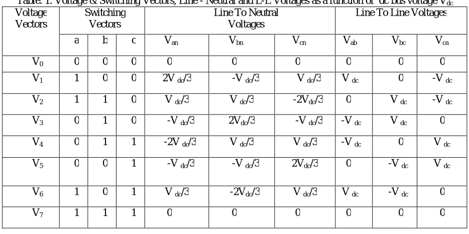
Va = Vm sin (ωt) (1) Vb = Vmsin (ωt - 2 π /3) (2) Vc = Vmsin (ωt - 4π/3). (3)
Fig. 4. Basic switching, vectors and sectors.
Table. 1. Voltage & Switching Vectors, Line - Neutral and L-L Voltages as a function of dc bus voltage Vdc
Voltage Vectors
Switching Vectors
Line To Neutral Voltages
Line To Line Voltages
a b c Van Vbn Vcn Vab Vbc Vca
V0 0 0 0 0 0 0 0 0 0
V1 1 0 0 2V dc/3 -V dc/3 V dc/3 V dc 0 -V dc
V2 1 1 0 V dc/3 V dc/3 -2Vdc/3 0 V dc -V dc
V3 0 1 0 -V dc/3 2Vdc/3 -V dc/3 -V dc V dc 0
V4 0 1 1 -2V dc/3 V dc/3 V dc/3 -V dc 0 V dc
V5 0 0 1 -V dc/3 -V dc/3 2Vdc/3 0 -V dc V dc
V6 1 0 1 V dc/3 -2Vdc/3 V dc/3 V dc -V dc 0
V7 1 1 1 0 0 0 0 0 0
The switches being ON or OFF, meaning 1 or 0 are determined by the location of the reference vector on this d-q plane. The switches 1, 3, 5 are the upper switches, and if these are 1 (separately or together) it turns the upper inverter leg ON and the terminal voltage (Va, Vb, Vc) is positive (+Vdc). If the upper switches are zero, then the
terminal voltage is zero. The lower switches are complementary to the upper switches, so the only possible combinations are the switching states: 000, 001, 010, 011, 100, 110, 110, 111. This means that there are 8 possible switching states, for which two of them are zero switching states and six of them are active switching states. Six non zero vectors (V1-V6) shape the axes of a hexagonal as depicted in Figure 4, and supplies power to the load. The angle
between any adjacent two non zero vectors is 600 degrees. Meanwhile, two zero vectors (V0 and V7) and are at the
origin and apply zero voltage to the load. The eight vectors are called the basic space vectors and are denoted by (V0, V1, V2, V3, V4, V5, V6, V7). The same transformation can be applied to the desired output voltage to get the desired
reference voltage vector, Vref in the d-q plane. The objective of SVPWM technique is to approximate the reference
ISSN (Online): 2278 – 8875
I
nternational
J
ournal of
A
dvanced
R
esearch in
E
lectrical,
E
lectronics and
I
nstrumentation
E
ngineering
(An ISO 3297: 2007 Certified Organization)
Vol. 4, Issue 5, May 2015
given by below equation.[5]
= Vdc
1 −1 0 0 1 −1
−1 0 1
(4)
= Vdc
1 −1 0 0 1 −1
−1 0 1
(5)
Where Vdc is the supply voltage or bus voltage. the eight combinations & the derived output line to line &
phase voltage in terms of dc supply voltage Vdc according to equations as shown in Table 1.
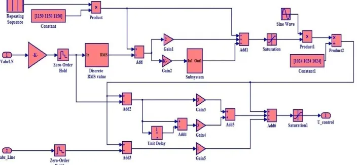
VII. CONTROLLER DESIGN
This section presents the design of the proposed inverter controller. The controller is based on the multi loop SPWM method as shown in Fig.5. The controller topology is very similar to the classical state feedback multi loop controllers, except that all the loops are combined instead of cascade connection before they are applied to the PWM generator. This feature basically adds the relative benefits of each loop and creates a more effective multi loop strategy. In order to facilitate the understanding of the proposed controller, the reasoning behind the selected control topology can be explained as follows. The control system shown in Fig.5 consists of one outer voltage loop and three inner loops. The outer loop is the main voltage loop, which regulates the fundamental frequency component of the output voltage and its steady state RMS value using a PI compensator.[1]
Fig. 5. Simulink model of the proposed Multi loop controller.
VII. EXPERIMENTAL RESULTS
ISSN (Online): 2278 – 8875
I
nternational
J
ournal of
A
dvanced
R
esearch in
E
lectrical,
E
lectronics and
I
nstrumentation
E
ngineering
(An ISO 3297: 2007 Certified Organization)
Vol. 4, Issue 5, May 2015
Fig. 6. Simulink model of the SPWM inverter system.
Fig. 7. Simulink model of the SVPWM inverter system.
Fig. 8. Inverter output Line-Line Current Ia, Ib, Ic
0 0.02 0.04 0.06 0.08 0.1 0.12 0.14 0.16 0.18 0.2
-50 0 50
Ia
0 0.02 0.04 0.06 0.08 0.1 0.12 0.14 0.16 0.18 0.2
-50 0 50
Ib
0 0.02 0.04 0.06 0.08 0.1 0.12 0.14 0.16 0.18 0.2
-50 0 50
Time
ISSN (Online): 2278 – 8875
I
nternational
J
ournal of
A
dvanced
R
esearch in
E
lectrical,
E
lectronics and
I
nstrumentation
E
ngineering
(An ISO 3297: 2007 Certified Organization)
Vol. 4, Issue 5, May 2015
Fig. 9. Three Phase inverter output Current Ia, Ib, Ic
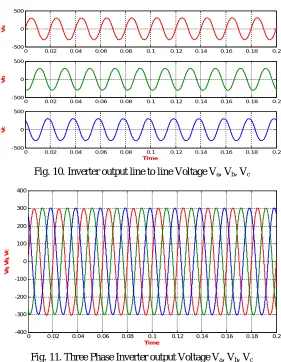
In fig 10,11. Inverter output Current are shown for both three phase system & single phase system of the voltage source inverter of the UPS system for both SPWM & SVPWM modulation techniques under all types of load
conditions.
Fig. 10. Inverter output line to line Voltage Va, Vb, Vc
Fig. 11. Three Phase Inverter output Voltage Va, Vb, Vc
0 0.02 0.04 0.06 0.08 0.1 0.12 0.14 0.16 0.18 0.2
-25 -20 -15 -10 -5 0 5 10 15 20 25
Time
I
a
,
Ib
,
Ic
0 0.02 0.04 0.06 0.08 0.1 0.12 0.14 0.16 0.18 0.2
-500 0 500
V
a
0 0.02 0.04 0.06 0.08 0.1 0.12 0.14 0.16 0.18 0.2
-500 0 500
V
b
0 0.02 0.04 0.06 0.08 0.1 0.12 0.14 0.16 0.18 0.2
-500 0 500
Time
V
c
0 0.02 0.04 0.06 0.08 0.1 0.12 0.14 0.16 0.18 0.2
-400 -300 -200 -100 0 100 200 300 400
Time
V
a
,
V
b
,
V
ISSN (Online): 2278 – 8875
I
nternational
J
ournal of
A
dvanced
R
esearch in
E
lectrical,
E
lectronics and
I
nstrumentation
E
ngineering
(An ISO 3297: 2007 Certified Organization)
Vol. 4, Issue 5, May 2015
In Fig 10,11. Inverter output voltages are shown for both three phase system & single phase system of the voltage source inverter of the UPS system for both SPWM & SVPWM modulation techniques under all types of load conditions.
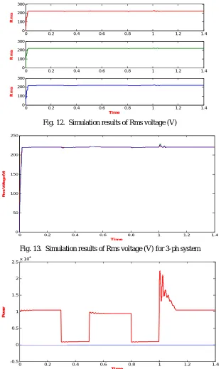
Fig. 12. Simulation results of Rms voltage (V)
Fig. 13. Simulation results of Rms voltage (V) for 3-ph system
Fig. 14. Three Phase Instantaneous Active & Reactive Power Wave Form for SPWM
0 0.2 0.4 0.6 0.8 1 1.2 1.4
0 100 200 300
R
m
s
0 0.2 0.4 0.6 0.8 1 1.2 1.4
0 100 200 300
R
m
s
0 0.2 0.4 0.6 0.8 1 1.2 1.4
0 100 200 300
Time
R
m
s
0 0.2 0.4 0.6 0.8 1 1.2 1.4
0 50 100 150 200 250
Time
R
m
s
V
o
lt
a
g
e
(
V
)
0 0.2 0.4 0.6 0.8 1 1.2 1.4
-0.5 0 0.5 1 1.5 2 2.5x 10
4
Time
P
o
w
e
ISSN (Online): 2278 – 8875
I
nternational
J
ournal of
A
dvanced
R
esearch in
E
lectrical,
E
lectronics and
I
nstrumentation
E
ngineering
(An ISO 3297: 2007 Certified Organization)
Vol. 4, Issue 5, May 2015
Fig. 15. Three Phase Instantaneous Active & Reactive Power Wave Form for SVPWM
In Fig 14,15. Three Phase Instantaneous Active & Reactive Power are shown for three phase system of the voltage source inverter of the UPS system for both SPWM & SVPWM modulation techniques under all types of load condition
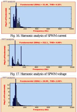
Fig. 16. Harmonic analysis of SPWM current
Fig. 17. Harmonic analysis of SPWM voltage
Fig. 18. Harmonic analysis of SVPWM current
0 0.2 0.4 0.6 0.8 1 1.2 1.4
-5000 0 5000 10000 15000 20000 Time P o w e r
0 200 400 600 800 1000
0 2 4 6 8 Frequency (Hz)
Fundamenta l (50Hz) = 31.48 , THD= 4.32%
M a g ( % o f F u n d a m e n ta l) Time (s)
0 200 400 600 800 1000
0 1 2 3 4
Fre que ncy (Hz)
Funda me ntal (50Hz) = 312.1 , THD= 4.00%
M a g ( % o f F u n d a m e n ta l) Time (s)
0 200 400 600 800 1000
0 2 4 6 8 10 12
Freque ncy (Hz)
Funda me ntal (50Hz) = 26.99 , THD= 2.04%
ISSN (Online): 2278 – 8875
I
nternational
J
ournal of
A
dvanced
R
esearch in
E
lectrical,
E
lectronics and
I
nstrumentation
E
ngineering
(An ISO 3297: 2007 Certified Organization)
Vol. 4, Issue 5, May 2015
Fig. 19. Harmonic analysis of SVPWM voltage
Table. 2. Comparison of Current & Voltage %THD for both SPWM & SVPWM Techniques
PWM technique % Current THD % Voltage THD
SPWM 4.32% 4.00%
SVPWM 2.04% 3.40%
IX. CONCLUSION
In this paper, SPWM and SVPWM techniques have been investigated and compared, for three phase UPS systems powering nonlinear loads. The load consists of three single phase rectifiers connected between each line and the neutral and absorbing power equal to the rated power of the UPS with a crest factor up to 3. During the investigations, we realized Total harmonic distortion, & Power factor in both techniques. The SPWM & SVPWM technique is applied to a three phase inverter and it is observed that SPWM increases the overall system efficiency.
The controller performance is evaluated experimentally using a three phase 10 kVA transformer isolated UPS. A THD equal to 4.00% & 4.32% at output voltage & current for SPWM is achieved & a THD equal to 3.40% & 2.04% at output voltage & current for SVPWM is achieved. It has been observed that SVPWM has showed superior performances due to less THD, greater PF and less switching losses because SVPWM utilizes advance computational switching technique to reduce THD. Furthermore, at high switching frequencies SVPWM gives better results as compared to SPWM. Thus, based on all obtained results, we concluded that SVPWM technique provides greater overall performance and efficiency as compared to SPWM technique.
REFERENCES
[1] Bunyamin Tamyurek, Member, IEEE, "A High Performance SPWM Controller for Three Phase UPS Systems Operating Under Highly Nonlinear Loads", IEEE Transactions On Power Electronics, Vol. 28, No. 8, August 2013.
[2] Phuong Hue tran, "Matlab/Simulink Implementation And Analysis Of Three Pulse Width Modulation(PWM) Techniques", Boise state university graduate college, 11 May 2012
[3] P.C Sen, Modern Power Electronics, S.Chand & co. page no.811-816 Uninterruptible Power Supplies [U.P.S]
[4] MD Singh, K B Khanchandani, Mc Graw Hill education, Power electronics, second edition, Electrical & Electronics Engineering series. [5] Bimal K. Bose, Modern Power Electronics & Ac Drive, Eastern Economy Edition
[6] Muhammad asyraf bin zulkepple, "Implementation Of Space Vector Pulse Width Modulation (Svpwm) For Three Phase Voltage Source Inverter Using Matlab/Simulink", Faculty of Electrical Engineering (FKE), Universiti Teknikal Malaysia Melaka (utem) 2011 / 2012.
BIOGRAPHY
M A WAJID MUDASSIR is a PG student [Power Electronic & Systems] of Electrical & Electronics Engineering department, from Muffakham Jah College Of Engineering & Technology, Affiliated to Osmania University Hyderabad, Telangana, India. Received his B.Tech degree in Electrical & Electronics Engineering from VIF College Of Engineering & Technology, Affiliated to Jawaharlal Nehru Technological University Hyderabad, Telangana, India in 2013. His research interests
Time (s)
0 200 400 600 800 1000
0 1 2 3
Fre quency (Hz)
Fundame ntal (50Hz) = 311.6 , THD= 3.40%
M
a
g
(
%
o
f
F
u
n
d
a
m
e
n
ta
ISSN (Online): 2278 – 8875
I
nternational
J
ournal of
A
dvanced
R
esearch in
E
lectrical,
E
lectronics and
I
nstrumentation
E
ngineering
(An ISO 3297: 2007 Certified Organization)
Vol. 4, Issue 5, May 2015
include Power Electronic Systems, Power Systems, Industrial Electronic Systems. His main objective is to innovate & learn new technologies, & the scope is to fill gap between industry and academics.
Mr. Mohammed Ismail. B M.Tech [Ph.D] from JNTUA University is a senior Asst. Professor of
Electrical & Electronics Engineering department, Muffakham Jah College Of Engineering & Technology, Affiliated to Osmania University Hyderabad, Telangana, India. Also is a life member of ISTE. His areas of interest includes Power Electronic Systems, Industrial Controller, Embedded System, Signal & Image Processing. & Published more than five papers in International journals & has also presented two papers in International conference.
Dr. Mohammad Haseeb Khan received his B.Tech. (EEE) from Kakatiya University in the year 1999, M.Tech (PE) and Ph.D. (EEE) in the years 2003 and 2012 respectively from Jawaharlal Nehru Technological University. He has 15 years of teaching experience. Currently he is working as Professor in EED, Muffakham Jah College of Engineering & Technology, Affiliated to Osmania University Hyderabad, Telangana, India