1233 |
P a g e
Dynamic CMOS Multiplexers
M.Roopa Nandini
1, P.Mor
2, J.M. Keller
31,2,3
Department of Physics and Electronics, R.D.V.V., Jabalpur, India.
ABSTRACT
Dynamic logic style is used in high performance circuit designs because of its faster speed and lesser transistor requirement as compared to static CMOS logic styles. Many design logics are used within dynamic logic itself. This paper presents an analysis of Multiplexers using three different logic styles.
Multiplexers are used frequently while designing many complicated digital circuits like analog to digital converters, Digital to analog converters, shifters etc. Multiplexers can be designed using basic gates or using simple exor gates also.
This paper uses the exor based design for the multiplexers and compares the design performance based on speed and delay.
Keywords
:
Digital switch, Transmission gate(TG) , pseudo nMOS , dynamic, Footed diode domino(FDD)I. INTRODUCTION
The advancement in the VLSI technology has lead to the integration of billions of transistors into a single chip. This in turn demands for more sophisticated, low power and high speed designs. The increasing demand for low power, large scale integration can be addressed at various levels of designing like architectural level, gate level, layout and the process technology level.
At the gate or circuit design level, reduction in power is possible by selecting a proper logic style for the design implementation as parameters like power dissipation, delay, switching capacitance, transition activities are influenced strongly by the selected logic. Depending on the application, the kind of circuit to be implemented, and the design technique used, different performance aspects become important, disallowing the formulation of universal rules for optimal logic styles [1].
This paper presents an analysis of 2-to-1 multiplexer using CMOS transmission gate logic, pseudo nMOS logic, dynamic logic and footed diode domino logic and the implementations are compared based on transistor count, delay and power consumption.
II. MULTIPLEXER
A multiplexer is a digital circuit that selects or routes one of the inputs based on the select lines. The numbers of input lines are decided by the number of select lines. A multiplexer having n select lines can accommodate 2n input lines. A multiplexer is also called as a digital switch or many to one circuit that generates an output that exactly reflects state of one of a number of data inputs, based on value of one or more inputs.
1234 |
P a g e
Y=AS‟ + BS (1) where A, B are inputs and S is the select line.
Fig 2a: circuit and symbol of multiplexer.
*The author RoopaNandini is a Research Scholars, Dr P Mor is working as a Senior Scientific Officer, and Dr J.M. Keller is working as a professor, at RDVV Jabalpur.
2.1 Multiplexer Based on Transmission Gate
A transmission gate is a switch that has both nMOS and pMOS transistors in parallel. The switch turns on when the control signal is „1‟ and the logic levels are passed without any degradation. nMOS passes strong „0‟ and
pMOS passes a strong „1‟. Fig 2.1a shows the circuit of a transmission gate (TG). A simple 2:1 multiplexer can be constructed using transmission gates. Fig 2.1b shows the circuit and schematic of the same.
Fig 2.1a: Generalised Transmission Gate, Circuit And Schematic Of Multiplexer.
2.2. MULTIPLEXER BASED ON PSEUDO nMOS LOGIC
Pseudo nMOS logics gates are the most common form of CMOS ratioed logic. The pull down network is same as that of static gate, but the pull up network has been replaced by a single pMOS that is grounded so that it is always ON [2]. Fig 2.2a shows the circuit and schematic of multiplexer using pseudo nMOS logic. The logic is a ratioed logic hence the transistor widths must be chosen properly especially, the pull-up transistor must be chosen wide enough to conduct a multiple of the n-block's leakage and narrow enough so that the n-block can still pull down the output safely as shown in equation 2.2.
(2.2)
1235 |
P a g e
Fig 2.2a: Generalised Pseudo Nmos Logic Circuit And Schematic of Multiplexer.
2.3 Multiplexer Based on Dynamic Logic
In high density, high performance digital implementations where reduction of circuit delay and silicon area is a major objective, dynamic logic circuits offer several significant advantages over static logic circuits [2-4] Dynamic circuit uses a clocked pull up transistor rather than a pMOS that is always ON . Fig2.3a shows a generalised CMOS dynamic logic [5] and multiplexer using the same logic.
Fig 2.3 A : Generalised Dynamic Circuit And Schematic of Multiplexer.
2.4 Multiplexer Based on Footed Diode Domino Logic
1236 |
P a g e
Performance degraded in a domino circuit is due to propagation of pre-charge pulse from dynamic node to the output node. The Pseudo Domino Buffer based design for domino logic compensates this problem up to some extent [12]. In the Footed Diode Domino logic an NMOS transistor which is working as a diode in between GND and M2 clock transistor [13]. This transistor reduces the discharging time furthermore which in turn reduces the delay. Fig2.4a shows a generalised CMOS footed diode domino logic and multiplexer using the same logic.
Fig 2.4 A: Generalised Fdd Circuit and Schematic of Multiplexer.
III. RESULTS AND ANALYSIS
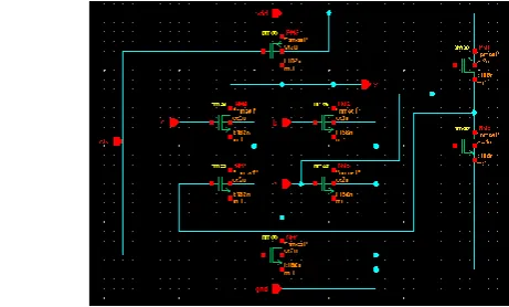
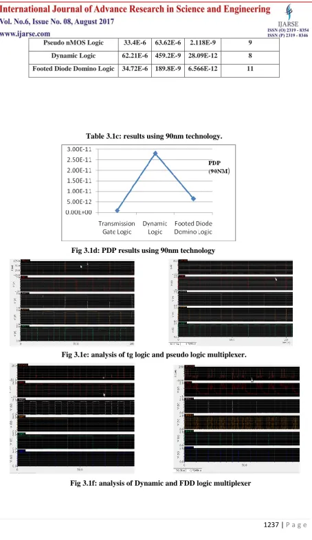
The multiplexer designs using different logics are tested on cadence tool using 180nm and 90nm technology
files. Table 3.1a, 3.1c shows the results of 180nm and 90 nm technology and fig 3.1b, 3.1d graphically shows
the same. Fig 3.1e and 3.1f shows the analysis results of all the logics.
Table 3.1a: Results Using 180nm Technology.
Fig 3.1b: PDP results using 180nm technology.
Logic Delay Power PDP Transistor Count
Transmission Gate Logic 19.95E-6 422.6E-9 8.431E-12 6
Pseudo nMOS Logic 22.33E-6 411.8E-6 9.195E-9 9
Dynamic Logic 62.219E-6 952.8E-9 59.27E-12 8
Footed Diode Domino Logic 34.72E-6 249.7E-9 8.67E-12 11
Logic Delay Power PDP Transistor Count
1237 |
P a g e
Table 3.1c: results using 90nm technology.
Fig 3.1d: PDP results using 90nm technology
Fig 3.1e: analysis of tg logic and pseudo logic multiplexer.
Fig 3.1f: analysis of Dynamic and FDD logic multiplexer
Pseudo nMOS Logic 33.4E-6 63.62E-6 2.118E-9 9
Dynamic Logic 62.21E-6 459.2E-9 28.09E-12 8
1238 |
P a g e
IV. APPLICATIONS
Multiplexers are used to send data from one location to another location. Many tasks in communication control and computer systems can be performed by multiplexers. Multiplexer are used to design digital combinational logic circuit.
Multiplexers are used in many applications such as:
Shifters and adders
Logic function generator
Look up tables
A to D converters.
V. CONCLUSIONS AND FUTURE WORK
Footed Diode Domino logic uses less power to implement a particular logic within the dynamic family. Depending upon the system requirements and application these logics may be used to design ultra low power circuits. This work shall be further carried out further to design circuits like barrel shifter for further optimisation of power, delay and area.
REFERENCES
[1] G. L .Madhumati, Dr .M .Madhavilatha and K.Ramakoteswara Rao, Power and delay analysis of a 2-to-1 multiplexer implemented in multiple logic styles for multiplexer-based decoder in Flash ADC, International Journal of Recent Trends in Engineering ,Vol 1 ,N0:4 ,2009.
[2] N. H. E. Weste and D. Harris,(2005)CMOS VLSI Design:A Circuits and Systems Perspective, 3rd Edition,Addison-Wesley, .[page.No.226].
[3] S.M. Kang and Y. Leblebici,(1999) CMOS Digital integrated Circuits- Analysis and Design, McGraw Hill,Singapore, .[page.No.350-Ch 9].
[4] A.K.Pandey,R.A.Mishraand R.K.Nagaria,(2012)Low Power Dynamic Buffer Circuits, VLSICS,Volume 3– No 5.Oct 2012, Pg 53-65.
[5]Charles F.Hawkins,(2004)CMOS Electronics, How it works and how it fails.,Jhon Wiley & Sons.[page.No.134-Ch 5].
[6] V. De and S. Borkar, “Technology and design challenges for low power and high performance,” in Proc.
Int. Symp. Low Power Electronics and Design, Aug. 1999, pp. 163–168.IEEE.
[7] M. Anders, R. Krishnamurthy, R. Spotten, and K. Soumyanath, “Robustness of sub-70 nm dynamic
circuits: Analytical techniques and scaling trends,” in Proc. Symp. VLSI Circuit, June 2001, pp. 23–24. [8]F. M. Hernandez, M. L. Aranda, V. Champac, "Noise-tolerance improvement in dynamic CMOS logic
circuits," in IEEE Proceedings Circuits, Devices and Systems, vol.153, no.6, pp.565-573, Dec. 2006. [9] K. Roy, S. Mukhopadhyay, and H. Mahmoodi-Meimand, “Leakage current in deep-submicron CMOS
circuits,” J. Circuits, Syst. Comput., vol. 11, no. 6, pp. 575–600, 2002.
[10] C. H. Cheng, S. C. Chang, J. S. Wang, and W. B. Jone, “Charge Sharing Fault Detection for CMOS
1239 |
P a g e
[11] Ashutosh Bhardwaj, Saurabh Sharma, Sanjeev Maheshwari,” Elimination of Charge Sharing Problem
in Dynamic Circuit,” International Journal of Electronics Communication and Computer Engineering
Volume 4, Issue 2.
[12] P. Ali, Asyaei, “Current-Comparision-Based Domino: New Low-Leakge High-speed Domino circuit for
wide Fan–in gates”, IEEE Transactions Very Large Scale Integration (VLSI) system, vol. 21, no. 99, 2012, pp. 934-943.
[13] H.Mahmoodi-meimand and K. Roy, “Diode-footed domino: a leakagetolerant high fan-in dynamic circuit