N A N O R E V I E W
Open Access
A Collective Study on Modeling and
Simulation of Resistive Random Access
Memory
Debashis Panda
1*, Paritosh Piyush Sahu
1,2and Tseung Yuen Tseng
3Abstract
In this work, we provide a comprehensive discussion on the various models proposed for the design and description of resistive random access memory (RRAM), being a nascent technology is heavily reliant on accurate models to develop efficient working designs and standardize its implementation across devices. This review provides detailed information regarding the various physical methodologies considered for developing models for RRAM devices. It covers all the important models reported till now and elucidates their features and limitations. Various additional effects and anomalies arising from memristive system have been addressed, and the solutions provided by the models to these problems have been shown as well. All the fundamental concepts of RRAM model development such as device operation, switching dynamics, and current-voltage relationships are covered in detail in this work. Popular models proposed by Chua, HP Labs, Yakopcic, TEAM, Stanford/ASU, Ielmini, Berco-Tseng, and many others have been compared and analyzed extensively on various parameters. The working and implementations of the window functions like Joglekar, Biolek, Prodromakis, etc. has been presented and compared as well. New well-defined modeling concepts have been discussed which increase the applicability and accuracy of the models. The use of these concepts brings forth several improvements in the existing models, which have been enumerated in this work. Following the template presented, highly accurate models would be developed which will vastly help future model developers and the modeling community.
Background
This new age of computing requires a technology being equally capable to match its growth. The new technology should be able to meet the demands of im-proved performance and scalable to cater to the future devices. Memristors, postulated in 1971 [1] by Leon O. Chua seems to fulfill these requirements and laid the foundation for new classes of devices. Memristors, short for “memory-resistors,” are basic two-terminal devices which remember their internal resistance state depending on the history of the input stimulus pro-vided. Chua devised that the memristors are characterized by a relationship between flux and charge, which are the time integrals of current and voltage, respectively.
Later in 1976, Chua and Kang [2] generalized the memristors to include in a new class of dynamical
systems called memristive systems. In the end of twentieth century, the interest in these devices had waned despite its many benefits. This was partly be-cause of the advances in silicon integrated circuit technology. But with the aging on silicon technologies and their incapability to support scaling down, the search for alternative switching devices gained attraction in the early twenty-first century. It was equally aided by the advances in the growth and characterization of nano-scale materials. This invariably leads to significant pro-gress in understanding microscopic memristive switching.
Memristor technology got a major breakthrough in the year 2008 when Strukov et al. [3] established a link between the theory and experiment for their TiOx-based
devices. Also, they obtained a pinched hysteresis in the current-voltage relationship, which is one of the identifi-able features of memristive systems [4, 5]. This opened up the memristor technology to a wide array of devices following the footprints of the metal/oxide film/metal * Correspondence:[email protected];[email protected]
1Department of Electronics and Communication Engineering, National Institute of Science and Technology, Berhampur, Odisha 761008, India Full list of author information is available at the end of the article
structure. Some of the similar types of popular devices were Oxygen RRAM (OxRRAM) [6–10] and Conductive Bridge RAM (CBRAM) [11–13] among many others. These devices are generally classified on the basis of their switching mechanism.
Resistive Random Access Memory (RRAM)
Research interest into these emerging devices heightened because the non-volatile memristive behavior demon-strated could be harnessed into non-volatile memory. They are being seen as potential alternatives of the flash memory technology. With present age computing being more and more data driven, there has been demands for a memory technology which is more in-tune with the present and future requirements. Compared to the sev-eral emerging devices, RRAM devices are more scalable [14–18], have high density [19–24], consume low power [25–29], are faster [30–33], have higher endurance and retention [34–37] and highly CMOS compatible [38–42]. RRAM devices are one of the most popular non-volatile memory technologies with extensive study being undertaken to understand their mechanism and de-velop models to realize the device operation and design accurate and simple device structure. The devices are sim-ple two-terminal metal-insulator-metal (MIM) structure and switch between two resistance states low-resistance state (LRS) and high-resistance state (HRS). A LRS sug-gests the device is in the SET or ON state. A contrasting HRS means the device is in the RESET or OFF state. Through this switching of resistance states in the de-vice, the data bit is stored [43–45]. RRAM devices can be classified into bipolar and unipolar devices, depending on the polarity of switching. In unipolar switching, the devices switch in the same polarity bias, whereas in bipolar switching, bias of both the polarities is required.
Several approaches have been proposed to explain the switching mechanism of RRAM devices, but the most popular and widely accepted, for binary oxide-based RRAM devices, is the formation and ruptured of local-ized conductive filaments (CF) by the drift of oxygen ions/ vacancies [9, 16, 46–49]. The SET/RESET occurs as a result of the combination/re-generation of the oxy-gen ions/vacancies [50–52]. It has been demonstrated that the performance of the RRAM devices is strongly affected by the choice of the active oxide layer [53–55]. A variety of oxide systems such as HfOx, TiOx, NiOx,
TaOx, ZnOx, etc. [56–66] have been used to
demon-strate resistive switching behavior. There have been some controversies whether RRAM devices are actually memristive devices. To make the position of RRAM de-vices clear, Chua provided clarifications that they are indeed memristive devices [67].
Importance of RRAM Modeling
A very important aspect of developing electronic de-vices based on new semiconductor technologies is the role of modeling. An accurate and comprehensive model is of paramount importance in understanding the device operation, designing it for optimum per-formance, and verifying that it matches the required specifications. A number of models have been proposed with varying degrees of accuracy, different features, and mixed results. So, any developer aiming to design a ro-bust and flexible model for RRAM devices should have information about the methods tried before and the constraints faced.
In this work, we have discussed in detail all the fea-tures and characteristics of the various RRAM models. General memristor models are also considered to ex-plain RRAM devices [67]. Starting from the Chua model [1] which provides the basics of memristors, we discuss the fundamental definition of memristors. The break-through for memristors and RRAM devices provided by the HP model [3] is discussed in detail. Linear ion drift effects, which form the basics of the mechanism of these devices, along with the non-linear effects [46, 68, 69], are considered. The Pickett-Abdalla model [70–72] which laid the foundation for SPICE compatible physics-based models is covered in-depth. Its various features which have been adopted and refined by the Yakopcic model [73, 74] are also covered.
Models which introduced new features such as thresh-old effects [75–77], taking filament gap as the state vari-able [78–81], have been reviewed. Some of the models which account for unipolar devices and temperature ef-fects [82–84] are reviewed in detail. Also considered are physical models [85, 86] based on the device growth dynamics. Along with these, models considering only bi-polar devices [87–89], change of CF size [90, 91], and many other factors [92, 93] are taken into account. A concise analysis of all the discussed models has been presented in Table 1.
models has been divided into those that describe bipo-lar devices and unipobipo-lar devices. Window function im-plementation models are described in a separate section.
Earlier, there have been multiple reviews on RRAM device mechanisms [46, 101–105], fabrication technol-ogy [106–109], material stacks [110–113], and a concise discussion on some of the models present at that time [114]. Very recently Villena et al. [115] combined the theory of all RRAM modeling and proposed an optimize model. In this study, we focused more on the various modeling techniques along with the solutions provided to various drawbacks. A comprehensive discussion on boundary condition models which can be classified as pseudo-compact models have also been discussed. Some critical modeling techniques have been investigated in this work which can significantly help model developers. Also, a discussion on various simulation techniques and platforms for RRAM models such as SPICE [116, 117] has been included which is highly essential. Our work
aims to fill a significant gap in the RRAM modeling community.
RRAM Models for Bipolar Devices
Chua Model
Leon O. Chua in 1971 put forward the idea of memristor [1] that it was indeed the fourth basic element alongside the resistor, capacitor, and inductor. The basic charac-teristics of a memristor are believed to be flux con-trolled (φ) or charge controlled (q) and are defined by a relation of the type g (φ,q) = 0.
Chua defined the voltage of a memristor as [1]:
v tð Þ ¼M q tð ð Þi tð ÞÞ ð1Þ
where
M qð Þ ¼dφð Þq =dq ð2Þ
[image:3.595.60.540.99.472.2]The current flowing through a flux-controlled memris-tor was formulated as1:
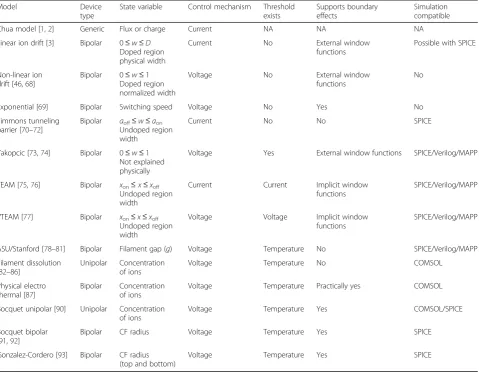
Table 1Comparative analysis of the models
Model Device
type
State variable Control mechanism Threshold exists
Supports boundary effects
Simulation compatible Chua model [1,2] Generic Flux or charge Current NA NA NA Linear ion drift [3] Bipolar 0≤w≤D
Doped region physical width
Current No External window functions
Possible with SPICE
Non-linear ion drift [46,68]
Bipolar 0≤w≤1 Doped region normalized width
Voltage No External window functions
No
Exponential [69] Bipolar Switching speed Voltage No Yes No Simmons tunneling
barrier [70–72]
Bipolar aoff≤w≤aon Undoped region width
Current No No SPICE
Yakopcic [73,74] Bipolar 0≤w≤1 Not explained physically
Voltage Yes External window functions SPICE/Verilog/MAPP
TEAM [75,76] Bipolar xon≤x≤xoff Undoped region width
Current Current Implicit window functions
SPICE/Verilog/MAPP
VTEAM [77] Bipolar xon≤x≤xoff Undoped region width
Voltage Voltage Implicit window functions
SPICE/Verilog/MAPP
ASU/Stanford [78–81] Bipolar Filament gap (g) Voltage Temperature No SPICE/Verilog/MAPP Filament dissolution
[82–86]
Unipolar Concentration of ions
Voltage Temperature No COMSOL
Physical electro thermal [87]
Bipolar Concentration of ions
Voltage Temperature Practically yes COMSOL
Bocquet unipolar [90] Unipolar Concentration of ions
Voltage Temperature Yes COMSOL/SPICE
Bocquet bipolar [91,92]
Bipolar CF radius Voltage Temperature Yes SPICE
Gonzalez-Cordero [93] Bipolar CF radius (top and bottom)
i tð Þ ¼Wðφð Þt v tð ÞÞ ð3Þ
where
Wð Þ ¼φ dqð Þφ =dφ ð4Þ
Here, the parametersM(q) andW(φ) are defined as in-cremental memristance and inin-cremental memductance, respectively, owing to them having units similar to re-sistance and conductance. The φ-q curves for the three memristor devices are shown in Fig. 1. These curves are
generated by a basic memristor-resistor (M-R) circuit which gives rise to three types of memristors. The φ-q
variance for those devices is shown in Fig. 1a–e, respect-ively. Figure 1b–f depicts the correspondingI-Vrelations of the same three memristors.
The equations presented above can be simplified into the following [1]:
v¼R wð Þ i ð5Þ
a
c
e
b
d
f
[image:4.595.61.535.199.721.2]dw
dt ¼i ð6Þ
wherewis the state variable of the device andRa gener-alized resistance that depends upon the internal state of the device.
The value of incremental memristance (memductance) at a time instant t0depends on the time integration of the complete memristor current (voltage) fromt=−tto
t=t0. So, this translates to the fact that while a memris-tor acts as a normal resismemris-tor at any instant of time t0, but its resistance (conductance) values depend on the complete past history of the device current (voltage), hence the justification of the name memory resistor.
Interestingly, at the time of specified memristor volt-agev(t) or currenti(t), the memristor behaves as a linear time-varying resistor. But in the case when theφ-qcurve is a straight line, i.e.,M(q)= RorW(φ)= G, the memris-tor acts like a linear time-invariant resismemris-tor. So, a mem-ristor device cannot be used in linear network theory but can be used to define circuits where the present state of the parameters is dependent on the past states.
Later, in 1976, Chua and Kang [2] generalized the memristor concept to include memristive systems which include many non-linear dynamic systems. It was de-scribed by the equations [2]:
v¼R wð ;iÞ i ð7Þ
dw
dt ¼f wð ;iÞ ð8Þ
wherewis defined as a set of state variables,Randfare explicit functions of time. A basic difference between memristors and memristive systems is that in the later the flux is no longer uniquely defined by the charge. Memristive systems can be distinguished from a general dynamic system in that there is no current flowing in the device when the voltage drop across it is zero.
The memristor equations were used reasonably to de-fine the variable state of a threshold switch by Chua [1], which are the first instance of using memristors in de-vice modeling. Formulation of the memristor by Chua rightfully laid the foundation for a new class of devices and varied applications which use a basic circuit element to store data. This basic concept of memristors led to the design of new architectures for future non-volatile memory applications of which RRAM is a promising candidate. There has been significant amount of theories explaining the working of RRAM devices and models defining them, which are fundamentally based on the memristor model.
A very interesting application of the flux-charge model is its use [118] to define a unipolar RRAM and implement it in SPICE. Owing to the simplicity
of the flux-charge equations, they can be easily inte-grated into circuit simulators with few modifications. SPICE model was tested against experimental data of HfO2-based unipolar RRAM device. The non-linear relation proposed to fit the experimentally obtained normalized q-φ values is given as [118]:
qð Þ ¼φ qr min 1; φ
φr
n
ð9Þ
Here, φr is the flux at the RESET point. When this
value q(φ) =qr is obtained, the CF disappears and the current associated with the CF is set back to 0. This translates to the device being in the HRS. To investigate the ability of the model to reproduce unipolar switching characteristics of the device, a standard bias sweep oper-ation is performed. The voltage applied on the device at reset state is increased progressively from zero bias until it reaches the LRS and then the bias is swept back to zero volts. The LRS current is modeled using a modified form of the current relation of the Chua model [1], given as [118]:
i tð Þ ¼ K ffiffiffi φ
p
v tð Þ ifφ<φr
0 ifφ¼φr
ð10Þ
HRS current is assumed to be controlled by a thermi-onic emission, so the current in that state is modeled as:
i vð Þ ¼IA e
v vA−1
ð11Þ
Threshold effects are also considered in the model. It has been assumed that the threshold voltage effect arises due to contact effects. It can be taken into account by including a voltage threshold for the flux computation in both the SET and RESET processes. The modified current is given by [118]:
i tð Þ ¼ IA e v vA
−1 0 B B @
1 C C
A ifφ<φs
Kpffiffiffiφv tð Þ ifφ<φr 8
> > > > < > > > > :
ð12Þ
Here, ϕrandϕs are the RESET and SET flux,
Linear Ion Drift Model
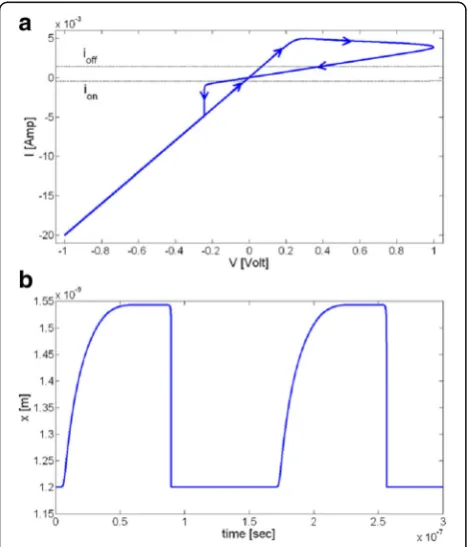
With a considerable gap in the consequent decades after the formulation of the memristor by Chua, researchers at HP Labs [3] in 2008 made an exciting find regarding mem-ristor devices. Although Chua had formulated the presence of an element such as a memristor, there had not been a realizable circuit or model developed after that although several efforts were reported to fabricate RRAM devices in the very beginning of twenty-first century. The team at HP Labs led by Strukov et al. [3] realized a functional nano-scale memristive system where memristance occurs natur-ally, where solid-state electronic and ionic transport are coupled together under an external voltage bias. Those sys-tems show a hysteretic relation between the current and voltage characteristics similar to other nanoscale electronic devices, thus leading to a fundamental understanding of memristive systems and the design of similar systems.
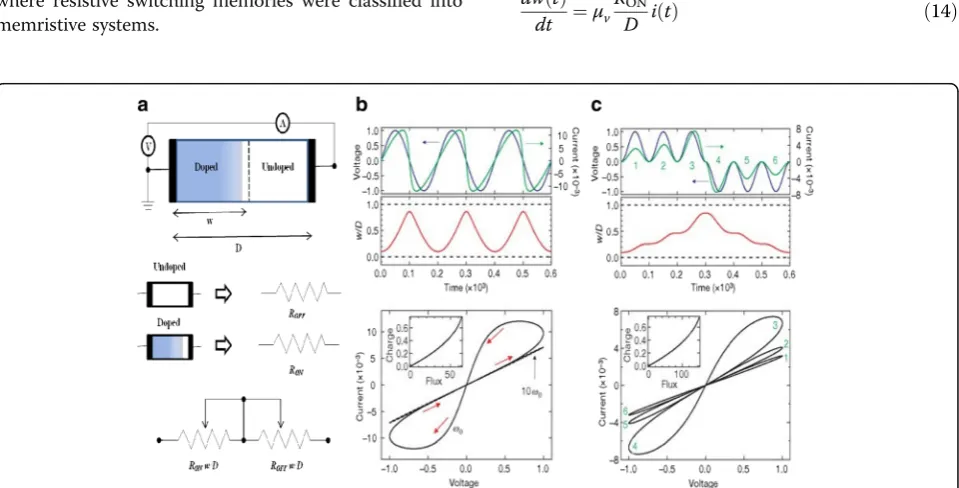
A simple two-terminal device was reported, where an oxide (TiO2) of thicknessDwas sandwiched in between two Pt electrodes. Hysteresis I-Vswitching curves have been compared with the simulated curve. Although the exact mechanism of these devices was not completely understood at that time, it was one of the first instances where resistive switching memories were classified into memristive systems.
A schematic device structure of TiO2-based memristor is shown in Fig. 2a [3], where there are two variable re-sistances in series, called asRONwhich is the low resist-ance in the semiconductor region with higher dopant concentration. A lesser dopant concentration makes the other part higher in resistance, called as ROFF. Relation between the applied voltagev(t) and current through the system i(t) owing to ohmic electronic conductance and linear ionic drift in a uniform field with average ion mo-bility is given by [3]:
v tð Þ ¼ RONw tð Þ
D þROFF 1− w tð Þ
D
i tð Þ ð13Þ
Although the equation above itself is non-linear, the resistance of the device linearly changes with the ap-plied voltage v(t), thus the attribution of linearity to the model. Device defined by Strukov et al. [3] acts as a perfect memristor for only a particular bounded range of the state variable w. The state variable is de-fined as [3]:
dw tð Þ dt ¼μv
RON
D i tð Þ ð14Þ
Fig. 2The coupled variable-resistor model for a memristor is presented.aA simplified equivalent circuit comprising of a (V) voltmeter and (A) ammeter.b,cThe applied voltage (blue) and resulting current (green) as a function of timetfor a typical memristor are also presented. Inbthe applied voltage isv0sin(v0t) and the resistance ratio isROFF/RON= 160, and incthe applied voltage is ±v0sin2(ω0t) andROFF/RON= 380, whereω0 is the frequency andv0is the magnitude of the applied voltage. The numbers 1–6 are labeled for successive waves in the applied voltage and the corresponding loops ini–vcurves. In each plot, the axes are dimensionless, with voltage, current, time, flux, and charge expressed in units of
v0= 1 V,i0≡v0/RON= 10 mA,t0≡2π/ω0≡D2/μvv0= 10 m/s,v0t0andi0t0, respectively. The termi0denotes the maximum possible current through the device, andt0is the shortest time required for linear drift of dopants across the full device length in a uniform fieldv0/D, for example withD = 10 nm andμV= 10−10cm2s−1V−1. It is to be noted that for the parameters chosen, the applied bias never forces either of the two resistive regions to collapse; for example,w/Ddoes not approach zero or one (shown with dashed lines in the middle plots inbandc). Also, the dashed
[image:6.595.59.539.368.612.2]Memristance of the system proposed by Chua [1] in Eq. (1) is defined by using the above two Eqs. (13) and (14) [3]:
M qð Þ ¼ROFF 1−μv
RON
D2 q tð Þ
ð15Þ
In the above Eq. (15), theq-dependent term is the pri-mary contribution to memristance. An interesting ana-lysis provided as to why this particular phenomenon was hidden for so long is due to that magnetic field did not play an explicit role in the mechanism. For a memristor to be realized in simple terms, there should exist a non-linear relationship between the integrals of voltage and current.
The Eqs. (13)–(15) also incorporate the fundamentals of bipolar switching, that is the device switches from one state to another by the application of voltage of two polarities. As a result, devices showing bipolar hysteretic
I-Vrelationships are capable of being modeled by these equations, and hence leading to the classification of such devices as memristive systems. Such behavior is observed in many material systems such as organic films [119–123], chalcogenides [124–126], metal oxides [127–129], dielectric oxides [130–132], perovskites [133–136], etc. The HP team themselves used a TiO2 [3] system and observed similar bipolar switching char-acteristics, with the dopant or impurity motion through the active region as the reason for such dramatic changes in the resistance. This is shown in Fig. 2b, c with the
current showing drastic drop and rapid rise with the change in voltage.
Physically, the active region in these two terminal de-vices operates within the bound, 0 toD, the thickness of the oxide layer, so the state variable w is also bounded between the thicknesses. Figure 3 indicates the variation of w/D with time for the parameter never leaving the bounds of 0 andD[3]. The sudden change in resistance or the switching is caused by the devices reaching these bounds. In order to model this condition, suitable boundary conditions are used. Certain anomalies are ob-served in the device at the boundaries specifically. There is a non-constant change in the rate of the dynamic state variables over the available change. Also, the ion mobil-ity is significantly less at the boundaries than in the mid-dle. This is attributed to the non-linear dopant drift effects at the boundaries. Therefore, to properly account for these effects, the variations of certain window func-tions are used to define the bounds for the devices. HP team proposed a window function multiplied to the state variable Eq. (9) given as [3]:
f xð Þ ¼wð1−wÞ .
D2 ð16Þ
This model could be attributed to laying the founda-tions for future RRAM models. It can also be used for two terminal semiconductor devices having bipolar hys-teretic I-V relationships. Taking the mechanism of a memristor as the reference, numerous future models for RRAM devices have been developed.
Fig. 3Simulated voltage-driven memristive device.aSimulation with dynamic negative differential resistance.bSimulation with no dynamic negative differential resistance.cSimulation governed by nonlinear ionic drift. In the upper plots ofa,b, andc, the voltage stimulus (blue) and the corresponding change in the normalized state variablew/D(red) is plotted against time. In all cases, hard switching occurs whenw/Dclosely approaches the boundaries at zero and one (dashed), and the qualitatively differenti-vhysteresis shapes are due to the specific dependence of
[image:7.595.58.538.474.675.2]Non-linear Ion Drift Model
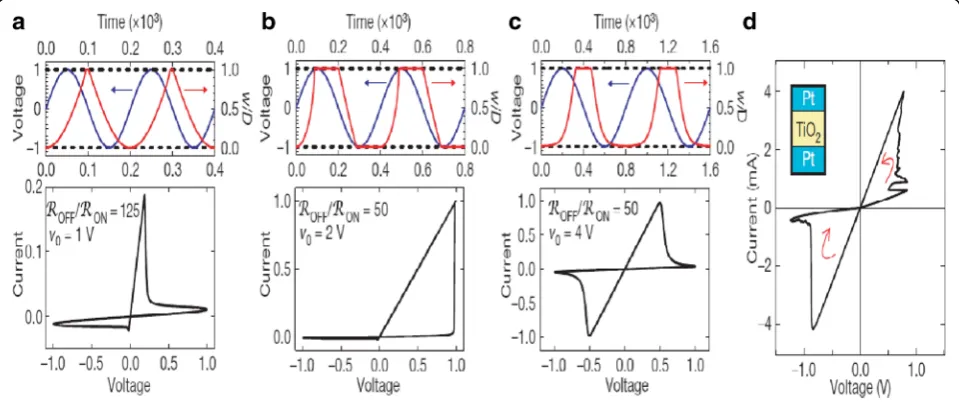
Linear ion drift model developed by HP [3] primarily demonstrated linear drift effects in the bulk region of the memristor device. They observed some non-linear effects at the boundaries but did not define it compre-hensively. Non-linear dependence of the dopant drift on applied voltage was observed and formulated by Yang et al. [46] in 2008. They proposed a current-voltage relationship accounted for the non-linear effects accurately. It was later improved and added upon by Eero Lehtonen and Mika Laiho [68].
Conduction in memristive devices is controlled by a spatially heterogeneous metal/oxide electronic barrier was reported by Yang et al. [46]. The switching is caused by the drift of positively charged oxygen vacancies acting as native dopants to form or dissolute conductive chan-nels through this electronic barrier. The concentration of vacancies is higher at the boundaries or metal/oxide interfaces. The ON and OFF switching took place at the top interface only, which indicates that top electrode acts as the active electrode.
[image:8.595.306.539.86.415.2]The effect of oxygen vacancies on the switching char-acteristics of titanium oxide-based memristor is shown in Fig. 4 [46].The samples having different oxygen vacancies with different layer sequences of TiO2 show opposite switching defined by their polarities. Also, the addition of extra vacancies to the top interface, shown in Fig. 4c, changes the switching curves thus confirming the dominant role of non-ohmic interfaces in memristive devices. This forms the basis of the non-linearity effects that originate at the interfaces and govern the device switching.
Yang et al. [46] explained the above fact that the mem-ristive devices act as dynamic resistors which change their state according to the time integral of the applied current or voltage; they failed to give a relationship de-scribing a dynamic state variable. The proposed current-voltage relationship can be described as [46]:
I¼wnβsinhð Þ þαv χðeγv−1Þ ð17Þ
Here, β, γ, n, and χare fitting constants. In the above equation, the first term βsinh(αv) approximates [1] the ON state of the memristor where the electrons tunnel through the thin residual electronic barrier.wis defined as the state variable of the device in the range of 0 (OFF) and 1 (ON). Second part of the equation approxi-mates the OFF state of the device with the other param-eters acting as fitting constants. Parameternhere acts as the free parameter used to modify the switching between the states. During the adjustment ofn,the non-linear ef-fects come into picture. I-V curve from the fabricated device is modeled using the Eq. (16). The best fitting is obtained at 14≤n≤22. This can be interpreted as
evidence that the effective vacancy drift velocity depends in a very highly non-linear way with the applied voltage to the device. So, the majority of the dopant drift effects at the boundaries/interfaces could then be understood as non-linear in nature.
A relationship describing the dynamics of the state variablewin this model using SPICE [116, 117] was pro-posed by Lehtonen and Laiho [68]. The time derivative ofwwas modeled as [68]:
dw
dt ¼af wð Þ g vð Þ ð18Þ
Here, ais a constant, f: [0, 1]→Ris a proposed win-dow function and g: R→R is considered a linear func-tion proposed earlier in the linear drift model (where R
stands for real numbers). The authors demonstrated
from the solutions that in order to imitate the working of the memristor proposed by Yang et al. [46],g(v) must be a non-linear, odd, and monotonically increasing function. A non-linear function which was proposed was [68]:
g vð Þ ¼vq ð19Þ
Here, the exponent q is used to mimic the rapid switching process. Transition between ON and OFF state in a memristor generally takes place very fast. An input voltage with a very high sweep rate is used to ob-tain such behavior. This is the first implementation of memristor models in the SPICE platform [116, 117].The major advantage of SPICE implementation is the ability of the model to be used in analog circuits and simula-tions and can be verified as fit to be circuit implementa-ble or not. Although many improvements were made in subsequent models, this model lays the foundation for the rest of the RRAM models by accurately taking into consideration and explaining the non-linear dopant drift effects [3, 46].
Exponential Ion Drift Model
In practice, resistance switching characteristics are non-linear in nature. To analyze such exponential character-istics, Strukov et al. [69] proposed exponential ion drift model in 2009. This non-linearity caused a significant variation in retention time and write speed. Due to the exponential dependence of the switching rate for high electric field, the exponential ion drift model is general-ized to explain the phenomenon by the non-linear microscopic drift of charged species in the dielectric at high field and temperature.
The major factors considered for this model are switching speed and volatility. Switching speed is the time required for the device to switch from one resist-ance state to the other, i.e., it can be deemed as the time required to writing the data into the memory and is de-noted asτwrite. Volatility is the time required for the de-vice to lose its resistance state, i.e., the time taken to store the data into the device before erased denoted as
τstore. The ratio between τstore and τwrite derived using the Einstein-Nernst formula is given by [69]:
τstore=τwriteELμ=D¼qEL=kBT ð20Þ
Here, L is the length of the device with an active doped region D and kB the Boltzmann constant. Ratio between the two parameters is approximately three orders of magnitude when considered at room temperature and reasonable bias voltages. Such a high volatility to switch-ing speed ratio suggests a strong non-linear ionic trans-port due to drift-diffusion inside the device. For high-field ionic drift, the overall effect on the average drift velocity of the ions is given by the model as [69]:
ν≈feape−
Ea
kBT sinhqEap=2kBT
ν¼ −μE; E≪E0
μE0eE=E0; EE0
(
ð21Þ
Here, ν is the drift velocity, fe the frequency of escape attempts, T the device temperature, ap the periodicity, Ea the activation energy, and E the ap-plied electric field.
Variation of the drift velocity with the applied electric field is shown in Fig. 5 [69]. The exponential variation can be clearly seen at high applied fields which lend non-linearity to the model. There are a few shortcom-ings for this model which affect its accuracy and also the calculation of the average drift velocity mentioned in Eq. (20). This model is primarily suited for application to ionic crystals where the major interaction forces are the Coulomb repulsion and van-der-Waals forces. Its appli-cation for covalent crystals will affect the accuracy of calculation due to the complex interactions of electrons and ions in high electric field. Also, electrochemical dif-fusion reactions and redox reactions are not explained by the model [91–93]. This can cause significant issues in the systems where the physical switching mechanism is governed by electrochemical processes.
Simmons Tunneling Barrier Model
Though Lehtonen and Laiho [68] first proposed SPICE-based simulations model for non-linear ion drift model as mentioned in the “Non-linear Ion Drift Model” sec-tion, but this modeling is not suitable for use in an electrical-based time domain simulation, due to the lack of proper definition of simulation parameters and equa-tions. This situation changed with the Pickett-Adballa et al. [70–72] model where a new class of model based on
[image:9.595.306.539.550.694.2]the device physics was demonstrated, which is capable of being explained and compatible with SPICE. The equations were modified to fit the requirements for SPICE implementation.
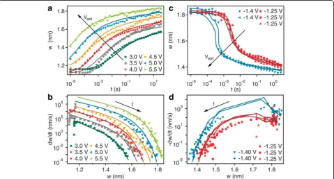
The analysis was based on the results from a TiO2 -based memristor device [70] where the tunneling bar-rier width w was considered to be the dynamic state variable. This later set the precedent for one of the most popular parameters being treated as the dy-namic variable in memristor systems, the other being the length of conductive filament inside the dielectric media. The deduction based on their analysis was that the dynamic behavior for on and off switching of the devices was highly non-linear and asymmetric as can be seen in Fig. 6 [70]. The explanation provided for the deduction was the exponential dependence of the drift velocity of ionized dopants on the applied current or voltage.
The current in the device was explained based on the Simmons tunneling barrier I-V expressions [137], and based on this analysis, the dynamic state variable was determined to be the Simmons tunnel barrier width (w). The current was given as [72]:
i¼ j0A
Δw2 ϕbe
−B ffiffiffiffiϕb
p
−ðϕbþe vj jÞe−B ffiffiffiffiffiffiffiffiffiffiffiffi
ϕbþe vj j
p
n o
ð22Þ
where
j0¼ e
2πh;w1¼
1:2λw
ϕ0
;Δw¼w2−w1 ð23Þ
ϕI¼ϕ0−vg
w1þw2
w
− 1:15Δwλw
ln w2ðw−w1Þ w1ðw−w2Þ
ð24Þ
B¼4πΔw10 −9pffiffiffiffiffiffiffiffiffi2me
h
ð25Þ
w2¼w1þw 1−
9:2λ 3ϕ0þ4λ−2jvgj
!
ð26Þ
λ¼ e: ln 2ð Þ
8πεε0w10−9
ð27Þ
The parameters have been adjusted here such that the barrier height φb is in volts (not in electron volts), and
the time-varying tunnel barrier width w is in nanome-ters. In the equations above, Ais the channel area of the
[image:10.595.59.539.394.652.2]memristor,eis the electron charge,his the Planck’s
con-stant, εis the dielectric constant,mis the mass of elec-tron, φ0 is a standard barrier height taken from reference [70], andvis the voltage across the tunnel bar-rier.Bis a fitting constant. In lieu of the analytical form of the equations, they can be conveniently described and implemented in SPICE, or it can be implemented with the any SPICE compatible electrical simulator.
The dynamic state variablewvaries with time as [72]:
dw
dt ¼f1 sinh
jij i1
expð−exp w−a1
wc −
jij b
−w
wc
ð28Þ
This is in the case of off switching state (i > 0). Whereas foron switching state(i <0), the state variable varies as [72]:
dw
dt ¼−f2 sinh
jij i2
expð−exp a2−w
wc −
jij b
−w
wc
ð29Þ
Here,f1,i1,a1,b,wc,f2,i2, anda2are fitting parameters. The abovementioned equations are used to model the memristor on the circuit level considering the electron tunnel barrier as a voltage-dependent current source, and the conducting channel (TiO2) is modeled as a series resistance. The voltage drops across the tunnel barrier and the series resistance make up the complete voltage drop across the circuit.
The dynamic behavior of the device is visibly complex as it is physics-based modeling approach and has been articulated as such by the Eqs. (27) and (28). The rate of switching possibly has contributions from the nonlinear drift at high electric fields and local Joule heating of the junction speeding up the thermally activated drift of oxygen vacancies [16, 46, 82, 83]. This can be clearly seen in the case of Fig. 6a, c [70] where the nature of the curves at high electric fields is quite different to those in low fields. The switching in the device is directly affected by the width of the gap. Application of a positive bias on the top electrode increases the state variablewresulting in an exponential increase in the resistance of the device as illustrated in Fig. 6b, d [70]. An opposite phenomenon occurs when negative bias is applied on the top elec-trode. This signifies the bipolar nature of the switching characteristics and their dependence on the dynamic state variablew.
The SPICE simulation of the model equations is illus-trated in Fig. 7 [72]. The experimental data from the fab-ricated device is plotted against the simulatedI-Vcurves showing a good fit between the two. This implementa-tion paves the way for future SPICE simulaimplementa-tions of RRAM devices [74, 77, 81]. A possible shortcoming in
this model is the lack of a boundary for the dynamic variable and a threshold voltage within which the model should work. The growth of tunneling barrier width w
can possibly go to unlimited quantities owing to the lack of a bound for the same, thus creating non-realizable sce-narios for the device mechanism. Many models have employed what is called a window function to define the limits for the defined dynamic state variable in the model.
Yakopcic Model
Although not validated specifically for RRAM devices at the time of development, the Yakopcic model [73, 74] closely resembled a variety of RRAM devices. The model was initially tested for TiO2systems [73], and these sys-tems are indeed one of the most popular ones along with HfO2-based RRAM devices.
This model was based on the Pickett-Adballa model [70–72] using a similar state variable, but it was modi-fied to include neuromorphic systems as well. It was one of the first models to consider the functioning of synap-ses into their equations. This model was verified for the device used by the HP lab team to explain the working of memristive systems.
The state variable w(t), a value between zero and one considered here, directly affected the current through the device and also the dynamics of the device, i.e., the resistance. The current in the device is given as [73]:
I tð Þ ¼ a1w tð Þsinhðbv tð ÞÞ; v tð Þ≥0 a2w tð Þsinhðbv tð ÞÞ; v tð Þ<0
ð30Þ
Two functions, namely g(v(t)) and f(x(t)), are respon-sible for the change in the state variable. a1, a2, and b
Fig. 7Experimental data (black dots) and corresponding simulated
[image:11.595.304.540.87.258.2]are fitting constants. Change of the state of the variable is generally governed by a threshold voltage, i.e., there is a physical change in the device structure above a certain threshold voltage. The function g(v(t)) here models the ON and OFF voltages of the device which also takes into account the polarity of the input voltage. This results in a better fit to the experimental data in case of bipolar switching where the values of set (vp) and reset (vn) volt-age, i.e., the thresholds are different. It is defined as [73]:
g v tð ð ÞÞ ¼
Ap ev tð Þ−evp
; v tð Þ>vp
−An e−v tð Þ−evn
; v tð Þ<−vn 0; −vn≤v tð Þ≤vp 8
> > < > > :
ð31Þ
ApandAnindicate the rate of the change of state once the voltage threshold is crossed. It can be understood as the dissolution or the rupture of the filament in terms of RRAM devices. There is in-built support for threshold values in the model, which enhances its applicability.
The state change variable modeled by the function
f(w(t)) is used to define the boundaries for the variable. It explains the motion of the charge carrying particles based on the threshold values, also adding the possibility to define the motion of the particles based on the polarity of the input voltage. This basically acts as a window func-tion which restricts the state change variable within cer-tain boundary given as [73]:
f wð Þ ¼ e
−αpðw−wpÞf
p w;wp
; w≥wp
1; w<wp
(
ð32Þ
f wð Þ ¼ e
αnðwþwn−1Þf
nðw;wnÞ; w≤1−wn
1; w>1−wn
(
ð33Þ
Here, fp(w,wp) is a window function which limits the value off(w) to 0 whenx(t) = 1 andv(t) > 0.fn(w,wn) is a similar window function which does not allow the value of w(t) to become less than zero when the current flow is reversed.
The window functions are defined as [73]:
fp w;wp
¼wp−w 1−wpþ
1 ð34Þ
fnðw;wnÞ ¼ w
1−wn ð
35Þ
The movement of dynamic state variable, in simple words, the rate of switching, is governed by a differential equation. The growth and decay of the tunneling barrier
width are the defining mechanism for this particular model, and it is given by [73]:
dw
dt ¼g v tð ð ÞÞf w tð ð ÞÞ ð36Þ
Owing to the analytical nature of the coupled equa-tions, they can be solved using a mathematical solver such as MATLAB [138, 139]. The differential equa-tion can also be solved in MATLAB using the in-built solvers idt() and ddt() functions, which employ the time step integration method. This particular model was simulated using the characterization data of the TiO2 memristor from HP Labs [3], and the fit-ting obtained was pretty good when the fitfit-ting pa-rameters are properly calibrated.
A separate SPICE implementation of the same model was reported by Yakopcic et al. [74] which were fitted and characterized for a multitude of de-vices for both sinusoidal and repeated sweep inputs. The SPICE implementation revealed a good accuracy and applicability of the model at the circuit level. The model was correlated with a variety of experimental data, and low error rates of about 6% were obtained. It was one of the first SPICE implementation where the model was tested under sinusoidal as well as re-petitive sweeping inputs. This helps in determining the AC behavior of the device. Along with that, very important device variability analysis is performed which defines the error tolerance in the device. Vari-ability is an important issue, when the RRAM device is used in large systems, such as arrays. The variabil-ity analysis performed is essential in knowing until which point the system can tolerate the variability. After reaching the critical point, there is possibility of errors in device read/write.
when it comes to circuit level SPICE simulations, vari-ability analysis, and read/write operation simulations for RRAM devices.
TEAM/VTEAM Model
Threshold Adaptive Memristor (TEAM) model [75, 76] builds based on the Simmons Tunneling Barrier model [70–72] (discussed in the “Simmons Tunneling Barrier Model” section) and delivers a much simpler physics-based modeling approach for memristive systems. I-V
relationship in this case is not fixed and can be chosen to fit any device which provides some amount of flexibil-ity in the model. TEAM model arose from the need of simpler analytical equations which describe the mechan-ism of memristive systems accurately and which take less computation time.
This model is based on the approximation of the high non-linear dependence of the memristive device current; the device can be modeled as a device with threshold currents. The results are evident in Fig. 8. As with the tunneling barrier model, the internal state derivate is dependent on the current and the state variable itself, which is the effective tunnel width. It can be modeled effectively by [76]:
dw tð Þ dt ¼
koff
i tð Þ ioff −
1
0 @
1 A
αoff
foffð Þw; 0<ioff<i
0; ion<i<ioff
kon
i tð Þ ion−
1
0 @
1 A
αon
fonð Þw ; i<ion<0
8 > > > > > > > > < > > > > > > > > :
ð37Þ
Variation of the state variable with time is asymmet-rical in nature, as shown in Fig. 8b. This means that the ON and OFF switching times are not equal. In the Eq. (36), ionand ioffact as the current thresholds. Functions fon and foff are window functions which bound the in-ternal state variablex(t) within [won,woff]. Window func-tions are described as [76]:
foffð Þ ¼w exp −exp w−aoff
wc
; ð38Þ
fonð Þ ¼w exp −exp −w−aon
wc
; ð39Þ
The window functions describe the dependence of the derivative in the state variable x. They work well within the described boundaries, but the problem arises when the device goes beyond the boundaries. There are no limiting parameters here, and the window function only describes the state variable inside a particular limit. If the device goes beyond the boundaries, it can cause con-vergence issues with the simulator and it does not make sense for good modeling practice in case of analog devices.
I-Vrelationship in this model is derived from the tun-neling barrier model, as discussed in the“Simmons Tun-neling Barrier Model” section. Due to the non-linear nature of the tunneling current, the change in resistance varies exponentially with the state variable. So, it is as-sumed that any change in the tunnel barrier width changes the memristance in an exponential manner which deduces to [76]:
v tð Þ ¼RONeðλ=woff−wonÞðw−wonÞi tð Þ ð40Þ
Here, λ is a fitting parameter and RON the equivalent effective resistance at the bounds.
I-V relationship for this model can be seen in Fig. 8a [76]. Although there is a presence of a pinched hyster-esis, the form and structure of the curve are not well-defined. The model is driven with a sinusoidal input of 1 V. The verification done for this model is different from the tunneling model [70–72] in terms of the plat-form used to simulate it. The latter model uses a SPICE macro model [72] to describe the equations, but SPICE takes up a significant amount of computation time.
Fig. 8A sinusoidal input of 1 V applied to the TEAM model using the same fitting parameters as used in Fig. 10 [76]. The values of
[image:13.595.57.292.391.665.2]Modeling in Verilog-A [140–143] is much more effi-cient, and the TEAM model [75] utilizes this functional-ity to model the equations presented by them.
A slightly modified version of the TEAM model with the introduction of voltage threshold levels was reported by the same group, called Voltage Threshold Adaptive Memristor model (VTEAM) [77]. Discussed TEAM model was based on threshold currents, whereas VTEAM is based on threshold voltages. The major ad-vantages cited for using threshold voltages is that com-parison with current causes performance and reliability issues if the condition is not satisfied, i.e., a low-current threshold will automatically have a low-voltage threshold as well. This might affect the overall performance of the device. Also with a threshold voltage, there is no risk with going overboard with high power and voltage destroying the device as the values are automatically controlled.
The VTEAM follows a similar concept to the TEAM model, being based on an expression of the derivative of an internal state variable. The current is dependent on the state variable itself. The only difference is inclusion of a threshold voltage. The internal state variable (w) is defined as [77]:
dw dt ¼
koff
v tð Þ voff−
1
0 @
1 A
αoff
foffð Þw; 0<voff<v
0; von<v<voff
kon
v tð Þ von−
1
0 @
1 A
αon
fonð Þw; v<von<0
8 > > > > > > > > < > > > > > > > > :
ð41Þ
Similar to the TEAM model, the functionsfonandfoff act as window functions which bound the internal state variable w within [won, woff]. As has been assumed in the model, current varies exponentially with the in-ternal state variable on most occasions which is defined by [77]:
i tð Þ ¼e
− λ
woff−wonðw−wonÞ
RON
v tð Þ ð42Þ
The comparative analysis of the VTEAM model with the Yakopcic model [73, 74], BCM model [99] (discussed further in this article), and the TEAM model are pre-sented in Fig. 9 [77]. It represents the flexibility that the model possesses, as it can be tuned to fit all the three models. It shows good agreement with all the three models illustrated, respectively, in Fig. 9a–c [77]. Fun-damentally, the TEAM/VTEAM models are quite generalized physics-based models. This means that with the help of fitting parameters, they can be com-parable with the multitude of other models, and fit to
a variety of experimental characterization data from memristive systems.
Stanford/ASU Model
A physics-based model which has become very popular is the one developed by Guan et al. and Chen et al. of Stanford University and ASU, known as Stanford/ASU model [78–80]. This model is exclusively developed for RRAM devices, rather than a generalized one for mem-ristive systems which was fitted for those particular de-vices. It included the effect of critical phenomenon of switching such as Joule heating and temperature change, which had been neglected before. The developed model was applied in the I-V switching characteristics of HfO2RRAM [144]. Along with it, Verilog-A [79] and SPICE [81] implementations of the model are also presented.
This model is based on the growth of conductive fila-ment. The CF growth leaves a gap with the top electrode which is called as the filament gap. This growth of the
[image:14.595.305.539.87.436.2]filament gap is considered as internal state variable in this case. So, the rate of filament growth and the ment gap govern the dynamics of the model. The fila-ment growth is explained due to the movefila-ment of oxygen ions and vacancy regeneration and recombin-ation [145]. Considering the gap value g (nominally in the range of 0–3 nm) to be the state variable, the rate of change ofgis defined as [78]:
dg
dt ¼ν0exp
−Ea;m kbT
sinh qahγv
LkbT
ð43Þ
The parameterEais the activation energy for vacancy generation and oxygen vacancy migration in the SET and RESET processes, respectively.vis the applied volt-age across the device, ν0 the velocity containing the attempt-to-escape frequency, L the switching material thickness andah, the hopping site distance.
A significant feature of this model is the inclusion of variations in the model caused due to the stochastic property of the ion process and the spatial variation in the gap size among multiple filaments. To account for these variations in the model, a noise signal is added to the gap distance as [78]:
gjtþΔt¼F gjt;dg dt
þδgX
n
ð ÞΔt; n¼ t TGN
ð44Þ
The variation in the gap sizeδgis defined as a function
of the ions’ kinetic energy and invariably on the temperature in the filament and is given as [78]:
δgð Þ ¼T
δ0
g
1þ exp ðTcrit−TÞ
Tamb
h i
n o ð45Þ
Here, Tcrit is defined as a threshold temperature be-yond which there is a significant change in the gap size. This can be understood as the point where the device undergoes a physical transformation such as transition-ing into a SET or RESET state. In this case, threshold is considered in terms of temperature, rather than voltage or current, whatever employed in the previous models [75–77]. So, the equation basically depicts the resistance fluctuation that occurs when the CF temperature is in-creased beyond the room temperature.
Now that temperature can be considered a critical driving force in the model, a modified form of the steady-state Fourier heat flow equation is implemented in this model. Rather than considering heat flow throughout the filament, the vicinity of the tip of the filament is considered. There is a dynamic inner domain temperature T which significantly changes with change in the cell characteristics, and an outer domain remains at an ambient room temperatureTamb, related as [78]:
cp∂ T
∂t ¼v tð Þi tð Þ−k Tð −TambÞ ð46Þ
c
pis the effective heat capacitance of the inner domain, and k the effective thermal conductivity are both fitted based on the type of oxide and electrodes used in the RRAM system. RESET transition from LRS to HRS gen-erally has higher temperature associated with it across the device, while the SET transition has a considerably lower temperature. The current inside the device is modeled using a generalized conduction mechanism where the tunneling distance and field strength have an exponential relationship. This is true in case of tunneling current conduction mechanisms such as Poole-Frenkel, Fowler-Nordhiem, trap-assisted, or direct tunneling [9,
16,46,49, 51,55]; these are the mechanisms most com-monly associated with RRAM systems [51, 55, 61, 66]. The current conduction is defined as [78].
i gð ;vÞ ¼i0 exp −
g g0 sinh
v
v0 ð
47Þ
The advantage with a generalized current equation is that for a particular device if some other mechanism is fitting better, it can be incorporated easily by adding the required parameters and adjusting their values accord-ingly.I-V response of the model compared with experi-mental data is shown in Fig. 10. The experiexperi-mental response is shown in Fig. 10a while the simulated curve is shown in Fig. 10b. Simulated transient response shows the capabilities of the model in taking variations into ac-count. Developed model was verified using Ngspice [146] as a macrocircuit. Ngspice is an open source SPICE simulator which is quite efficient and convenient for doing DC and AC analysis. This model can be imple-mented in MLC memory circuits and also to verify the efficiency of programming strategies and error correc-tion codes [78].
A major feature of this model is implemented in the neuromorphic systems and RRAM synaptic device de-sign [147]. This model has been tested against a HfOx/
TiOx multi-stack RRAM system [148] which is
Physical Electro-Thermal Model
This model is an extensive physical model which de-scribes the bipolar operation in RRAM devices using equations closely resembling the physical mechanisms. This model was reported by Kim et al. [87], and it was verified with a tantalum pentoxide (Ta2O5)-based bi-layered RRAM structure [15, 151, 152]. It makes use of the finite element solving method employed in the pre-vious model to solve the differential equations. The major value addition by this model over the model pro-posed by Larentis et al. [86] was the proper description provided for the SET state in the bipolar RRAM device. The previous model was inadequate in accommodating the complete transition and explaining it properly but this model makes up for that. Also, it improved upon a physical electro-thermal model reported by Menzel et al. [153] which attempts at calculating the CF temperature precisely.
It also uses the electro-thermal physics phenomenon approach for modeling which we have seen in the previ-ous model [86]. The major advantage with models based on this concept is their ease of use owing to the simple fundamental equations and the flexibility to employ a proper finite element method (FEM) solver to simulate the system very accurately. But a major disadvantage is that the model becomes very difficult to implement in circuit solvers based on SPICE and providing an equiva-lent implementation in Verilog. This is because of the lack of support in SPICE and Verilog for properly defin-ing partial differential equations which make up for the vastness of the model. Normal ordinary differential equations and the ones which are in analytical form can be solved in circuit solvers but partial differential equa-tions (PDE) cannot be solved.
Electro-thermal models are equally important as compared to the other physics-based models discussed before because temperature is an important factor governing the set and reset processes. Ion and vacancy migration plays a dominant role for switching mechan-ism [16, 46], although the governing factors are behind this process and the exact type of ions is still up for de-bate. So, the fact that temperature is a governing factor in this process makes these models attention worthy. Also, experiments [85, 154] in this regard suggest that there is significant change in the temperature in the CF during the switching process. Some of the previous models discussed above have neglected this effect by considering conducting filament-oxide interface to be at room temperature or by taking constant conducting filament temperature [39, 86, 88, 89, 144].
The major difference between this model and the pre-viously discussed electro-thermal model is in the expres-sions used to describe the drift-diffusion process. CF is described as a doped region where the oxygen vacan-cies act as dopants, and the CF runs from the top elec-trode to the bottom elecelec-trode. This is an assumption that many models take that the CF runs from one end of the electrode to the other when the state variable is considered as the length of CF. A few models discussed previously [78, 80] have used the filament gap to the top electrode as state variable. So, the assumptions gen-erally vary from system to system and are dependent on what mechanism is employed to describe the device.
[image:16.595.57.541.87.254.2]Another assumption taken to describe the drift-diffusion of vacancy migration is that the same equation used can describe both the oxygen ions and vacancies. This is generally the case to simplify the model and re-duce the complexity of the equations. The rigid point
ion model by Mott and Gurney [155] is employed here to describe the process given as [87].
∂nD
∂t ¼∇ðDs∇nD−μvnDÞ þG ð48Þ
whereDsdescribes the diffusion process,vgives the drift velocity of the vacancies, andGis the generation rate of vacancy or the CF growth rate which actually describes the SET process. The Gterm is a specialized parameter added to better describe the complete switching process [156,157]. The parameters are defined as [87]:
Ds¼ 1 2a
2f
e expð−Ea=kBTÞ ð49Þ
v¼ahf expð−Ea=kBTÞ sinhðqahE=kBTÞ
ð50Þ
G¼A expð−ðEa−qlmEÞ=kBTÞ ð51Þ Here,lmis the mesh size. So, using the Eqs. (48)–(50), the oxygen vacancy transport given in Eq. (47) can be defined which contains all the factors of drift-diffusion as well as the vacancy regeneration. These equations govern the CF growth and rupture which defines the physical transformation of the device during the SET and RESET transition of the device. So, it basically acts
as a dynamic internal state variable which controls the switching rate of the device.
The simulation results for theresettransition is shown in Fig. 11 [87]. Concentration of the oxygen ions is shown at different voltages in Fig. 11a [87] which invari-ably governs the switching in the device. The point C (3.0 V) is the point where the reset transition occurs, so the concentration of ions is also the highest at the in-terfaces for that voltage point as evident in Fig. 11b [87]. On similar lines, the temperature and flux are on the higher side which can be seen in Fig. 11c, d, respectively [87].
Equations (95) and (98)mentioned further are also used in the model to describe the current conduction and the temperature change due to Joule heating in the device. The equations are simultaneously solved in COMSOL to generate the required simulated profiles. The obtained simulated profiles are compared and veri-fied against a TaOx bi-layered RRAM system [87]. In addition to the DC I-V characteristics the model was also used to generate time-dependent reset characteris-tics by investigating its response to square pulses.
Huang’s Physical Model
[image:17.595.55.540.419.694.2]A very comprehensive physical model of RRAM devices is developed by Huang et al. [88, 89]. Its major feature is
its consideration of the multitude of factors affecting the CF dynamics in the RRAM device. This model is com-prehensive in the sense that it considers both the width of CF as well as filament gap to the electrode as factors affecting the state variable dynamics. The model was validated in a TiO2 based device and also applied in a 2 × 2 RRAM array cell [88].
Covering bipolar devices primarily, it also accounts for the temperature distribution in the device with mul-tiple heating sources. SET/RESET process is considered to be caused due to generation/recombination process of the oxygen ions (O2−) and oxygen vacancies (Vo). Top electrode (TE) is the active electrode and acts as an oxygen reservoir for the release or absorption of oxygen ions [88]. The CF evolution during the SET process is modeled based on the width of the CF. Growth of the CF is thought to start from the tip of the active electrode. With an increase of voltage the CF en-larges along the radius resulting in a final width of the CF asw. So, the value of w is critical to determine the LRS resistance in the SET process. Huang et al. [88] as-sumed that the CF grows in a symmetrical cylindrical shape which is simplifying at best. While the cylinder has been the most popular to describe the shape of the CF, it might not be the most accurate.
Rupture of the CF during the reset process is consid-ered to start from the TE first. CF disconnects from the starting point and then dissolves internally with in-crease in the voltage. Distance between the tip of the CF and the active electrode layer is defined as the fila-ment gap distance (x). The value of x determines the resistance of HRS during the RESET process.xanddx/ dt are thus critical in defining the RESET process. A very important feature of the model is that there are two parameters defining the state of the system, in place of one parameter. The parameter w acts as the state variable for the SET process and xfor the RESET process. Sodx/dtanddw/dtdefine the dynamics of the device during the SET/RESET transition. Analytical model for a RRAM cell presented by Huang et al. [88] is developed by modeling the parameters x, w and their evolving speeds.
This model also presents one of the most detailed de-scriptions for the processes involved behind the RESET process. The rate of the CF shortening is affected by three processes, (a) O2−
release by the electrode, (b) O2− hopping in the oxide layer, and (c) recombination between O2− and Vo. Slowest process among the three dominates the CF reduction process which is defined by the parameter x. Speed of the processes is affected by the specific device characteristics and the oxide used.
CF reduction rate during first reset process, i.e., O2− release by the electrode can be given as [89]:
dx
dt ¼af exp −
Ei−γZeV kBT
ð52Þ
In case of the O2− hopping in the oxide layer, the CF withabeing the distance between two Vo, reduction rate is described by [89]:
dx
dt ¼af exp − Eh kBT
sinh ahZeE
kBT
ð53Þ
The RESET process when dominated by the recombin-ation between O2−and Vois written as [89]:
dx
dt ¼af exp −
ΔEr kBT
ð54Þ
The value of xis fixed tox0 after the RESET process. This invariably will act as the boundary condition for the model. But the problem here is the value and the role of x0is not clearly defined here. This will possibly create ambiguities while defining the states of the device or switching between two states. In the first step of the SET process which is dominated by recombination of oxygen vacancies and where a thin CF is initially grown is described by [89]:
dx
dt ¼−afe exp −
Ea−αaZeE kBT
ð55Þ
Here, Z and αa are fitting parameters. In the second step, the CF grows along the radial direction of the CF is defined as [89]:
dw
dt ¼ Δwþ
Δw2
2w
fe exp −Ea−γZev
kBT
ð56Þ
Current flowing through the device has been taken in the model due to the hopping conduction and metallic conduction. The current in CF region can be calculated using the basic structures of Ohm’s law and Arrhenius law [158]. But the current in the gap region as a result of hopping conduction is given a little different. It is modeled as a correlation of the hopping current with the voltage and gap distance is given by [147]:
between the simulation and the experimental results suggests a good level of flexibility with the model. The model also demonstrates that the switching speed of the device is highly dependent on the input voltage sweep rate.
Although the model is very comprehensive and takes into account a variety of detailed processes affecting the RRAM operation; it has some critical shortcomings. A major one is the non-compatibility with SPICE or Verilog-A. Implementations in any of the circuit simula-tors based on these platforms has not been demon-strated which raises a question on its readiness for simulations. Also, boundary conditions and non-linear effects have not been applied in the model which leaves it open to unphysical solutions. There has been no at-tempt to fit a window function with the model to ac-count for this effect. These shortcomings make the model difficult for application for simulations, but its physics give a lot of insights into the functioning of RRAM devices.
Bocquet Bipolar Model
A very interesting and unique model from Bocquet et al. [90, 92] which utilizes a physics based modeling ap-proach to describe bipolar oxide based resistive switch-ing memories. This was a model developed exclusively for the RRAM devices. Although a point of speculation still exists, it has been more or less accepted that the bi-polar resistive switching mechanism is governed by the valence change mechanism which occurs in specific transition metal oxides and the field-assisted motion of oxygen ions O2−[160].
This is also one of the few models that can describe electroforming process. This process basically initiates the CF growth for the first time when the device is in a pristine state. It requires significantly higher voltage as compared to thesetorresetvoltage because the CF for-mation requires an electric breakdown of the oxide and this requires higher voltage and energy. However, form-ing free RRAM devices have been reported [85] by adjusting the oxygen stoichiometry of the active layer. Removal of the forming process will reduce the voltage requirement of the device and make it more energy efficient.
Bocquet bipolar model uses some concepts from the Bocquet unipolar model [90] and modifies it significantly according to the bipolar switching characteristics. Major features of the model are its intrinsic simplicity in the model equations, full compatibility with SPICE based electric simulators and inclusion of voltage and time de-pendencies of the device. Internal state variable here is the radius of the CF which governs the switching rate. Radius of the CF varies with growth/rupture mechanism of the CF which is explained in the model with the help
of local electrochemical redox processes [82, 83, 105, 161] which are dependent on the applied bias polarity. A single master equation in which both the SET and RESET pro-cesses are accounted for simultaneously is controlled by the CF radius which thus gives the switching rate of the device.
Electroforming stage is modeled using electroforming rate which describes the process of conversion of the pristine oxide into a switchable sub-oxide layer. CF ra-dius (rCF) varies from a minimum value of 0 to a max-imum value of rCFmax. The electroforming stage is modeled as [92]:
τform
¼
τform0
e
E
aForm−
q
α
sv
Cellk
bT
ð58Þ
drCFmax
dx ¼
rwork−rCFmax
τform ð
59Þ
Some of the simplifying assumptions in the model are regarding the current conduction in the LRS and HRS. During the LRS, the conduction is assumed to be Ohmic, i.e., it follows Ohm’s law. In the HRS region, the current is dominated by a leakage current in the sub-oxide region which is basically due to trap-assisted con-duction, but for simplicity sake, Ohmic conduction is considered here. The SET/RESET operation in the model is described by the electrochemical redox reaction derived from the Butler-Volmer equation [162] given as [92]:
τRed
¼
τRedox
e
Ea−qαsVcell kbT ð60Þ
τ
Ox¼
τ
Redoxe
Eaþqð1−αsÞVCell kbT ð61Þ
Here,τRedand τOxare the reduction and oxidation re-action rates, respectively. τRedox is the effective reaction rate considering both the reduction and oxidation reac-tions. Above two equations are coupled together in a master equation which define the switching rate given as [92]:
drCF dt ¼
rCFmax−rCF
τred −
rCF
τOx ð
62Þ
σð Þ x E xð Þ2¼−k∂
2T xð Þ
∂x2 ð63Þ
T xð Þ ¼Tambþ
vCell2
2L2
xk
L2x 4 −x
2
σeq ð64Þ
T¼Tambþ
vCell2
8kσeq ð65Þ
σeq¼σCF
r2CF r2work−σOx
rCFmax2− r2CF
r2 work
ð66Þ
On the face of it, the equations seem pretty complex to evaluate. But in reality, they are analytical in nature which makes them easily solvable in a numeric solver and can be implemented in an electric simulator. This is a major advantage of this model. Almost all of the models which employ the concept of temperature change in the filament follow the basic principles of the filament dissolution model [82, 83] discussed further in the“Filament Dissolution Model”section. During set op-eration, the temperature rises due to the increase in the CF radius, while it falls due to a decrease in the CF ra-dius during the reset operation. This creates a positive feedback loop between the two processes leading to a self-accelerated reaction. This forms the basis of the fila-ment dissolution model and all models incorporating the temperature effects in the device converge on this phenomenon [82, 83, 86–89, 92].
I-V characteristics of NiO based RRAM along with simulated curve using Bocquet model is presented in Fig. 12 [91]. Figure 12a represents thesetandreset tran-sitions of the device while Fig. 12b highlights the form-ing process. The current conduction in the Bocquet
bipolar model is treated a little differently from what we have seen from previous models [87, 88, 90]. It considers the current as a combination of contributions from three different sources. The first one is the current from the conductive area (iCF), the second is the conduction through the switchable sub-oxide (isub-oxide) and then the conduction through the pristine device (ipristine). The total current is described as [92]:
icell¼isub−oxideþiCFþipristine ð67Þ
iCF¼EπσCFr2CF ð68Þ
isub−oxide¼Eπσox r2CFmax−r2CF
ð69Þ
ipristine¼ScellAeE2 exp− Be
E ð70Þ
Ae ¼
meq3 8πhmox
e ϕb
ð71Þ
The parameter Be is metal-oxide barrier height (ϕb),
dependent which is given as [92]:
ifϕb≥qLxE:Be¼
8π ffiffiffiffiffiffiffiffiffiffi2mox e p
3hq ϕ
3 2
b−ðϕb−qLxEÞ
3 2
h i
otherwise:Be¼
8π ffiffiffiffiffiffiffiffiffiffi2mox e p
3hqϕ
3=2
b ð72Þ
[image:20.595.70.293.87.211.2] [image:20.595.60.538.501.695.2]Here, Scellis a section of the RRAM cell.AeandBeare additional parameters defined to make the equations concise. To implement the model in an electrical simula-tor, discrete solutions are required which are well
![Fig. 1 a–f Flux-charge (ϕ-q) curves obtained from three different memristors [1]](https://thumb-us.123doks.com/thumbv2/123dok_us/8846401.933175/4.595.61.535.199.721/fig-flux-charge-curves-obtained-different-memristors.webp)
![Fig. 5 Nonlinear (solid) and linear (dashed) drift velocity of doublycharged oxygen vacancies along the [110] plane direction in rutilestructure at room temperature [69]](https://thumb-us.123doks.com/thumbv2/123dok_us/8846401.933175/9.595.306.539.550.694/nonlinear-linear-velocity-doublycharged-vacancies-direction-rutilestructure-temperature.webp)
![Fig. 7 Experimental data (black dots) and corresponding simulatedmemristor. The inset shows the externally applied voltage sweep isshown and the initial condition forI-V curve for the memristor (solid line) where imem is the currentthrough the memristor and vmem is the voltage across the entire w is set at 1.2 nm [72]](https://thumb-us.123doks.com/thumbv2/123dok_us/8846401.933175/11.595.304.540.87.258/experimental-corresponding-simulatedmemristor-externally-condition-memristor-currentthrough-memristor.webp)
![Fig. 9 The VTEAM model is compared with previously proposedmemristor models [77]. a Yakopcic model [73]](https://thumb-us.123doks.com/thumbv2/123dok_us/8846401.933175/14.595.305.539.87.436/vteam-model-compared-previously-proposedmemristor-models-yakopcic-model.webp)
