N A N O E X P R E S S
Open Access
Silicon diffusion control in atomic-layer-deposited
Al
2
O
3
/La
2
O
3
/Al
2
O
3
gate stacks using an Al
2
O
3
barrier layer
Xing Wang, Hong-Xia Liu
*, Chen-Xi Fei, Shu-Ying Yin and Xiao-Jiao Fan
Abstract
In this study, the physical and electrical characteristics of Al2O3/La2O3/Al2O3/Si stack structures affected by the thickness of an Al2O3barrier layer between Si substrate and La2O3layer are investigated after a rapid thermal annealing (RTA) treatment. Time of flight secondary ion mass spectrometry (TOF-SIMS) and X-ray photoelectron spectroscopy (XPS) tests indicate that an Al2O3barrier layer (15 atomic layer deposition (ALD) cycles, approximately 1.5 nm) plays an important role in suppressing the diffusion of silicon atoms from Si substrate into the La2O3layer during the annealing process. As a result, some properties of La2O3dielectric degenerated by the diffusion of Si atoms are improved. Electrical measurements (C-V,J-V) show that the thickness of Al2O3barrier layer can affect the shift of flat band voltage (VFB) and the magnitude of gate leakage current density.
Keywords:Atomic layer deposition; Diffusion; Interfacial layer; Silicate; Equivalent oxide thickness
Background
Microelectronics technology has developed in accord-ance with Moore’s law for many years. The performance of metal-oxide-semiconductor field-effect transistor (MOSFET) has been improving with the downscaling of feature size. However, in sub-45-nm complementary metal oxide semiconductor (CMOS) technology, the scaling of SiO2 gate dielectric thickness leads to an
unacceptable gate leakage current, which affects the re-liability of the device and causes an increase in static power dissipation. Therefore, new kinds of dielectric materials with high permittivity are needed to replace the traditional SiO2gate dielectric to obtain a smaller
equivalent oxide thickness (EOT) in the CMOS industry [1,2]. Presently, the use of HfO2(k~ 13 to 20) as the gate
dielectric in the high-k/metal gate structure has been successfully applied to MOSFET fabrication and is grad-ually replacing the traditional SiO2/poly-Si gate structure
[3]. Nevertheless, further downscaling trend makes the use of HfO2 as gate dielectric in the CMOS technology
encounter a bottleneck. During the past two decades, rare earth oxides (Y2O3, La2O3, Nd2O3, etc.) used as
alternative gate dielectric materials have been exten-sively studied [4]. In particular, due to its high k value (approximately 27) and large band gap (approximately 5.3 eV), lanthanum oxide (La2O3) is considered as one of
the most promising alternative for HfO2 to achieve a
more aggressive downscaling of the EOT [5]. But disad-vantages of La2O3have also been reported, such as
hy-groscopicity and affinity for silicon atoms [6]. Al2O3has
also been used as high-k gate dielectric material in the early stage, but its further development is limited because of the low kvalue (8 to 10). However, the combination of Al2O3 and La2O3 results in an improvement in the
characteristics of the films used as the gate dielectric. For example, when the La2O3 layer is in situ capped
with an Al2O3 layer, the absorption of moisture which
gives rise to detrimental effects on the dielectric films such as increased surface roughness and deterioration of the permittivity can be suppressed [7]; in addition, as a compound of Al2O3 and La2O3, LaAlO3 (LAO)
has a nearly high k value (25 to 27) as La2O3 while
providing a high immunity against moisture absorption and a preferable thermal stability [8] during the annealing process.
* Correspondence:[email protected]
Key Laboratory for Wide-Band Gap Semiconductor Materials and Devices of Education, School of Microelectronics, Xidian University, No. 2, South Taibai Road, Yanta Zone, Xi’an City, Shaanxi Province, 710071, People’s Republic of China
It turns out that an interfacial layer (IL) which exhibits a La-silicate composition is unavoidably formed between the La2O3 film and Si substrate. Moreover, in the
con-ventional gate first process with a high-temperature an-nealing treatment, the diffusion of Si atoms from the substrate into the dielectric results in the formation of undesirable low-permittivity silicates in the films. Both of the two phenomena mentioned above can especially be observed in low-temperature deposited films in which the existence of large amounts of defects and disordered chemical bonds may enhance the diffusion of oxygen and Si atoms and lead to a degradation of the EOT value [9]. Atomic layer deposition (ALD) is a typically low-temperature deposition method, but its self-limited sur-face reaction mechanism makes the films deposited by ALD have some outstanding properties such as atomic scale thickness controllability, fine uniformity, and excel-lent conformality [10]. Regarding this, ALD is consid-ered as one of the most appropriate way to produce high-quality high-k gate dielectric. In this study, we prepared Al2O3/La2O3/Al2O3 gate stacks by ALD to
circumvent the hygroscopicity and diffusion-related problems of La2O3. A thickness-varied Al2O3 layer was
deposited between La2O3layer and Si substrate as a
bar-rier layer, and its effects on the physical and electrical characteristics of the films were investigated.
Methods
Al2O3/La2O3/Al2O3gate stacks (S1 ~ S4) were deposited
on p-type Si (100) wafers using an atomic layer depos-ition reactor (Picosun R-200, Espoo, Finland). The wa-fers were treated with a diluted HF solution to remove the native SiO2before deposition. La(i-PrCp)3and TMA
were used as the La and Al precursor while O3 was
used as the oxidant. Under the deposition temperature of 300°C, for La2O3, a linear relation with a growth rate
of approximately 0.85 Å/cycle is obtained, and the steady-state growth rate of Al2O3 films is
approxi-mately 0.93 Å/cycle. The fabricated nanolaminate (Al2O3/
La2O3/Al2O3) films were annealed at 700°C for 1 min
in N2 ambient. Film thicknesses were measured by
Woollam M2000D (Woollam Co. Inc., Lincoln, NE, USA) spectroscopic ellipsometry (SE). Cross-sectional high-resolution transmission electron microscopy (HRTEM) performed with the [100] direction [11] of the Si substrate was used to observe the microstructures of the gate stacks. The bonding structures and chemical quantitative com-position of the films were examined by X-ray photoelec-tron spectroscopy (XPS) and time of flight secondary ion mass spectrometry (TOF-SIMS). The electrical properties of the films were measured using a metal-insulator-semiconductor (MIS) capacitor structure. Metal gate (160 nm Au/20 nm Ni) with a diameter of 300μm was de-posited by magnetron sputtering through a shadow mask,
and Al was sputtered as the back contact metal, followed by annealing in forming gas ambient at 400°C for 20 min. The capacitance-voltage (C-V) and leakage current density-voltage (J-V) measurements were carried out using a Keithley 590 C-V analyzer (Keithley Instruments, Cleveland, OH, USA) and HP 4156B instrument (Hewlett-Packard Development Company, L.P., Palo Alto, CA, USA). The flat band voltages (VFB) and EOT of the capaci-tors were extracted from the simulation software named Hauser NCSU CVC program [12] taking into account of quantum-mechanical effects.
Results and discussion
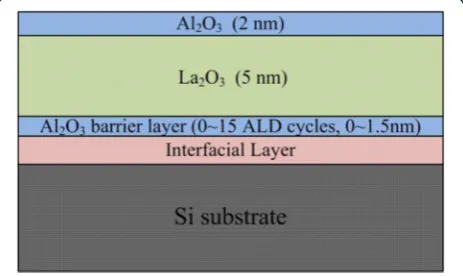
Figure 1 shows the schematic structure of Al2O3/La2O3/
Al2O3gate stacks discussed in this paper. The thickness
of La2O3layers in samples S1 ~ S4 is 5 nm, and all the
samples are in situ ALD-capped with a 2-nm Al2O3
layer. The thickness of the Al2O3 barrier layer between
La2O3 layers and Si substrate is tuned by varying the
number of ALD cycles, which is 0, 5, 10, and 15 cycles for samples S1 ~ S4 separately. Table 1 shows the total thickness of the as-grown and annealed samples mea-sured by spectroscopic ellipsometry (SE). It is reported that La2O3 films are easily hydrated, but in this work,
the existence of capping Al2O3layer suppresses the
hy-dration reaction during the rapid thermal annealing (RTA) process, and as a result, the thickness of each sample does not increase too much after the annealing treatment. However, sample S1 shows a thicker incre-ment about 0.4 nm when compared with the other three samples, which indicates a thicker interfacial layer for-mation in sample S1.
Figure 2 shows the O 1s XPS spectra and their decon-volution results for the RTA treated Al2O3/La2O3/Al2O3
[image:2.595.306.538.558.696.2]gate stacks. C 1s peak from adventitious carbon at 284.6 eV [13] was used as an internal energy reference during the analysis. The O 1s XPS spectra consists of
Figure 1Schematic structure of Al2O3/La2O3/Al2O3/Si stacks.
The thickness of Al2O3barrier layer between Si substrate and La2O3
four peaks, which are (I) La-O-La (approximately 529.3 eV), (II) La-O-Si (approximately 530.4 eV), (III) Al-O (approximately 531.6 eV), and (IV) Si-O-Si (approximately 532.6 eV) [14]. Among the four deconvo-luted peaks, peak I and peak III come from the depos-ited La2O3 and Al2O3 layer; peak II and peak IV are
attributed to SiOxand La-silicate, which indicate the
for-mation of interfacial layer and silicate in the films caused by the diffusion of oxygen and Si atoms during the an-nealing process [15]. By contrast, we can find out that the intensity of peak II and peak IV corresponding to
La-O-Si and Si-O-Si is reduced from samples S1 to S4, respectively. The decreasing trend of peak II and peak IV suggests that, on the one hand, in sample S1 without an Al2O3barrier layer, Si diffusion into the La2O3 layer
is enhanced during a thermal treatment, resulting in a favorable silicate formation through the film and the interface; on the other hand, to some extent, a uniform and dense Al2O3barrier layer (approximately 1.5 nm) in
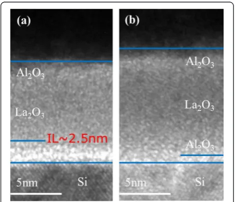
sample S4 produced by 15 cycles of ALD deposition suppresses the formation of IL and prevents the diffu-sion of Si atoms, resulting in a silicate formation de-crease. In order to study this phenomenon more clearly, cross-sectional HRTEM and time of flight secondary ion mass spectrometry (TOF-SIMS) measurements were applied to samples S1 and S4.
With the deposition method of ALD, different from the LaLuO3/Si stack, in which a sharp interface is
ob-served [16], the IL seems hardly to be avoided in the La2O3/Si stack because of the affinity for silicon atoms
of La2O3, especially after a high-temperature RTA
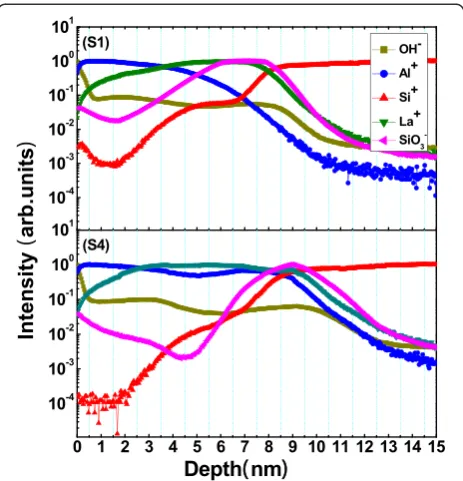
treat-ment. The cross-sectional HRTEM images for annealed samples S1 and S4 are displayed in Figure 3. Both of the films exhibit an amorphous structure up to an annealing temperature of 700°C [17]. Compared with Figure 3b, a thicker amorphous transition region about 2.5 nm be-tween the deposited film and Si substrate is observed in Figure 3a, indicating a thicker IL formation in sample S1. Figure 4 shows the TOF-SIMS depth profiles of OH−, Al+, Si+, La+, and SiO3− clusters acquired for
[image:3.595.56.291.112.190.2]samples S1 and S4. The intensity of the signals is dealt with normalization method, and depth values are cali-brated by HRTEM results. Large amounts of OH−are de-tected only at the surface of the films while the internal
Table 1 Thickness (measured by SE) of the as-grown and annealed samples discussed in this work
Sample Number of ALD Al2O3cycles
Thickness as-grown (nm)
Thickness after RTA (nm)
S1 0 8.2 8.6
S2 5 8.4 8.7
S3 10 8.8 9.0
[image:3.595.57.290.366.706.2]S4 15 9.3 9.5
Figure 2O 1s XPS spectra of Al2O3/La2O3/Al2O3gate stacks shown in Table 1.
[image:3.595.304.541.503.705.2]content is much less and uniformly distributed without a gradient distribution trend suggesting that the diffusion of moisture from air to the films is suppressed by the capping Al2O3layer. As a result, the moisture absorption
of La2O3 layer can be neglected in the Al2O3/La2O3/
Al2O3gate stacks [7]. The intensity of Si+in sample S4 is
at least an order magnitude less than that in sample S1, which suggests that the deposited Al2O3 barrier layer
(15 cycles) in sample S4 indeed suppresses the diffusion of Si atoms from the Si substrate into the La2O3 layer
during the thermal process, in good agreement with the XPS results. Due to the formation of pinholes in the Al2O3barrier layer during the 700°C RTA treatment [18],
the diffusion of Si atoms is not completely suppressed. HRTEM analysis reveals the existence of a thicker IL in the sample without an Al2O3barrier layer, and now this
result can be further confirmed from the intensity of SiO3− signals which indicate the presence of a SiOx-like
component existing in the region of the nanolaminate/ substrate interface. Finally, the depth profiles of Al+and La+ suggest a serious interdiffusion of La2O3and Al2O3
layers in the Al2O3/La2O3/Al2O3gate stacks. This result
explains the difficulty in distinguishing the borderlines between La2O3and Al2O3layers in Figure 3.
Figure 5 shows the C-Vcurves and VFB shifts for the Al2O3/La2O3/Al2O3 gate stacks. The EOTs of samples
S1 ~ S4 extracted by NCSU CVC program are 4.62, 3.82, 3.85, and 3.28 nm, then the kvalues can be figured out as 7.3, 8.9, 9.1, and 11.3, respectively. For sample S1, the enhanced diffusion of oxygen and Si atoms during the
annealing process owing to the absence of Al2O3barrier
[image:4.595.58.290.88.329.2]layer makes the permittivity lower while the EOT thicker with respect to those of the others. The doping con-centration of the Si substrate used in this work is 5.0 × 1015 cm−3, considering the work function differ-ence between Si substrate and Au/Ni metal gate elec-trode, the ideal VFB can be worked out as−0.06 V. It is believed that the shift of VFB originates from the exist-ence of net oxide charges in the films [19]. TheVFBvalue for sample S1 is−0.16 V. Accordingly, there are positive net oxide charges in sample S1. The VFB value for sam-ples S2 ~ S4 are observed to be 0.05, 0.15, and 0.26 V, respectively. Such VFB shifts suggest the presence of negative net oxide charges induced by the negative fixed charges existing in the Al2O3barrier layers [20]. Taking
[image:4.595.306.539.88.269.2]Figure 4TOF-SIMS depth profiles of annealed samples S1 and S4 shown in Table 1.
[image:4.595.305.540.529.705.2]Figure 5C-Vcurves of MIS capacitors using annealed S1 ~ S4 gate stacks as insulators.The capacitors were measured at the frequency of 1 MHz.
the idealVFBas a reference, a bigger shifting value ofVFB is obtained in sample S4 compared with those of sample S2 and sample S3, which means that, in a very thin range, more negative net oxide charges in the Al2O3/La2O3/
Al2O3gate stacks would be generated as the thickness of
Al2O3barrier layer increases.
The effect of Al2O3barrier layer thickness on the gate
leakage current density is shown in Figure 6. At the ap-plied gate voltage of−5 V, the leakage current density of the films are measured to be 5.92 × 10⁻¹, 1.86 × 10⁻³, 2.32 × 10⁻⁴, and 1.79 × 10⁻⁴ A/cm2, separately. The current density reduction of sample S4 by three orders or more from sample S1 is achieved. The low gate leakage current characteristic of sample S4 is consid-ered arise from the large band offsets [21] at the nanolaminate/Si interface. Al2O3 has a large band
gap of 8.8 eV and high values of conduction band offset (approximately 2.8 eV) and valence band offset (approximately 4.8 eV) with respect to p-type Si sub-strate [22,23]. Consequently, the addition of an Al2O3
barrier layer contributes to the formation of a higher potential barrier at the fabricated nanolaminate/Si interface than that at the La2O3/Si interface or the
SiOx-silicate/Si interface. The high potential barrier
formed between the oxide film and the Si substrate re-sults in a weakening of the tunneling effect of elec-trons and holes in the metal-insulator-semiconductor capacitor. Therefore, the leakage current density de-creases with the existence of an Al2O3barrier layer. Conclusions
In summary, an Al2O3barrier layer (15 ALD cycles,
ap-proximately 1.5 nm) between the La2O3layer and Si
sub-strate plays an important role in blocking the diffusion of Si atoms from Si substrate into the La2O3layer and the
dif-fusion of oxygen in the opposite direction resulting in a decrease in the thickness of IL and the formation of La-silicate in the Al2O3/La2O3/Al2O3gate stack during the
an-nealing process. In other words, the existence of the Al2O3
barrier layer provides a gate stack with high permittivity and contributes to the achievement of an improved EOT value. The thickness of the Al2O3barrier layer also affects
the electrical characteristics of the fabricated nanolami-nates. In a very thin range (0 ~ 15 cycles), Al2O3 barrier
layer brings in negative net oxide charges which leads to a positive shift ofVFB. In addition, as the thickness of Al2O3
barrier layer increases, gate leakage current is reduced due to the formation of a high potential barrier between the oxide film and Si substrate.
Abbreviations
ALD:atomic layer deposition; CMOS: complementary metal oxide semiconductor; EOT: equivalent oxide thickness; HRTEM: high resolution transmission electron microscopy; IL: interfacial layer; MIS: metal-insulator-semiconductor; MOSFET: metal-oxide-semiconductor field-effect transistor;
RTA: rapid thermal annealing; SE: spectroscopic ellipsometry; TOF-SIMS: time of flight secondary ion mass spectrometry; XPS: X-ray photoelectron spectroscopy.
Competing interests
The authors declare that they have no competing interests.
Authors’contributions
XW generated the research idea, analyzed the data, and wrote the paper. XW and CxF carried out the experiments and the measurements. SyY and XjF participated in the discussions. HxL has given final approval of the version to be published. All authors read and approved the final manuscript.
Acknowledgements
This research is supported by the National Natural Science Foundation of China (grant no. 61376099 and 11235008) and the Specialized Research Fund for the Doctoral Program of Higher Education (grant no. 20130203130002 and 20110203110012).
Received: 16 November 2014 Accepted: 27 February 2015
References
1. Lee BH, Oh J, Tseng HH, Jammy R, Huff H. Gate stack technology for nanoscale devices. Mater Today. 2006;9(6):32–40.
2. Saito S, Torii K, Shimamoto Y, Tonomura O, Hisamoto D, Onai T. Remote-charge-scattering limited mobility in field-effect transistors with SiO2and
Al2O3/SiO2gate stacks. J Appl Phys. 2005;98:113706.
3. Kawanago T, Suzuki T, Lee Y, Kakushima K, Ahmet P, Tsutsui K, et al. Compensation of oxygen defects in La-silicate gate dielectrics for improving effective mobility in high-k/metal gate MOSFET using oxygen annealing process. Solid-State Electron. 2012;68:68–72.
4. Kouda M, Suzuki T, Kakushima K, Ahmet P, Iwai H, Yasuda T. Electrical properties of CeO2/La2O3stacked gate dielectrics fabricated by chemical
vapor deposition and atomic layer deposition. Jpn J Appl Phys. 2012;51:121101.
5. Kim WH, Maeng WJ, Moon KJ, Myoung JM, Kim H. Growth characteristics and electrical properties of La2O3gate oxides grown by thermal and
plasma-enhanced atomic layer deposition. Thin Solid Films. 2010;519:362–6. 6. Fanciulli M, Scarel G. Rare earth oxide thin film: growth, characterization and
applications. Top Appl Phys. 2007;106:1–14.
7. Lamagna L, Wiemer C, Perego M, Volkos SN, Baldovino S, Tsoutsou D, et al. O3-based atomic layer deposition of hexagonal La2O3films on Si(100) and
Ge(100) substrates. J Appl Phys. 2010;108:084108.
8. Liu KC, Tzeng WH, Chang KM, Huang JJ, Lee YJ, Yeh PH, et al. Investigation of the effect of different oxygen partial pressure to LaAlO3thin film
properties and resistive switching characteristics. Thin Solid Films. 2011;520:1246–50.
9. Suzuki M, Nishi Y, Kinoshita A. Gate-first metal-gate/high-kn-MOSFETs with deep sub-nm equivalent oxide thickness (0.58 nm) fabricated with sulfur-implanted schottky source/drain using a low-temperature process. IEEE Trans Electron Dev. 2011;58(11):3674–7.
10. Wiemer C, Lamagna L, Fanciulli M. Atomic layer deposition of rare-earth-based binary and ternary oxides for microelectronic applications. Semicond Sci Technol. 2012;27:074013.
11. Schamm S, Coulon PE, Miao S, Vollkos SN, Lu LH, Lamagna L, et al. Chemical/structural nanocharacterization and electrical properties of ALD-grown La2O3/Si interfaces for advanced gate stacks. J Electrochem
Soc. 2009;156:H1–6.
12. Hauser J. NCSU CVC software, version 7.0. Raleigh, USA: Department of Electrical and Computer Engineering, North Carolina State University. 13. Pelloquin S, Saint-Girons G, Baboux N, Albertini D, Hourani W, Penuelas J,
et al. LaAlO3/Si capacitors: comparison of different molecular beam
deposition conditions and their impact on electrical properties. J Appl Phys. 2013;113:034106.
14. Lee B, Park TJ, Hande A, Kim MJ, Wallace RM, Kim J, et al. Electrical properties of atomic-layer-deposited La2O3films using a novel La formamidinate precursor
and ozone. Microelectron Eng. 2009;86:1658–61.
diffusion behavior in atomic-layer-deposited La2O3thin films. Appl Surf Sci.
2014;292:880–5.
16. Shen S, Liu Y, Gordon RG, Brillson LJ. Impact of ultrathin Al2O3diffusion
barriers on defects in high-kLaLuO3on Si. Appl Phys Lett. 2011;98:172902.
17. Eom D, No SY, Park H, Hwang CS, Kim HJ. Improvement in thermal stability of stacked structures of aluminum nitride and lanthanum oxide thin films on Si substrate. Electrochem Solid-State Lett. 2007;10:G93–6.
18. Lee WJ, Ma JW, Bae JM, Kim CY, Jeong KS, Cho MH, et al. The diffusion of silicon atoms in stack structures of La2O3and Al2O3. Curr Appl Phys.
2013;13:633–9.
19. Kim H, Woo S, Lee J, Kim H, Kim Y, Lee H, et al. The effects of annealing ambient on the characteristics of La2O3films deposited by RPALD.
J Electrochem Soc. 2010;157:H479–82.
20. Kornblum L, Meyler B, Cytermann C, Yofis S, Salzman J, Eizenberg M. Investigation of the band offsets caused by thin Al2O3layers in HfO2based
Si metal oxide semiconductor devices. Appl Phys Lett. 2012;100:062907. 21. Suzuki M. Comprehensive study of lanthanum aluminate
high-dielectric-constant gate oxides for advanced CMOS devices. Materials. 2012;5:443–77. 22. Mönch W. On the band structure lineup at interfaces of SiO2, Si3N4, and
high-k dielectrics. Appl Phys Lett. 2005;86:122101.
23. Liu D, Clark SJ, Robertson J. Oxygen vacancy levels and electron transport in Al2O3. Appl Phys Lett. 2010;96:032905.
Submit your manuscript to a
journal and benefi t from:
7Convenient online submission
7Rigorous peer review
7Immediate publication on acceptance
7Open access: articles freely available online
7High visibility within the fi eld
7Retaining the copyright to your article