PS2-VGA Peripheral based Character Display using
FPGA
B. Murali Krishna
Assistant professor
Dept of ECE
K L University
V. G. Santhi Swaroop
M.Tech, student
Dept of ECE
K L University
K. Gnana Deepika
M.Tech, student
Dept of ECE
K L University
Habibullah Khan, PhD.
Professor
Dept of ECE
K L University.
ABSTRACT
The aim of this paper is to print characters by providing the interfaces to connect a VGA port for graphical output and a PS/2 port for keyboard input. This system is then to be synthesized on an FPGA board, and should be capable of running a program to display characters that takes input from the keyboard and prints the results to a VGA monitor.
This paper is developed under the environment of Xilinx ISE and Platform Studio. It includes Xilinx provided hardware, VHDL IP core and MICROBLAZE processor, the characters inputted by ps2 keyboard, and will be displayed on the VGA monitor. Based on Spartan 3E Starter Board Hardware Architecture, Software Development mainly consists of two parts: one is that PS/2 keyboard scan code receiving and processing program, the other one is VGA displaying program.
Keywords: Xilinx platform studio, Xilinx-c, IP core, MICROBLAZE processor
1.
INTRODUCTION
Embedded Development Kit (EDK) is a suite of tools and Intellectual Property (IP) that enables you to design a complete embedded processor system for implementation in a Xilinx Field Programmable Gate Array (FPGA) device. Xilinx Platform Studio (XPS) is the development environment used for designing the hardware portion of your embedded processor system using MICROBLAZE processor.
The MICROBLAZE has a versatile interconnect system to support a variety of embedded applications. MICROBLAZE'S primary I/O bus, the Core Connect PLB bus, is a traditional system-memory mapped transaction bus with master/slave capability
.
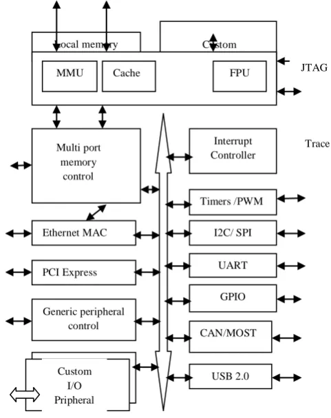
The MICROBLAZE processor is a 32-bit Harvard Reduced Instruction Set Computer (RISC architecture optimized for implementation in Xilinx FPGAs with separate 32-bit instruction and data buses running at full speed to execute programs and access data from both on-chip and external memory at the same time. The backbone of the architecture is a single-issue, 3-stage pipeline with 32 general-purpose register, an Arithmetic Logic Unit (ALU), a shift unit, and two levels of interrupt. This basic design can then be configured with more advanced features to tailor to the exact needs of the target embedded application such as: barrel shifter, divider, multiplier, single precision floating-point unit (FPU), instruction and data caches, exception handling, debug logic, Fast Simplex Link (FSL) interfaces and others. Thisflexibility allows the user to balance the required performance of the target application against the logic area cost of the soft processor. Figure 1 shows a view of a MICROBLAZE system. The items in white are the backbone of the MICROBLAZE architecture while the items shaded gray are optional features available depending on the exact needs of the target embedded application. Because MICROBLAZE is a soft-core microprocessor, any optional features not used will not be implemented and will not take up any of the FPGAs resources.
[image:1.595.310.551.361.665.2]
Fig 1. MicroBlaze Processor System Architecture
Writing software to control the MicroBlaze processor must be done in C/C++ language. Using C/C++ is the preferred method by most people and is the format that the Xilinx Embedded Development Kit (EDK) software tools expect. The EDK tools have built in C/C++ compilers to generate the necessary machine code for the MicroBlaze processor.
Local memory Custom
Coprocessor
MMU Cache FPU
The MICROBLAZE processor is useless by itself without some type of peripheral devices to connect to and EDK comes with a large number of commonly used peripherals. Here we are using PS2 and VGA peripherals to develop the application in EDK-XPS using MICROBLAZE processor in SPARTAN 3E starter board
.
2.
PS2 PRIPHERAL
The Spartan-3E FPGA Starter Kit board includes a PS/2 mouse/keyboard port and the standard 6-pin mini-DIN connector, labeled J14 on the board. Only pins 1 and 5 of the connector attach to the FPGA.
Fig 2 . PS2 connector
Both a PC mouse and keyboard use the two-wire PS/2 serial bus to communicate with a host device, the Spartan-3E FPGA in this case. The PS/2 bus includes both clock and data. Both a mouse and keyboard drive the bus with identical signal timings and both use 11-bit words that include a start, stop and odd parity bit. However, the data packets are organized differently for a mouse and keyboard. Furthermore, the keyboard interface allows bidirectional data transfers so the host device can illuminate state LEDs on the keyboard.
Ps/2 DIN Pin Signal FPGA Pin
1 Data (PS2_DATA) G13
2 Reserved G13
3 GND GND
4 +5v --
5 CLK G14
6 Reserved G13
Fig 3. PS2 connector pinout
The keyboard uses open-collector drivers so that either the keyboard or the host can drive the two-wire bus. If the host never sends data to the keyboard, then the host can use simple input pins. A PS/2-style keyboard uses scan codes to communicate key press data. Nearly all keyboards in use today are PS/2 style. Each key has a single, unique scan code that is sent whenever the corresponding key is pressed.If the key is pressed and held, the keyboard repeatedly sends the scan code every 100 ms or so. When a key is released, the keyboard sends an “F0” key-up code, followed by the scan code of the released key. The keyboard sends the same scan code, regardless if a key has different shift and non-shift characters and regardless whether the Shift key is pressed or not. The host determines which character is intended.
Some keys, called extended keys, send an “E0” ahead of the scan code and furthermore, they might send more than one scan code. When an extended key is released, an “E0 F0” key-up code is sent, followed by the scan code. The keyboard sends commands or data to the host only when both the data and clock lines are High, the Idle state.Because the host is the bus master, the keyboard checks whether the host is sending
data before driving the bus. The clock line can be used as a clear to send signal. If the host pulls the clock line Low, the keyboard must not send any data until the clock is released.
3.
VGA PERIPHERAL
The Spartan 3E FPGA Starter Kit board includes a VGA display port via a DB15 connector. Connect this port directly to most PC monitors or flat-panel LCDs using a standard monitor cable. The below figure shows VGA connector.
Fig 4. VGA connector
The Spartan-3E FPGA directly drives the five VGA signals via resistors. Each color line has a series resistor, with one bit each for VGA_RED, VGA_GREEN, and VGA_BLUE. The VGA_HSYNC and VGA_VSYNC signals using LVTTL or LVCMOS33 I/O standard drive levels.
Drive the VGA_RED, VGA_GREEN, and VGA_BLUE signals High or Low to generate the eight colors shown below
VGA_RED VGA_GREEN VGA_BLUE RESULTING
COLOUR
0 0 0 black
0 0 1 blue
0 1 0 green
0 1 1 cyan
1 0 0 red
1 0 1 magenta
1 1 0 yellow
1 1 1 white
Fig 5. 3 bit binary color codes
4.
IMPLEMENTATION
4.1
PS2-VGA initialization using XPS
XPS-PS2 is the IP core that is provided by XILINX plat form studio after creating a sample project. Xps_ps2 is added by selecting IP catalog tab in project information tab in XPS. The selected IP core will appear in bus interface tab of system assembly view. The ps2 controller will be connected to mb_plb i.e. the processor local bus connection in order to perform communication with MICROBLAZE processor.
Fig6. IP core creation for PS2 & VGA peripherals
4.2
Making PS2-VGA ports externals
After the initialization of PS2-VGA IP cores the respective ports must be made external. After making the external the ports of the peripherals connected to the MICROBLAZE processer local bus.
Fig7 . PS2-VGA ports are made external
4.3 Adress generation
After making the ports externals of these two peripherals the adress will generate at adress tab in system assemly view. It gives the base adress and high adress for thse both PS2 and VGA peripherals.
After the adress genaration MHS(Microprocessor hardware specification) and MPD(Microprocessor peripheral descripton ) must be edit depends upon peripheral device configuration. The UCF(user constraint file) must be given at the system.ucf in project information tab.
Fig8 . Adress generated for PS2-VGA peripherals
5.
EXPERIMENTAL SETUP
The total experiment is done by using spartan 3e starter kit ( XC3S500E-Device family,FG 320 package and 4-speed grade). The interface between PS2 and VGA is done by using Xilinx Platform Studio.The total application is developed by writing required logic in Embedded-C.
Fig9. Experimental setup
PS2 Keyboard VGA
SPARTAN 3E
6.
EXPERIMENTAL RESULTS
[image:4.595.57.271.348.747.2]Fig10 .Hardware setup for PS2-VGA Peripherals
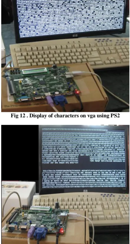
Fig 12 . Display of characters on vga using PS2
Fig13 . Deteting the characters using backspace key
Fig14 . Display of characters using RGB colours
Fig15 . Design summery
Fig16 . Device utilization summary
7.
CONCLUSION
8.
REFERENCES
[1] “EDK Concepts, Tools, and Techniques” by Xilinx Corporation.
[2] “EDK MICROBLAZE Tutorial” by Xilinx Corporation.
[3] Spartan-3E FPGA Starter Kit Board User Guide http://www.xilinx.com/support/documentation/boards_an d_kits/ug230.pdf
[4] “Create or Import Peripheral wizard on EDK” by Xilinx Corporation.
[5] Wikipedia http://en.wikipedia.org/wiki/Fpga.
[6] www.computerengineering.org/ps2keyboard/scancodes2
[7] “A Control Design Approach for Controlling an Autonomous Vehicle with FPGAs” JOURNAL OF COMPUTERS, VOL. 5, NO. 3, MARCH 2010.
[8] “Soft core processors and Embedded processing : a survey and analysis” by Humberto Calderón, Christian Elena and Stamatis Vassiliadis.
[9] “Experiences with Soft-Core Processor Design” Proceedings of the 19th IEEE International Parallel and Distributed Processing Symposium.