Available Online at www.ijpret.com 128
INTERNATIONAL JOURNAL OF PURE AND
APPLIED RESEARCH IN ENGINEERING AND
TECHNOLOGY
A PATH FOR HORIZING YOUR INNOVATIVE WORK
LOW POWER DIGITAL PULSE CONTROLLER USING FOOTER METHOD
M. VIVEK KUMAR1, S. RATHIMEENA2, S. SARMILA2, ANILA RAMACHANDRAN2 1.Assistant Professor, ECE dept, Sri Eshwar College of Engineering, Coimbatore.
2.ME VLSI Design, Sri Eshwar College of Engineering, Coimbatore
Accepted Date: 26/02/2015; Published Date: 01/03/2015
\
Abstract: A digitally controlled pulse width modulator (PWM) targeting on-chip power management applications is proposed in this paper. A current starved ring oscillator, with digitally controlled current source based headers and footers, is used to provide a versatile duty cycle and an accurate frequency control. The proposed circuit achieves i) a controlled duty cycle that can vary between 20% and 90% and ii) a compensation circuit that guarantees a constant duty cycle under process, voltage, and temperature (PVT) variations. A fast response time of 5 ns – 20ns with a fine duty cycle granularity has been achieved through the proposed control techniques. The circuit operates at a frequency range of 500 MHz – 1.66 GHz and is implemented with a 22 nm CMOS predictive technology model.
Keywords: Current starvation, digital-controlled oscillators, pulse width modulation, ring oscillators.
Corresponding Author: MS. S. RATHIMEENA
Access Online On:
www.ijpret.com
How to Cite This Article:
S. Rathimeena, IJPRET, 2015; Volume 3 (7): 128-137
Available Online at www.ijpret.com 129 INTRODUCTION
A pulse width modulator (PWM) is used to generate a periodic switching signal with a varying duty cycle and can be configured to control the duty of a switching signal. Various architectures have been proposed to generate pulse width modulated signals. A voltage controlled oscillator, a counter, a digital to analog converter, and a comparator are used as the building blocks of a PWM [1].
This counter based PWM requires additional clock and reference signals and therefore suffers from large power consumption. PWMs based on either a delay line multiplexor and a ring oscillator multiplexor are described, respectively, in [2] and [3] which consume less power but occupy a large chip area due to the large multiplexor circuits. PWMs based on a delay line multiplexor and a ring oscillator counter provides a means to control area/power tradeoffs [4]. A small and power efficient on-chip PWM requires a small and power efficient oscillator.
A modified ring oscillator circuit is proposed to satisfy these requirements within the PWM. Voltage controlled oscillators (VCOs) are widely used to generate a switching signal where certain characteristics of this signal can also be controlled. Two types of VCOs are primarily used in high performance integrated circuits (ICs); inductor-capacitor (LC) oscillators and ring oscillators. LC oscillators can operate at high frequencies and exhibit superior noise performance.
Fig1.conventional ring oscillator circuit
A conventional ring oscillator circuit is shown in Fig. 1. Duty cycle and frequency control are achieved by controlling the supply current of individual inverter stages [5]-[6]. Changing the supply current of individual inverter stages within a ring oscillator affects the transition delay characteristics of the corresponding stages, resulting in an output with a variable duty cycle. PVT variations affect the delay characteristics of the stages resulting in duty cycle variations.
Available Online at www.ijpret.com 130
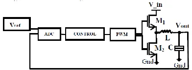
circuits can be added to provide robust duty cycle under PVT variations over a wide frequency range [5]-[6]. This principle has been used in the proposed PWM circuit. Utilizing a ring oscillator as a PVT-stable frequency source has been described in [10]-[13]. PVT compensations in these designs are either based on a band gap reference (BGR) or a sophisticated proportional to absolute temperature (PTAT) circuit that requires additional chip area. An application of PWM is shown in Fig. 2 for an inductive switching DC-DC voltage converter [8]-[9]. This circuit senses the DC-DC converter analog output (Vout) and converts this voltage to a digital signal with the analog to digital converter (ADC) block.
The digital signal is processed with control algorithm (CONTROL) that converts the signal into a pulse width modulated form. The pulse width modulated signal from (PWM) block is applied to pass transistors (M1,M2), providing a stable load current. LC filter provides a stable output voltage (Vout).The duty cycle of the generated switching signal is typically 50% for conventional ring oscillators where the PMOS and NMOS transistors within the inverters provide the same rise and fall transition times. These circuits have been typically implemented off-chip
This work focuses on an adaptive PWM circuit that can be fully integrated on chip. The proposed PWM architecture and working principles of the ring oscillator, header, and footer control circuits are described in Section II. Simulation results and comparisons with analytic expressions are presented in Section III. Circuit comparisons and result are presented in section IV
Fig. 2. Typical DC-DC inductance based switching regulator.
II. PULSE WIDTH MODULATOR ARCHITECTURE
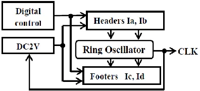
An architectural level block diagram of the proposed PWM based on a ring oscillator is shown in Fig. 3. DC2V provides an analog control signal for the headers and footers to ensure a stable duty cycle under PVT variations. Digital control provides signals for the header and footer circuits to dynamically change the duty cycle and frequency of the ring oscillator.
Available Online at www.ijpret.com 131
B. PWM Control
C. Duty Cycle to Voltage Converter
D. Header and Footer Circuits.
A. Ring Oscillator Topology
A seven stage ring oscillator [5]-[6] is used for the proposed PWM as shown in Fig. 4. The odd inverter stages 1, 3, 5, and 7 are connected to header circuit Ia and footer circuit Ic. The even inverter stages 2, 4, and 6 are connected to header circuit Ib and footer circuit Id.
Fig. 3. Block diagram of the proposed pulse width modulator.
Conversely, an increase of the sink current through the footer Ic or Id increases the current through the NMOS devices of the inverters, enhancing the pull down capability and resulting in a faster fall time at the output. The gate voltage of these switch transistors is controlled by a digital controller to turn on and off the individual header stages. Turning on the entire header stages passes the maximum current to the ring oscillator which minimizes the duty cycle.
B. PWM Control
Available Online at www.ijpret.com 132 Fig.4. Seven stage ring oscillator circuit topology
Where D is the duty cycle of proposed PWM, and Fnew is the new frequency of the PWM.
C. Duty Cycle to Voltage Converter
The duty cycle to voltage converter (DC2V) has been adopted from [14]. A simplified diagram of the circuit is shown in Fig. 5 and has the following cycles of operation. A high CLK input charges capacitor C1 from Vdd through transistor DM0.
Fig.5. Simplified schematic of DC2V.
Available Online at www.ijpret.com 133 III. PROPOSED FOOTER CIRCIIT
The circuit schematics for headers Ia, Ib, and footers Ic, Id are shown in Figs. 6 and 9, respectively. Addition based current sources and sinks are proposed in [6] to ensure stable and robust current delivery under PVT variations.
A modified addition based current source has been used within the header circuit using PMOS transistors PM0, PM2, PM3, and PM4. PMOS transistors PM5, PM6, and PM7 in series with PM2, PM3, and PM4 respectively control the header currents with digital inputs bx0, bx1… bxn.
A modified addition based current sink has been used within the footer circuit using NMOS transistors NM1, NM3, NM4, and NM5. NMOS transistors NM6, NM7 and NM8 in series with NM3, NM4, and NM5, respectively, control the footer currents with digital input by0, by1… byn.
Fig 6. Footer circuit Ic or Id. Digital inputs by0, by1.. byn control total footer current sinking through output port Outn.
The analog input dc2vin received from output of DC2V block provides current control for the header and footer circuits to maintain a constant current over a wide range of PVT variations.
Under PVT variations, the bias voltage for transistors PM2, PM3, and PM4 in the header circuit and transistors NM3, NM4, and NM5 in the footer circuits respectively are adjusted to maintain current values that ensure a constant duty cycle for the PWM. Device PM00 and resistor RN1 within the footer circuits provide a level shift circuit for dc2vin.
Available Online at www.ijpret.com 134
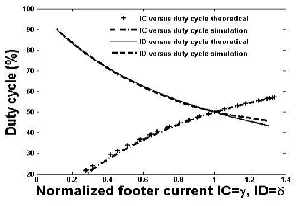
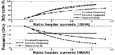
The ratio of the header currents IB to IA is changed to achieve a constant frequency of 1.66 GHz, over a wide range of duty cycles. Header current ratio IB/IA versus duty cycle and frequency with and without frequency compensation are shown in Fig. 8.
Fig. 8. Constant frequency simulation and theoretical comparison.
Table-1 Duty Cycle and frequency changes with header and footer currents
Fig 9.. Footer circuit Ic or Id.
Digital inputs by0, by1.. byn control total footer current sinking through output port Outn.
IV. SIMULATION RESULTS
Available Online at www.ijpret.com 135 Fig.10. combined heater and footer circuit
Fig.10.1 combined heater and footer output waveform
Fig. 10. 2 power calculation table in header and footer circuit
Available Online at www.ijpret.com 136 Table ii -PROCESS (P) SS= slow, FF= Fast, TT=Typical,VOLTAGE (V) = 0.9V – 1V, TEMP (T) = 27 °C
- 80 °C
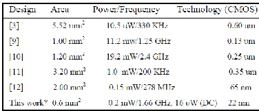
A comparison of the proposed PWM with state-of-the-art PWMs is provided in Table III. The proposed PWM can be implemented in a small area and consumes significantly less power over a wide frequency range.
Table iii -AREA, POWER AND FREQUENCY OF OPERATION COMPARED
V. CONCLUSIONS
A digitally controlled PWM has been proposed that adaptively changes the header and footer current profiles to maintain a constant duty cycle under PVT variations. The proposed circuit can adaptively control the duty cycle and the frequency at runtime. A DC2V converter and novel header and footer circuits are employed to achieve a stable duty cycle operation under PVT variation.
REFERENCES
1. G. Wei and M. Horowitz, “A Low Power Switching Power Supply for Self-Clocked Systems,” Proceedings of the International Symposium on Low Power Electronics and Design, pp. 313-317, August 1996.
Available Online at www.ijpret.com 137
3. A. P. Dancy and A. P. Chandrakasan, “Ultra Low Power Control Circuits for PWM Converters,” Proceedings of the Power Electronics Specialists Conference, Vol. 1, pp. 21-27, June 1997.
4. A. P. Dancy, R. Amirtharajah, and A. P. Chandrakasan, “High- Efficiency Multiple Output DC-DC Conversion for Low-Voltage Systems,” IEEE Transaction on VLSI Systems, Vol. 8, No. 3, pp. 252-263, June 2000.
5. S. Köse, I. Vaisband, and E. G. Friedman “Digitally Controlled Wide Range Pulse Width Modulator for On-Chip Power Supplies,” Proceedings of the IEEE International Symposium on Circuits and Systems, pp. 2251-2254, May 2013.
6. R. Jakushokas, M. Popovich, A. V. Mezhiba, S. Köse, and E. G. Friedman, Power Distribution Networks with On-Chip Decoupling Capacitors, 2nd ed. New York: Springer-Verlag, 2011.
7. S. Köse, S. Tam, S. Pinzon, B. McDermott, and E. G. Friedman, "Active Filter-Based Hybrid On-Chip DC–DC Converter for Point-of-Load Voltage Regulation", IEEE Transactions on VLSI Systems, Vol. 21, No. 4, April 2013
8. K. R. Lakshmikumar, V. Mukundagiri, and S. L. J. Gierkink, “A Process and Temperature Compensated Two Stage Ring Oscillator,” Proceedings of the IEEE Custom Integrated Circuits Conference, pp.691-694, September 2007.
9. V. Cheynet et al., “Cmos 2.45 GHz Ring Oscillator with Temperature Compensation,” Proceedings of the IEEE International Conference on Electronics, Circuits and Systems, pp. 1-4, December 2005.
10.J. Nebhen et al., “A Temperature Compensated CMOS Ring Oscillator For Chopper Amplifier MEMS Gas Sensor,” Proceedings of the IEEE Conference on Ph.D. Research in Microelectronics and Electronics (PRIME), pp. 1-4, June 2012.
11.C. Chang, S. Jou, and Y. Chu, “0.5 VDD Digitally Controlled Oscillators Design with Compensation Techniques for PVT Variations,’’ Proceedings of the IEEE International Conference on ASIC, pp. 606-609, October 2011.