[Gomez* 5(12): December, 2018] ISSN 2349-4506
Impact Factor: 3.799
G
lobal
J
ournal of
E
ngineering
S
cience and
R
esearch
M
anagement
ASSEMBLY AND TEST PROCESS OPTIMIZATION FOR SCALABLE PACKAGE
SEMICONDUCTOR DEVICE
Antonio R. Sumagpang Jr., Frederick Ray I. Gomez
*
Back-End Manufacturing & Technology, STMicroelectronics, Inc.
9 Mountain Drive, Light Industry & Science Park II, Brgy. La Mesa, Calamba City, Laguna, Philippines
4027
DOI: 10.5281/zenodo.2264935
KEYWORDS
:
Semiconductor; assembly scalable package; line stressing; design of experiments.ABSTRACT
The technical paper presents a methodological approach to deal with a new product trend that will be successfully manufactured during assembly production ramp-up. The project is intended to determine the required process flow and machine platforms for high-density and high-complexity scalable device. Critical processes are shown and top reject contributors are addressed through systematic method by using statistical tools and in-depth engineering analysis.
The Scalable Package Semiconductor Device is one of the newest and latest developed device in the plant, which functions as a diode for mobile and computer applications. The device is considered high density as its 6” single wafer is equivalent to 400,000 units compared to conventional device consisting of only 1,000 units. In addition, it is considered as a device with high complexity as state-of-the-art platforms are needed to satisfy its output process. Furthermore, the device has a very thin die and with the smallest total package dimension. The process of assembly manufacturing includes a step cutting method of wafers, compression molding, and in-strip testing, which are unlikely to be found on other semiconductor industries. Ultimately, complex errors and top reject contributor of identified critical processes are corrected and the target or required process capability index is effectively achieved.
INTRODUCTION
In order to cope with the fast-paced technology in semiconductor industry, one should have a very good impression from the customer be it internal or external. This is one of the biggest challenges for any semiconductor company in order to maintain its competitive market position and value. However, failure to provide customer expectation in terms of on-time delivery will result to possible business failure. This critical scenario should be avoided that’s why a risk production or line stressing is being done in preparation to full production mode. A total of 10 to 30 lots are line stressed to capture all hindrances in the production line and thus corrected immediately to prevent delivery issues.
Delinquency in view of customer or missed deliveries was the scenario encountered during the line stressing and ramp-up of Scalable Package Semiconductor Device (hereinafter referred to as Device SP). With the continuing technology trends and state-of-the-art platforms [1] [2] [3], this technical paper discussed how the burden was turned into milestones when top yield detractors of critical processes were addressed by in-depth engineering analysis and utilizing statistical tools at early stage of production, and ultimately achieving the organization’s objective to deliver quality products to valued customers.
The Device in Focus
[Gomez* 5(12): December, 2018] ISSN 2349-4506
Impact Factor: 3.799
G
lobal
J
ournal of
E
ngineering
S
cience and
R
esearch
M
anagement
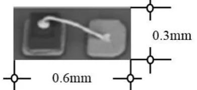
Fig. 1. Device SP top view and cross-section view
Device SP is compared in Fig. 2 to the size of a grain, to illustrate the complexity of the process and the device itself with primary consideration on the total package dimension. As the size becomes smaller, process and device complexity become more challenging. Device SP is considered high density as its 6” single wafer is equivalent to 400,000 units compared to conventional device consisting of only 1,000 units. In addition, it is considered as a device with high complexity as state-of-the-art platforms were needed to satisfy its output process.
Fig. 2. Comparison of Device SP to size of a grain
Assembly to Test Full Process Flow
Complete process flow for Device SP starting from Pre-Assembly to Back-end Assembly until Test and Finish and Packing is shown in Fig. 3. It is worth noting that assembly and test process flow varies with the product and the technology [4] [5].
Fig. 3. Device SP process flow
[Gomez* 5(12): December, 2018] ISSN 2349-4506
Impact Factor: 3.799
G
lobal
J
ournal of
E
ngineering
S
cience and
R
esearch
M
anagement
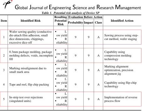
Table 1. Potential risk analysis of Device SPItem Identified Risk
Resulting Potential
Risk
Evaluation Before Action
Identified Action Probability Impact Class
1
Wafer sawing quality (conductive die-attach film adhesion, small dice dimensions, chippings, excessive dice-off
L
ow yield
R
eliability
9 9 A Sawing process using step-cut method, wafer staging
2
0.3mm package molding, package molding defects, voids, incomplete fill
L
ow yield
R
eliability
9 9 A
Capability using compression molding technology
3 Marking misalignment due to small mark area
L
ow yield
R
eliability
9 9 A
Marking alignment optimization, precision alignment jig
4 Tape and reel, flip chip packing
L
ow yield
R
eliability
9 9 A Capability using flip-chip technology
5 In-strip test over rejections (singulated units)
L
ow yield
R
eliability
9 9 A Implementation of reverse process flow
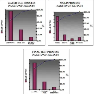
Reject contributors on the identified critical processes are shown in Fig. 4. Wafer Saw, Mold and In-Strip Test or Final Test experienced deviations or output abnormalities as a result of not optimized parameters which are normally attributed to newly introduced device.
Fig. 4. Defect per process contribution
Process Pareto Diagram of Rejects per Critical Process
[Gomez* 5(12): December, 2018] ISSN 2349-4506
Impact Factor: 3.799
G
lobal
J
ournal of
E
ngineering
S
cience and
R
esearch
M
anagement
is one of the factors to be checked as this type of device is to be built for the first time in the plant. Benchmarking for similar device to other sites is being considered to have a baselining on critical process parameters. Fig. 5 also presents the Pareto diagram of reject contribution for the Final Test and Mold processes, respectively, with actual Defect Parts per Million (DPPM) intentionally not given.
Fig. 5. Pareto diagram of rejects showing the top contributor (Actual DPPM values intentionally not shown)
Problem Statement
Top rejects based on Pareto diagram of identified three critical processes substantially affect the yield and delivery during production stressing performance. With this, optimization is highly recommended before it reaches the full production release. Table 2 summarizes the top defect signatures of the critical processes. Further analyses and investigations of failures are made by collecting actual reject samples from critical processes. This will serve as lead in the investigations and formulation of corrective actions.
Table 2. Top defect signature of critical processes
Critical Process Top Defect Signature Criteria Remarks
Wafer Saw
Chippings
Not allowed to reach active
[Gomez* 5(12): December, 2018] ISSN 2349-4506
Impact Factor: 3.799
G
lobal
J
ournal of
E
ngineering
S
cience and
R
esearch
M
anagement
Mold
Voids
Not allowed Failed
Final Test
Auto Align (AA) Fails
Not allowed Failed
REVIEW OF RELATED LITERATURE
Three critical processes of Device SP earlier identified are the Wafer Saw, Mold, and Final Test processes. Details of each critical process and their corresponding top reject contributor are further discussed in this chapter.
Wafer Saw (Critical Process # 1)
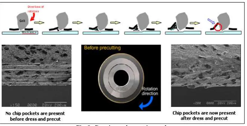
Device SP is considered as Low-K (a material with a small dielectric constant) wafer (very thin), thus sawing becomes a critical process. When abrasive blades cut or groove the material, they are actually grinding and removing it. The mechanism is similar to that of a metal saw: the gaps between the teeth of the saw whisk material away from the point of processing. These gaps, called chip pockets, are encircled in Fig. 6.
Fig. 6. Wafer saw mechanism showing how chipping pockets occur
[Gomez* 5(12): December, 2018] ISSN 2349-4506
Impact Factor: 3.799
G
lobal
J
ournal of
E
ngineering
S
cience and
R
esearch
M
anagement
Fig. 7. Elements of blade structure and their purpose
The blade is composed primarily of grit and bond. The grit is what actually performs the processing. The bond’s role is to the hold the grit in place. Chippings are generally present on a new blade. Hence, blade dressing and precut are needed to be performed, as illustrated in Fig. 8. Blades are dressed before shipment. However, precut operation is still needed to condition the blade and to true the outside diameter, removes excess binder material or loose diamond particles, and minimize the load, creating a cooler and freer cut resulting to minimize occurrence of chippings.
Fig. 8. Dressing and precutting mode
[Gomez* 5(12): December, 2018] ISSN 2349-4506
Impact Factor: 3.799
G
lobal
J
ournal of
E
ngineering
S
cience and
R
esearch
M
anagement
Fig. 9. Step-cutting method
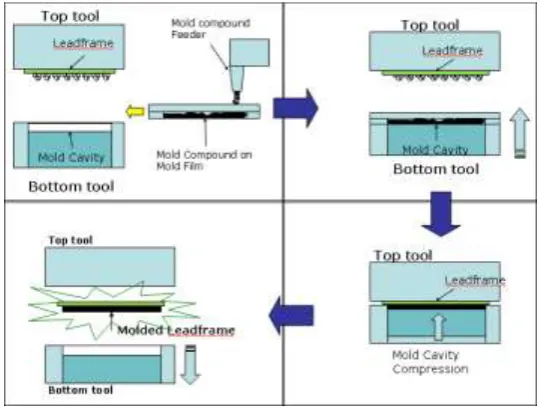
Compression Mold (Critical Process # 2)
One of the integral components in the production of semiconductor Integrated Circuits (IC) is the molding compound [8], a packaging material for encapsulation to protect the IC from external environment. Unlike conventional transfer molding, Device SP process uses compression molding [9] with ultra-fine filler compound, shown in Fig. 10.
Fig. 10. Compression molding mechanism
[Gomez* 5(12): December, 2018] ISSN 2349-4506
Impact Factor: 3.799
G
lobal
J
ournal of
E
ngineering
S
cience and
R
esearch
M
anagement
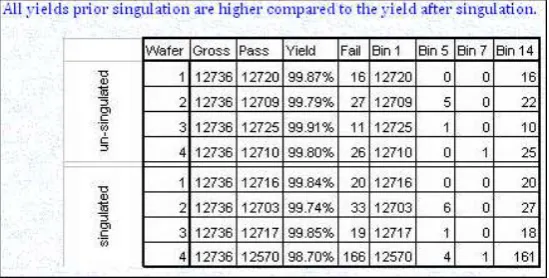
In-Strip Test (Critical Process # 3)Conventionally, units are tested after singulation, but in limited quantity. In this era of technological advancements of high density device, In-Strip Testing was developed. The dilemma however is the contacting issues, as illustrated in Fig. 11. Device SP is consist of 12,740 singulated units making it prone to alignment failures compared to conventional device consisting of less than 500 units.
Fig. 11. Singulated units showing narrow gaps in between units, resulting to auto align (AA) failures
METHODOLOGY
To mitigate the chippings, DOE was done on the three input variables at wafer saw, dressing, precutting, and step-cutting mode, as summarized in Table 3.
Table 3. DOE matrix for wafer saw process
Process Run 1 Run 2 Run 3 Run 4 Run 5
Dressing Yes Yes No No Yes Precut No Yes Yes No Yes Step-cut No No Yes Yes Yes
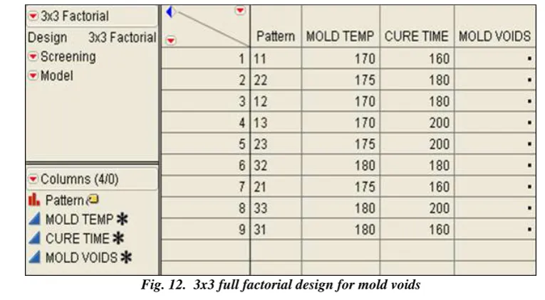
DOE for compression mold was conducted with the objective to determine and define window for critical parameter range, thus eliminate mold voids. Shown in Fig. 12 is the DOE matrix prepared using SAS-JMP [10], a system software calculating automatically the combination of runs.
[Gomez* 5(12): December, 2018] ISSN 2349-4506
Impact Factor: 3.799
G
lobal
J
ournal of
E
ngineering
S
cience and
R
esearch
M
anagement
Full factorial design with a total of nine runs was created. At SAS-JMP, mold temperature and cure time were identified as the most critical parameters that will cause mold voids defect. Results of each run will be discussed in the results section.
In order to eliminate alignment issues, reverse flow was employed. The reverse flow which is testing prior singulation will ultimately resolve Auto Align and other singulation related defects as testing will be done on a strip form. Table 4 shows the matrix to help identify and address the AA failure.
Table 4. 4M+1E matrix to identify and address AA failures, with significant factors denoted in *
Man Machine Method Material Environment
Prober operator Prober Strip loading * Strip * N/A Singulation operator Sawing machine Strip sawing * Blade N/A
Strip mount operator Strip mounter Strip mounting * Mounting tape N/A Mounting jig *
Sawing before testing * N/A
RESULTS AND DISCUSSION
Optimum process parameters were attained based on the results of the DOE that addressed the top reject contributors to the critical processes. Comparative tests were used to statistically validate the results, with the aid of SAS-JMP, a statistical software which greatly facilitates in analyzing the data and relieves much of the tedious calculation. All-Pairs Tukey-Kramer test was preferably used to give a more conservative estimate of results as compared to the other tests.
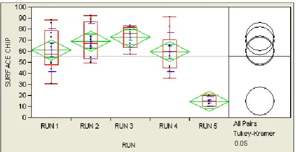
Wafer Saw Optimization to Address Die Chippings
DOE results confirmed that when blade is Dressed, Precut and used Step-Cutting mode, it gives minimal surface chippings. Fig. 13 shows the statistical results with All-Pairs Tukey-Kramer test revealing a highly significant difference on Run 5 in terms of surface chippings among other runs.
Fig. 13. Statistical graph of analysis of variance implying significant difference on Run 5
Compression Mold Optimization to Address Voids
[Gomez* 5(12): December, 2018] ISSN 2349-4506
Impact Factor: 3.799
G
lobal
J
ournal of
E
ngineering
S
cience and
R
esearch
M
anagement
Fig. 14. DOE Matrix to optimize voids during compression molding process
DOE results of compression molding showed that optimum parameters in terms of voids can be achieved by using the 175 degrees Celsius and 180 seconds curing time regardless of molding compound used.
In-Strip Test Optimization to Address AA Fails
Fig. 15 presents the comparable yield and test results during preliminary evaluations when reverse flow is implemented without AA failures.
Fig. 15. Yield comparison of un-singulated vs. singulated units causing AA fails
Although preliminary evaluations were made, large scale validation is needed as reverse flow is considered major change and will undergo process change review. It will take a longer time to implement due to its major change requirements. AA fails was still further investigated while waiting for the reverse flow to be put in place. Cause and effect matrix was tabulated to identify other factors contributing to this defect.
[Gomez* 5(12): December, 2018] ISSN 2349-4506
Impact Factor: 3.799
G
lobal
J
ournal of
E
ngineering
S
cience and
R
esearch
M
anagement
Table 5. Solution validation matrixPotential Causes Actions Error Proofing Level Status
Excessive vacuum force on prober chuck
Install air regulator / vacuum reducer
near chuck area 2 Implemented Insufficient edge stopper to
prevent block from moving during mounting
Redesign mounting jig with edge stopper to prevent block from moving during mounting
2 Implemented Too many air voids in between
unit and tape upon mounting Cleaning of block prior mounting 3 Implemented Movement of singulated units
causing AA failures
Implementation of reverse flow Implement testing prior singulation process
1 Implemented
Verification of Results
After the implementation of the identified solutions, level of rejections was monitored. Shown below in Fig. 16 are the results before and after the solution implementation.
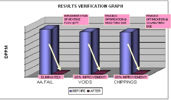
Fig. 16. Improvement after implementation of the corrective actions (Actual DPPM values intentionally not shown)
Significant reduction in the level of rejects were achieved and the three critical processes and their corresponding top reject contributor become stable after the implementation of corrective action. A Poka-Yoke approach by reverse flow lead to the elimination of AA Fails and a remarkable improvement of 95% gained after the implementation of corrective actions for voids and chippings through comprehensive DOE. This is a good indication of manufacturing preparedness for full production mode.
CONCLUSIONS AND RECOMMENDATIONS
[Gomez* 5(12): December, 2018] ISSN 2349-4506
Impact Factor: 3.799
G
lobal
J
ournal of
E
ngineering
S
cience and
R
esearch
M
anagement
It is recommended that the corrective actions identified, sustained, and monitored to maintain the rejects on the acceptable PPM level as some of the identified rejects cannot be zeroed out or eliminated. This technical paper showed how to dig and identify contributing factors on the top rejects of critical processes during early stage of production and employing in-depth engineering and statistical analysis to attain significant improvements and recommends a permanent fix to production line. It is imperative that when new devices are coming in, critical processes are needed to be identified and that appropriate corrective actions and solutions be made so that when full production are set, deliveries will not be at stake.
It is also highly recommended, if not necessary, that the assembly manufacturing processes observe proper ESD controls. Opportunities presented in [11] [12] could be very useful to help ensure ESD check and controls. Ultimately, continuous improvement is important for sustaining the quality excellence of any product and of the assembly plant.
ACKNOWLEDGMENT
The authors would like to express gratitude to STMicroelectronics Calamba New Product Introduction Team and to the Management Team for the extended support.
REFERENCES
1. Tsukada Y, Kobayashi K, Nishimura H. Trend of semiconductor packaging, high density and low cost. 4th International Symposium on Electronic Materials and Packaging, Taiwan; December 2002. 2. Liu Y, Irving S, Luk T, Kinzer D. Trends of power electronic packaging and modeling. 10th
Electronics Packaging Technology Conference, Singapore; December 2008.
3. Sumagpang A, Rada A. A systematic approach in optimizing critical processes of high density and high complexity new scalable device in MAT29 risk production using state-of-the-art platforms. Presented at the 22nd ASEMEP Technical Symposium, Manila, Philippines; June 2012.
4. May GS, Spanos CJ. Fundamentals of semiconductor manufacturing and process control. 1st ed., Wiley-IEEE Press, USA; May 2006.
5. Doering R, Nishi Y. Handbook of semiconductor manufacturing technology. 2nd ed., CRC Press, USA; July 2007.
6. DISCO Corporation. Electroformed bond hub blades – high performance hub blades that take on the challenges of cutting. https://www.disco.co.jp/eg/products/catalog/pdf/nbczh.pdf.
7. DISCO Corporation. Fully automatic dicing saw – advanced performance for 300mm dicing.
https://www.disco.co.jp/eg/products/catalog/pdf/dfd6361.pdf.
8. Ardebili H, Zhang J, Pecht M. Encapsulation technologies for electronic applications, 2nd ed., William Andrew Applied Science Publishers, Elsevier, USA; October 2018.
9. TOWA Corporation. Compression molding system PMC 1040 operational manual. 1st ed., Kyoto, Japan; September 2008.
10. SAS Institute Inc. JMP statistical discovery software. https://www.jmp.com/en_ph/software.html
11. Gomez FR. Improvement on leakage current performance of semiconductor IC packages by eliminating ESD events. Asian Journal of Engineering and Technology, vol. 6, no.5; October 2018. 12. Gomez FR, Mangaoang T. Elimination of ESD events and optimizing waterjet deflash process for