i tif c n e C i o c n S f l e a r n e o n i c t e
a 2
nr 0
et 1
1
n I
ISC 2011
Proceeding of the International Conference on Advanced Science,
Engineering and Information Technology 2011
Hotel Equatorial Bangi-Putrajaya, Malaysia, 14 - 15 January 2011
ISBN 978-983-42366-4-9
ISC 2011
International Conference on Advanced Science, Engineering and Information Technology
ICASEIT 2011
Cutting Edge Sciences for Future Sustainability Hotel Equatorial Bangi-Putrajaya, Malaysia, 14 - 15 January 2011
SR
IE AV IUN IT NESIE
DOKB
IN N
R AG
JA A L S A A E N P M N A A L U A T Y A S
S A I
REPNOI TAI COSSA STNEDUTS NA ISENODN I Organized by Indonesian Students Association Universiti Kebangsaan Malaysia
Proceeding of the
Design and Simulation of Stage
Single-Switch Input-Current Shaping Circuit for AC/DC
Converter Based on PWM Technique
Mahmoud Milad Alageli, Moustafa Mohamed Abdalla, Amer ZerekEngineering Academy, Tajoura P.O.Box 30797, Tajoura, Libya
Tel.:+218213698819, E-mail: [email protected]
Abstract— In this paper a simple single-stage single-switch input-current shaping (S4ICS) circuit was designed, simulated and tested for AC/DC converter which generates input current harmonics due to its non-linear characteristics. A sinusoidal input current with nearly unity distortion factor was achieved through current harmonics mitigation by using PWM boost regulator. The circuit utilizes the charging and discharging increments of boost inductor current to shape a sinusoidal input current. Inductor current was controlled by means of PWM controller. The controller accepts two feed back signals, the first is the inductor current and the other is the output voltage of the AC/DC converter. The simulation results of fast fourier transform FFT show a grate reduction in current harmonic which in turns tends to a grate improvement in power factor and the sinusoidal shape of input current.
Keywords— Boost regulator, Continuous conduction mode, Current harmonics, Current shaping, Power factor, Pulse width modulation.
I. INTRODUCTION
Currently, the electrical power industry has grown rapidly and loads are changing from simple, non-electronic loads such as tungsten lamps, motors, relays and resistive heaters to electronic ones such as fluorescent lamps, motors with solid state switching devices. These electronic loads (also known as non-linear loads which draw a non-sinusoidal current even when the supply voltage is perfectly sinusoidal) [1] are the major sources of excessive current harmonics which leads to power quality PQ pollution introduced in electrical grids. The current harmonics has a significant effect on customer loads in a form of heating, distortion or operation malfunction.
Harmonic disturbances are the most researched part of all power quality disturbances, especially over the past two decades. The interest in harmonics research can largely be attributed to the advance in power electronics technologies, and this driven by the desire to have more energy efficient equipment and greater control of equipment operation. Input-Current shaping, power factor correction PFC and harmonics mitigation technologies are all inherently related to each other and can be essentially classified into two main categories: passive methods and active methods.
The first methods are simply based on the use of RLC filter that offer a low impedance path for unwanted current harmonics and drive it back away from the load under consideration. These filters have no switches and hence no electromagnetic interference emissions EMI. Beside that it is very simple, robust and has low cost of implementation. However, their performance lower when compared to active circuits, they are heavy bulky specially when designed for low harmonics mitigations. Passive filters are employed either to shunt the harmonic currents off the line or to block their flow between parts of the system by tuning the elements to create a resonance at a selected harmonic frequency [2].
converters filters that usually applied to the circuits that contain AC to DC converter such as DC motor drive, switched mode power supply and battery chargers. In these types of current wave shaping technique, line current is forced to follow the sinusoidal line voltage. A controlled high frequency pulse width modulation (PWM) applied on the DC-DC converter which is the main component of the circuit
Standardization activities in this area of harmonics limitation have been carried out for many years. As early as 1982, the International Electrotechnical Committee – IEC published its standard IEC 555-2, which was also adopted in 1987 as European standard EN 60555-2, by the European Committee for Electrotechnical Standardization - CENELEC. IEC 555-2 standard has been replaced in 1995 by standard IEC 1000-3-2, also adopted by CENELEC as European standard EN 61000-3-2 (IEC Standards 1998). Standard IEC 1000-3-2 applies to equipment with a rated current of up to and including 16A rms per phase which is to be connected to 50Hz or 60Hz, 220-240Vrms single-phase, or 380-415Vrms three-phase mains [4].
II. THE PROPOSED CIRCUIT
The proposed S4ICS circuit is designed for AC-DC converter and it considered as nonlinear load. The S4ICS circuit is essentially based on boost DC-DC regulator with high frequency PWM controller. The controller gets two control signals and generates the PWM switching pulses accordingly as shown in Fig. 1.
Feeding the input current reference signal and the DC voltage ripple reference into the switching controller will yield both harmonic reduction and DC voltage regulation. The principle of operation for DC-DC switching regulator harmonic filtering is related to the topology of DC-DC converter through which PWM is performed. Among the different power regulators topologies boost converter shown in Figure.1 is the most suitable one, where the boost inductor is in series with the ac power line. This result in minimum conducted electromagnetic interference (EMI) at the line when the circuit operates in continuous conduction mode (CCM) [5].
For our boost regulator topology, the input current shaping is performed by controlling the amplitude of boost inductor current, and this in turns is done through the controlling or the modulation of switching pulses.
When the boost switch is turned ON, the inductor current tends to rise due to charging of boost inductor, and when the switch turned OFF, the inductor current will decay down by discharging through boost capacitor. The rise increment is given by equation.(1) [6]. These increments up and down of boost inductor current are the key of current shaping as shown in Fig 2.
s
iL LF
D t
v()
2
(1)
where
i Increment in inductor current
v(t) Instantaneous phase voltage
D Duty cycle of boost switch
L Boost inductor
Fs Switching frequency of boost converter
Fig.1S4ICS Circuit Utilizing Boost DC-DC Switching Converter
Fig.2 Simulation Shows How the Boost Inductors Ripples Follow the Sinusoidal Reference
III. POWER STAGE DESIGN
The parameters of the designed power stage are listed in Table.1, in which the converter parameter include boost inductance boost capacitance, and also input line voltage, DC output voltage and rated power.
A. Boost Inductance
It is one of the keys components in the design. The value of this inductor significantly affects the ripple current due to switching operation of boost converter. Inductance value was calculated to give an acceptable level of peak to peak ripple current which is chosen between 10% and 20% of the input current peak value. The value of boost inductance also affect the regulator’s mode of operation, higher inductance value moves the regulator to work in discontinues conduction mode DCM mode where the current does reach the zero level which not preferred due to its EMI pollution. Equation (1) can be used to calculate boost inductance.
For the values of line voltage = 110 V rms, output DC voltage = 300 V, input current = 9.82 A rms and switching frequency of 20 K Hz, the inductance value is calculated and found to be 1 mH.
TABLE I
PARAMETERS OF THE DESIGNED POWER STAGE
Parameter Value line voltage
DC output voltage Motor power Boost inductance Boost capacitance
B. Boost Inductance
The capacitance was calculated using the formula in equation 2. [8],
2 2 2 1 2
V V
Pt
C HLD
OUT (1)
Where
COUT Boost capacitance
P Rated output power
tHLD Holdup time
V1 Capacitor voltage at the beginning of HLD t
V2 Capacitor voltage at the end of HLD t
The parameters that affect the choice of the boost capacitance include:
1) Hold-up time: capability which is the amount of time at
rated output power that will take the capacitor voltage to discharge to a minimum operating voltage.
2) Output DC ripples current.
For hold-up time of 20 ms, V1 at the rated output DC voltage, V2 of 290 V and rated power of 1 KW, the boost capacitance is calculated to be 6200 μF.
IV. POWER CONTROLLER DESIGN
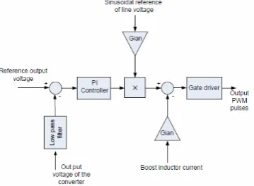
PWM controller responsible of generating switching pulses for boost regulator to perform two functions; sinusoidal current shaping and maintaining constant and stable output voltage. For this reasons the controller is designed with two feedback signal, one from output voltage of the converter and the other from input line current which is equivalent to boost inductor current as shown in Fig. 3.
Low pass filter is used to control the out put ripple voltage of the converter and the reference voltage is used to select the required level of output voltage. Sinusoidal reference is taken as pattern over which the line current is shaped. Gains are used to modify the signal to next controlling stage. The error signal that used as an input for gate driver is generated from comparing the boost current with modified sinusoidal reference after the product. Gate driver generate positive pulse when the error is positive and zero voltage when the error is negative and it works as PWM modulator.
The paper will not be reformatted, so please strictly keep the instructions given above, otherwise it will be returned for improvement. Please upload your paper in PDF file through the Conference website under Paper Submission menu. Papers sent by e-mail will not be processed.
Fig. 3 PWM Controller with two Feed Back Loops
V. SIMULATION RESULTS
Simulink model was used to simulate a S4ICS circuit for single phase AC/DC converter; The fast Fourier Transform FFT analysis was applied to calculate the harmonic content of the input current before and after input-current shaping.
Fig. 4 shows the input line current after the input-current shaping, it is clear that the current tends to rush up at the beginning of operation for a part of half cycle. This is because the output capacitor is empty of charge and works as short circuit at that point. This problem can be solved by using a soft starting circuit which is out of our scope.
In Fig. 5, the inductor current (input current) appears as saw tooth due to charging and discharging phases of boost inductance. The conduction point between charging and discharging is kept at none zero value which indicates that the converter works in CCM.
Fig. 4 Shows the Input Line Current after Input-Current Shaping
Fig. 5 Inductor Current Made of Charging and Discharging Phases
visually from a sinusoidal shape of the current and numerically for the result of FFT analysis.
The FFT analysis was applied to the input line current generated by the Matlab simulation model. Analysis was performed before and after input-current shaping.
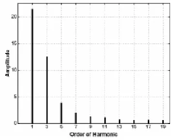
The harmonics plot prior to the input-current shaping is shown in Fig. 7. The AC/DC converter without input-current shaping is composed of bridge rectifier followed by boost regulator work at operating frequency of 2 KHz, duty cycle is calculated to maintain the out put voltage at 300V. The results show that the boost regulator works at DCM with current drown at fraction of line voltage cycle. This leads to a significant 3rd up to 7th harmonics of 12.59 V, 3.9 V and 2.02 V respectively. Exact odd harmonic levels are listed in Table 2. Different RMS values of input current are given in Table 3.
Fig. 6: Shows the Input Current Plotted over the Line Voltage.
Fig. 7 Significant Odd Harmonics Plot Prior to the Input-Current Shaping
TABLE II SIGNIFICANT ODD HARMONICS LEVELS PRIOR TO THE INPUTCURRENT SHAPING
Harmonic
Order 1st 3rd 5th 7th 11th 19th
Harmonic Amplitude
in A 21.5 12.59 3.9 2.02 1.19 0.86
TABLE III RMS VALUES OF THE CURRENT BEFORE INPUT-CURRENT SHAPING
Total RMS Current Fundamental RMS Current Harmonics RMS Current
17.98 A 15.22 A 9.58 A
Input-current shaping is achieved by using inherent boost DC-DC switching regulator in which harmonics levels were significantly reduced. Fig. 8 shows the odd harmonics plot after input-current shaping. Exact odd harmonic levels are listed in Table 4. Different RMS values of input current are given in Table 5.
Fig. 8 Odd Harmonics after Input-Current Shaping
TABLE IV SIGNIFICANT ODD HARMONICS LEVELS AFTER INPUT-CURRENT SHAPING
Harmonic
Order 1st 3rd 5th 7th 11th 19th
Harmonic Amplitude
in A 14 0.27 0.83 0.67 0.54 0.26
TABLE V RMS VALUES OF THE CURRENT AFTER INPUT-CURRENT SHAPING
Total RMS Current Fundamental RMS Current Harmonics RMS Current
10.17 A 10.07 A 1.43 A
The significant 3rd up to 7th harmonics were mitigated
from 12.53 V, 3.9 V and 2.02 V to 0.27 V, 0.55 V and 0.83 V. The harmonic of higher frequencies in the range of switching frequency of DC-DC boost regulator can be filtered easily with small shunt capacitor. Harmonics mitigation results in a huge improvement in the shape of current waveforms and the power factor improved from 84.64 % to 99.01 %
VI. CONCLUSION
A Single-Stage Single-Switch Input-Current Shaping
(S4ICS) circuit using pulse width modulated PWM boost
and shows good result in input-current shaping (harmonic mitigation) and output voltage regulation. Harmonics mitigation results in a huge improvement in power factor which improved from 84.64 % to 99.01 %.
REFERENCES
[1] Tristan, A. K., P.E, “Distortion and Power Factor of Nonlinear
Loads.” LTK Engineering Services: 0-7803-5533-4/99/$10.00, 1999
[2] Bernard, S., “Harmonics Pollution” www.powers
quality.com/art0041, 1995
[3] Akagi, H., “New Trends in Active Filters for Power Conditioning”.
IEEE Transaction on Industry Applications, 1996
[4] IEC 1000-3-2 (1995-3) Ed.1, “Electromagnetic Compatibility (EMC)
-part 3-2: Limits for harmonic current emissions (equipment input
current ≤16a Per phase) “. IEC., 1995
[5] Zhou, C., Raymound B. R. & Fred C. L., “Design and Analysis of a
Hysteretic Boost Power Factor Correction Circuit”. IEEE, 1990
[6] Phillip C. T., “Boost Power Factor Corrector Design with the
UC3853 ”. ©, Texas Instruments Incorporated., 1999
[7] Fairchild, “Theory and Application of the ML4821 Average Current
Mode PFC Controller” . REV 1: 0 10/25/2000, 1997
[8] Harding, J., “Off-Line Power Supply Using the Farm Ac Front-End