Missouri University of Science and Technology Missouri University of Science and Technology
Scholars' Mine
Scholars' Mine
Electrical and Computer Engineering Faculty
Research & Creative Works Electrical and Computer Engineering
25 Jul 2019
Microwave Reflectometry for Physical Inspections
Microwave Reflectometry for Physical Inspections
Mohammad Tayeb Ahmad Ghasr
Missouri University of Science and Technology, [email protected]
R. Zoughi
Missouri University of Science and Technology, [email protected]
Satyajeet Shinde Sasi Jothibasu
Follow this and additional works at: https://scholarsmine.mst.edu/ele_comeng_facwork
Part of the Electrical and Computer Engineering Commons
Recommended Citation Recommended Citation
M. T. Ghasr et al., "Microwave Reflectometry for Physical Inspections," U.S. Patents, Jul 2019.
This Patent is brought to you for free and open access by Scholars' Mine. It has been accepted for inclusion in Electrical and Computer Engineering Faculty Research & Creative Works by an authorized administrator of Scholars' Mine. This work is protected by U. S. Copyright Law. Unauthorized use including reproduction for redistribution requires the permission of the copyright holder. For more information, please contact [email protected].
Ghasr et al .
( 43 ) Pub . Date :
Jul
. 25 , 2019
( 54 ) MICROWAVE REFLECTOMETRY FOR
PHYSICAL INSPECTIONS
Publication Classification
( 51 ) Int . Ci
.
GOIN 22 / 00( 2006 . 01 )
GOIR 27 / 06
( 2006 . 01 )
( 52 ) U . S . CI .
CPC . . . GOIN 22 / 00 ( 2013 . 01 ) ; GOIR 27 / 06 ( 2013 . 01 )( 57 )
ABSTRACT
( 71 ) Applicant : The Curators of the University of
Missouri
, Columbia , MO ( US )
( 72 ) Inventors : Mohammad Tayeb Ghasr , Rolla , MO
( US ) ; Reza Zoughi
, Wildwood , MO
( US ) ; Satyajeet Shinde , Rolla , MO
( US
) ; Sasi Jothibasu , Rolla , MO ( US )
( 21 ) Appl . No
. :
16 / 326 , 529
( 22 ) PCT Filed :
Aug . 18 , 2017
( 86 ) PCT No
. :
PCT
/ US17 / 47489
$ 371 ( c ) ( 1 ) ,
( 2 ) Date :
Feb . 19 , 2019
Related U . S . Application Data
( 60 ) Provisional application No . 62 / 377 , 387 , filed on Aug .
19 , 2016 .Utilizing microwave reflections to compare a reference
device with counterfeit and / or aging devices under test . The
reflection from the device under test varies based on certain
properties , which results in each device having a unique and intrinsic electromagnetic signature . Comparisons of the electromagnetic signature of the device under test to the
electromagnetic signature of a reference device enable
evaluating the acceptability of the device under test .
100
or mon non SIGNAL SOURCE 102 PROBE 104 DEVICE UNDER TEST 106 M WW MEASURING DEVICE108
ooooooooooooooo
PROCESSOR PROCESSOR READABLE STORAGE DEVICE 112nnnnnnnnnnnnn
OOOOOO
DISPLAY 114Patent Application Publication Jul . 25 , 2019 Sheet 1 of 13
US 2019 / 0227003 A1
FIG . 1
100
wwwwwwwwwwwwwwwwwwwwwwwwww wwwwwwwwwwPROBE
SIGNAL SOURCE
102
DEVICEUNDER TEST
104
0800 8888 8888 88MEASURING DEVICE
OOOOOOOOOOOOO000 . 000 000 000 OOOOOOOOOOOOOPROCESSOR
READABLE STORAGE
DEVICE
PROCESSOR
DISPLAY
FIG . 2
104
??????????????????????? ? ~ . . } . . . . . . . ~ . . . ?? ?? ?? ?? ?? ?? ?? 3 ?? ?? ?? ?? ?? ?? 8???
?????????????????????????????????????????????????????????????????
Patent Application Publication Jul . 25 , 2019 Sheet 3 of 13
US 2019 / 0227003 A1
FIG . 3
00000000
- 302
306
304 mm
~ 308
306
FIG . 4
POSITION / ORIENT DEVICE UNDER TEST
22222222 2 2 2 2 2 2222
402
TRANSMITELECTROMAGNETIC SIGNAL TO
IRRADIATE DEVICE UNDER TEST
404
222222222222222
RECEIVE REFLECTED ELECTROMAGNETIC
SIGNAL
406
2222222222222222
????????????????????????????????????????????????????????????????????????????????????????????????????????????????????????????????????????????????????????????
MEASURE REFLECTION COEFFICIENT
DETERMINE ELECTROMAGNETIC
SIGNATURE
DETERMINE QUANTITATIVE METRIC
412
Oto
VYYYYYYYYYYYYYYYYYYYYYYYYYYYYYYYYYYE
ELECTROMAGNETIC SIGNATURE TO
COMPARE DETERMINED
KNOWN ELECTROMAGNETIC
FIG
.
5A
FIG
.
5B
S . .0000000000000000000000000000
Patent Application Publication
CB4011BE
-
NEW
SA556N
CB4011BE -
NEW
powe SA556N
- 0Titti
1 : 11 : ! * * * * * * * www . . 0 , 8 - 0 6 - 0 . 4 - 0 . 2 olo 02 0 . 4 0 . 6 0 . 8 - 0 . 8 - 0 . 6 - 0 . 4 - 02 00 OR 10 . 4 0 . 6 0 . 8CB4011BE
-
NEW
SA556N
-
SA556N
CB4011
BE
-
NEW
Jul . 25 , 2019 Sheet 5 of 13
* httesti
freq
(
18
.
00GHz
to
26
.
50GHz
)
freq
(
26
.
50GHz
to
40
.
00GHz
)
US 2019 / 0227003 A1
FIG . 6A
. . . . . . . . : : . . . : * * * * * . . . . : * * . . . . . . . . 24SN75189N
. . .
US 2019 / 0227003 A1
* EASN68ISENS
. . . . . . . : : : : : : : : : : : : :N98LUVLNS
. . ! ! ' . . . . . . . . . . . . . . . . . . . . . . . . . . . . . . : : : : : : . . . . ! ! ! ! . ! ! ! ! . . . . . . . " . ' . ' . . . . . . . .Jul . 25 , 2019 Sheet 7 of 13
. . : . : . : . : . : . : . : . : : . . . . ' ' . . . . . . . . . . " . . . . . . 3 . . . . . . . . ' . . . . . . . . . . . . . .Patent Application Publication
. . . TE
FIG . 6B
: : : :3 gius gogo
FIG . 7A
100000000000000000000000000000000000000 XXXXXXFIG . 7B
DOOOOOOOPatent Application Publication Jul . 25 , 2019 Sheet 9 of 13
US 2019 / 0227003 A1
FIG . 7C
3 . . . . . . : . : . . . . . . . .WA
mu MEAN VALUE
. : . : . : . : . : . : . : . : . : . : . : . : . . : : . : . : . : . : . : . : . : . : . : : . : . : : . . : . : : : : . . . . . . . : . : . . . . . . . . . . . . . . . . . . . . . . . . :MEAN VALUE
: : : . : . : : . . : . : : : : : : : : : : : : : : : : : : : : : : : : : . .TL497ACN
FIG . 7D
0 . 045
( b ) Ka - band
. . : . : . .A
MEAN VALUE
SMEAN VALUE
. : : . : : . : . : . : . : . : . : : : . : : : . . . . : : : : : : : : : : : :0 . 025 . . .
. . . . . . . . . . . . . . . . . . . . . i i. . . . . . . . . . . . . . . . . . . . . . . . .
FIG . 8A
FIG . 8B
MEAN VALUE
Y XHEC . ' . c . C . . . . . . . . . . . . . . . 11 : 11 : 12 . . . . . . . . . . . . . . . . . . . . . . . . . . . . . . . . . . . : : . : . : . . . . . . . . . . . . . . . . . . . . . . . . . . . . . . . . . . . . .- MEAN VALUE
. . . . . . . . . . . . . . . . . . . . . . . . . . . . . . . 00000000000000000000000000000000000000000FIG . 8D
UA723CN
LLA723CN
$ . . . : : . . . : . : . : . : . : . : : . : . : : . : . : .- MEAN VALUE
. . . . . . . . , i . * . * * * * * . . . . . . . . . . . . . . . . . . . . . . . . . . . . . . . . . . . . * WWW . . ' ' . ' ' indd . . . . . . . . . ' , ' ' , ' , ' . . , ' ' , ' , ' * * * * * * * * * * . W . . . . ' .wwwwwwwwwwwwwwwwwww
. : : : : : . . . . . . . . . : : : . . : . : . : . : . . : : : . . . . . . . ' , ' ' , ' ' , ' ' , ' ' , 'MEAN VALUE
* , ' ' , ' . ' . . ' ' . * * : . . . . . . . , , , , , , , LLLLLLLLLLLLLLLLLLLLLL . IIIIIIIIIIIIIIIIIIIIIIIIIIIIIIII . . . . . . . : : :FIG . 8C
US 2019 / 0227003 A1
Jul . 25 , 2019 Sheet 11 of 13
FIG . 9A
Patent Application Publication Jul . 25 , 2019 Sheet 13 of 13 US 2019 / 0227003 A1
FIG . 9C
99999999999 W 999999gogoooooooooo . . . . . . . . . . . . . . ' : : 1 : . . : : : : : : : : : : : : : : : : : : : : : : : : : . .- MEAN VALUE
. . .0 . 02 .
E " : : . . P . ' ' ' . ' , , ' , ' ' , ' . . . . . . . . . . . . . . ' . . " : ? : . : : . . : . .pun MEAN VALUE
" - : : . . . " - - : . . . . . . : . .van armari ini
: . : iii . 1 ' . . . . . . . . . . . . . . . . . . . . . WY XX
FIG . 9D
ooooooo : . . . . . . . : : : : : : : : : : : : : : : : : : : . . . . . . . . . . . . . . . .- MEAN VALUE
. . . . . . . . . . . . . . . . . . . . . . . . . . . . . in www . . . . : : : : : . : . . : . : . : . : . : . : . : . : : : : W0 . 02
. . . .- MEAN VALUE
' : . . . . . . . . . . . . . . : . . : : : : . . . . . . . . . . . . . . . . . . . . : . . . : : : : : . : : . : . : . : . : . : : . : . : : . : . : . : . : .MICROWAVE REFLECTOMETRY FOR
PHYSICAL INSPECTIONS
CROSS REFERENCE TO RELATED
APPLICATION
[ 0001 ] This application claims the benefit of U . S . Provi
sional Patent Application No . 62 / 377 , 387 , filed Aug . 19 ,
2016 , the contents of which are incorporated by reference in
their entirety for all purposes .
BACKGROUND
[ 0002 ] Electronic devices and components that are coun
terfeit , tampered with , cloned , aged , and / or manufactured in
a substandard manner present various significant problems
and risks , such as unexpected failure , disruption in service ,
unreliability , unauthorized exploitation , and / or compro
mised safety and security . Exemplary electronic devices
include integrated circuits , capacitors , resistors , and non
linear devices ( e . g . , detectors , fast switching PIN diodes , varactor diodes , etc . ) . There are many properties of a certain
device that may cause it to be considered unacceptable for
use in products . Moreover , properties ( e . g . , shape , size ,
electronic characteristics , etc . ) vary among many types of
devices . These variabilities create significant challenges to quickly and accurately determining whether a particular
device is acceptable for use .
different characteristics from a magnitude and a phase of the
transmitted electromagnetic signal . The electronic device is
aligned relative to the waveguide . The measuring instrument
is coupled to the probe and configured to measure a complex
reflection coefficient as a function of frequency of the
reflected electromagnetic signal . The reflection coefficienthas a magnitude and a phase . The processor is configured to
determine an electromagnetic signature of the electronic
device as a function of the measured complex reflection
coefficient relative to one or more known electromagneticsignatures .
[ 0006 ] In yet another aspect , a method for non - destructive
detection of counterfeit electronic devices includes an
antenna transmitting an electromagnetic signal that includes
at least high - frequency electromagnetic energy incident
upon an electronic device aligned relative to the antenna . The antenna receives an electromagnetic field reflected from the electronic device . The reflected electromagnetic field has a magnitude and a phase that differ from a magnitude and a
phase of the transmitted electromagnetic signal . A measur
ing device measures a complex reflection coefficient as a
function of frequency of the received electromagnetic field
referenced to the antenna . The complex reflection coefficient is spatially and spectrally integrated . A processor executing
an algorithm determines a quantitative metric from the
measured complex reflection coefficient for comparison to
another quantitative metric determined from one or more
known electromagnetic signatures .
[ 0007 ] This Summary is provided to introduce a selection
of concepts in a simplified form that are further described
below in the Detailed Description . This Summary is not intended to identify key features or essential features of the claimed subject matter , nor is it intended to be used as an aid in determining the scope of the claimed subject matter .
[ 0008 ] Other features will be in part apparent and in part
pointed out hereinafter .
SUMMARY
[ 0003 ] Briefly , aspects of the present disclosure utilize
microwave reflections to distinguish between a reference
device ( e . g . , integrated circuit , or IC ) and counterfeit and / or
aging devices under test . The reflection from the device
under test varies based on certain properties ( e . g . , internal IC
package interconnect layout , bond wire routing , IC casing
material , presence / absence of silicon die , etc . ) . These prop
erties result in each device having a unique and intrinsic
electromagnetic signature . Comparisons of the electromag
netic signature of the device under test to the electromag netic signature of a reference device enable evaluating the acceptability of the device under test .
[ 0004 ] In an aspect , a method of evaluating a device under
test ( DUT
) includes irradiating a DUT with a first electro
magnetic signal . The first electromagnetic signal includes
electromagnetic energy having a microwave or higher fre
quency . A second electromagnetic signal is received , which includes the electromagnetic energy of the first electromag
netic signal reflected by the DUT
. A measuring device
measures a reflection coefficient associated with the DUT as
a function of frequency of the second electromagnetic
signal . An electromagnetic signature of the DUT is deter mined as a function of the reflection coefficient associated with the DUT . The electromagnetic signature of the DUT is compared to one or more known electromagnetic signatures
to evaluate the DUT .
[ 0005 ] . In another aspect , a system for evaluating an elec tronic device includes a probe , a measuring instrument , and a processor . The probe is coupled to a signal source . The probe also includes a radiating aperture through which an electromagnetic signal generated by the signal source is transmitted to an electronic device located remotely from the
aperture . An electromagnetic signal reflected from the elec
tronic device is also received by the aperture . A magnitude
and a phase of the reflected electromagnetic signal exhibit
BRIEF DESCRIPTION OF THE DRAWINGS
10009 ] . FIG . 1 is a block diagram of an exemplary reflec
tometry system according to an embodiment
.
[ 0010 ] FIG . 2 illustrates an exemplary orientation and
positioning of a device under test according to an embodi ment .
[ 0011 ] FIG . 3 illustrates an exemplary test fixture for
orienting and positioning of an integrated circuit under test
according to an embodiment
.
[ 0012 ] FIG . 4 is a flowchart of an exemplary operation of
a reflectometry system according to an embodiment .
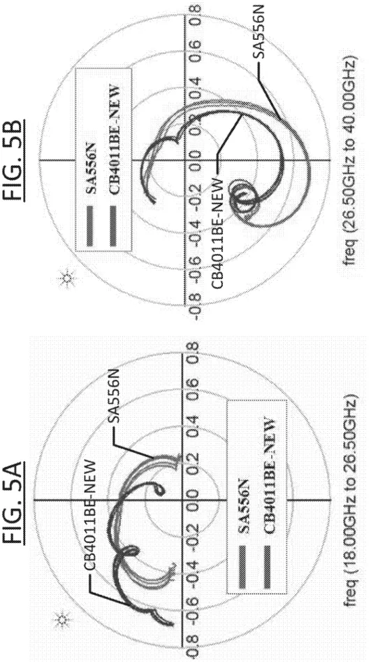
[ 0013 ] FIGS . 5A and 5B illustrate exemplary complex
reflection coefficients , as a function of frequency , between
an integrated circuit under test and a reference integrated
circuit according to an embodiment .
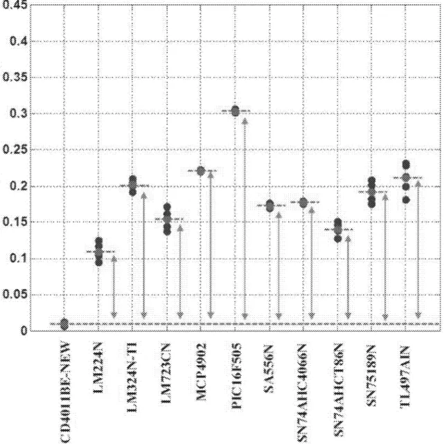
[ 0014 ] FIGS . 6A and 6B illustrate exemplary root - mean
square error values between integrated circuits under test referenced to a mean value of root - mean - square error values
of a reference integrated circuit according to an embodi
ment .
[ 0015 ] FIGS . 7A and 7B are X - ray images illustrating an
internal structure of exemplary DC - DC Boost converter
integrated circuits .
100161 FIGS . 7C and 7D illustrate exemplary root - mean
square error values of the integrated circuits of FIGS
. 7A and
US 2019 / 0227003 A1
Jul . 25 , 2019
[ 0017 ) FIGS . 8A and 8B are X - ray images illustrating an
internal structure of exemplary linear regulator integrated
circuits .
[ 0018 ] FIGS . 8C and 8D illustrate exemplary root - mean square error values of the integrated circuits of FIGS . 8A and 8B .
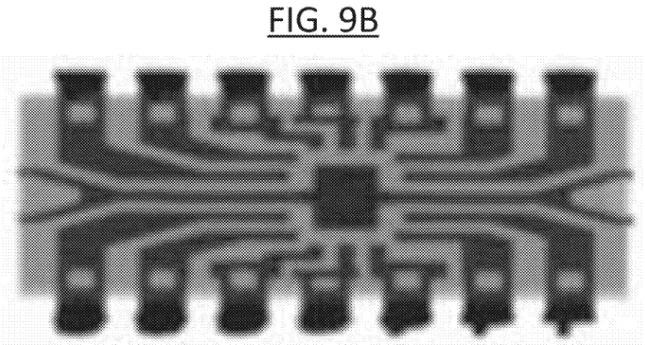
[ 0019 ] FIGS . 9A and 9B are X - ray images illustrating an internal structure of exemplary new and aged NAND gate
integrated circuits .
[ 0020 ] FIGS . 9C and 9D illustrate exemplary root - mean square error values of the integrated circuits of FIGS . 9A and 9B .
[ 0021 ] Corresponding reference characters indicate corre
sponding parts throughout the drawings .
DETAILED DESCRIPTION
[ 0022 ] Electromagnetic ( EM ) signature evaluation tech
niques , using high frequency EM signals , enable determi
nations of authenticity and acceptability of devices under test , such as electronic integrated circuits ( ICs ) , other pas sive and active electronic devices and components , and the like . Aspects of the present disclosure evaluate the intrinsic and unique characteristics of EM signatures of devices in a
“ powered - off ” state . In one form , a device under test is
illuminated / irradiated by an EM field for obtaining a char
acteristic EM signature of the device under test at a given
frequency or band of frequencies .
[ 0023 ] Because of the differences and degrees of variabil
ity that may exist for particular devices under test ( e . g . , packaging material properties , electronic circuit design lay out , etc . ) the distinction between “ acceptable ” and “ unac
ceptable ” devices may not be robustly accomplished in a
deterministic manner . Given the non - deterministic nature ofthese evaluations , statistical EM signature metrics , such as
root - mean - square error ( RMSE ) , enable a determination of acceptability of the device under test . For example , the
characteristic EM signature of a device may be statistically
compared to the EM signature of an " acceptable ” group of the same device . In this manner , a metric related to the
differences between the two classes of EM signatures may
be established by which to determine and decide on the
acceptability of a given device .
[ 0024 ] FIG . 1 illustrates an exemplary reflectometry sys
tem 100 according to an embodiment of the disclosure . The system 100 includes a signal source 102 , a probe 104 , a device under test ( DUT ) 106 , a measuring device 108 , a processor 110 , a processor - readable storage device 112 , and
a display 114 . The signal source 102 is electrically and / or
communicatively connected to the probe 104 . The probe 104 is also electrically and / or communicatively connected to the measuring device 108 ( e . g . , via a coax - to - waveguide adapter ) . The measuring device 108 is electrically and / or
communicatively connected to the processor 110 , which is
in turn electrically and / or communicatively connected to the processor - readable storage device 112 and the display 114 . [ 0025 ] In an embodiment , signal source 102 is adapted to generate and provide a microwave signal to probe 104 ,
which in turn is adapted to transmit microwave electromag
netic energy incident upon DUT 106 . In this manner
, signal
source 102 and probe 104 are adapted irradiate / illuminate
DUT
106 with electromagnetic energy . In one form , the term
microwave as used herein comprises microwave or milli meter wave electromagnetic energy having a frequency
greater than ultra - high frequency . For example , microwave
electromagnetic energy includes electromagnetic energy
having a frequency of about 300 megahertz ( MHz
) to about
300 gigahertz ( GHz
) , such as the K - band ( e . g . , 18 - 26 . 5
GHz
) and / or the Ka - band ( e . g . , 26 . 5 - 40 GHz
) . In an embodi
ment , the transmitted microwave signal is swept over a
range of frequencies ( e . g . , a bandwidth greater than 0 Hz , a
25 GHz bandwidth , etc . ) .
[ 0026 ] The probe 104 is also adapted to receive ( e . g . ,
sample ) an electromagnetic signal reflected from DUT 106
that includes the electromagnetic energy of the transmitted
electromagnetic signal . The probe 104 may comprise an
antenna ( e . g . , a horn antenna , etc . ) , an aperture probe , a
waveguide having an aperture ( e . g . , an open - ended rectan
gular waveguide , etc . ) , an open - ended coaxial probe , and the
like . In an embodiment , probe 104 is adapted to produce a
spatially integrated reflected electromagnetic ( EM ) signa
ture of DUT 106 by averaging the reflected signal over its
aperture . Advantageously , the spatially integrated EM sig
nature enables aspects of system 100 to provide precise
results . In one form , probe 104 comprises a K - band wave guide having dimensions of 10 . 7x4 . 3 millimeters ( 0 . 420x0 .
170 inches ) . In another form , probe 104 comprises a Ka
band waveguide having dimensions of 7 . 11x3 . 56
millimeters ( 0 . 280x0 . 140 inches ) . One having ordinary skill
in the art will understand that probes having varying EM
characteristics and geometries , which offer measurement
flexibility , are within the scope of the present disclosure . In
an embodiment , probe 104 comprises a compact probe array ,
accommodating a plurality of testing spots simultaneously , which is made in the form of substrate - integrated - waveguides ( SIW ) . In this embodiment , each SIW in the array is
relatively small and its pertinent measurement electronic
components can be manufactured using surface - mount and
printed circuit board ( PCB ) technology , making the entire
measurement system small and robust . In an embodiment ,modified waveguide flanges are utilized with probe 104 to reduce unwanted reflections from the edges of the probing waveguide flanges , which enables a more robust reflection
coefficient measurement .
100271 . The measuring device 108 is adapted to measure parameters ( e . g . , network parameters , scattering parameters ,
etc . ) of the electrical network formed by signal source 102 ,
probe 104 , and DUT 106 ( e . g . , transmission and reflection of
EM signals ) . In an embodiment , measuring device 108
measures both amplitude and phase properties . For example , measuring device 108 may comprise a vector network analyzer ( VNA ) , a vector reflectometer , and / or a coherent reflectometer for measuring a complex reflection coefficient ( e . g . , amplitude and phase ) . An exemplary VNA includes an Anritsu 40 GHZ VNA . In another embodiment , measuring device 108 measures amplitude properties only . For example , measuring device 108 may comprise a scalar network analyzer for measuring a real reflection coefficient
( e . g . , amplitude only ) . The measuring device 108 may also
be referred to as a measuring instrument in accordance with
one or more embodiments of the disclosure . In an embodi ment , signal source 102 , measuring device 108 , processor 110 , processor - readable storage device 112 , and display 114 comprise a single measurement device / instrument , such as a VNA . Additionally or alternatively , probe 104 and measur ing device 108 may comprise a single measurement device /
instrument , in accordance with one or more embodiments of
[ 0028 ] The processor 110 is adapted to execute processor
executable instructions stored on processor - readable storage
device 112 to obtain an electromagnetic signature of DUT
106 . In an embodiment , processor 110 executes processor executable instructions comprising an estimation algorithm for determining material characteristics of DUT 106 as a function of the reflected electromagnetic signal received by
probe 104 . In an embodiment in which DUT 106 is an
integrated circuit ( IC ) , the electromagnetic signature or the reflected electromagnetic signal containing properties ( e . g . ,
magnitude and / or phase ) of the IC varies due to different
material properties and / or varied electronic circuitry inside
the IC . For example , the reflection from an IC may vary
based on the internal IC package interconnect layout , bond
wire routing within the IC , IC plastic casing material ,
presence and / or absence of the silicon die within the IC , and
the like .
[ 0029 ] In an embodiment , processor 110 executes proces
sor - executable instructions to develop and associate a quan
titative metric with the differences between the spatially and
spectrally integrated ( e . g . , over the waveguide band ) reflec
tion coefficient characteristics . Such a metric enables rapid
evaluation and comparison of devices under test , such as in
a large throughput manufacturing or testing environment ,
for example . In one form , processor 110 executes processor executable instructions to calculate an LP - norm . In an addi tional or alternative form , processor 110 executes processor executable instructions to calculate a root - mean - square error ( RMSE ) , which is defined as the average Euclidean distance between two reflection coefficient vectors and used as a
quantitative metric to evaluate the integrated degree of
difference between the reflection coefficients of one or more DUT 106 . In an embodiment in which DUT 106 is an IC ,
RMSE is used as a quantitative metric to distinguish
between “ good ” and “ bad ” ICs , new and aged ICs , and / or
determine whether evaluated ICs are the same ( e . g . , same
package ) or different .
[ 0030 ] RMSE values , and similarly L ’ - norm values , con
sider the spatial properties and reflection properties of DUT
106 over a wide range of measured frequencies . RMSE values also enable rapid and automated calculation of the differences between the reflection coefficients of an
unknown / suspect DUT 106 and a genuine / reference coun
terpart of DUT 106 . In an embodiment , processor 110
calculates RMSE values for measured wideband reflection
coefficients for a DUT ( T ( f ) ) with respect to the average
wideband reflection coefficient of a reference DUT ( Treff ) ) via the following equation in which fis the frequency and N
represents the number of frequencies used ( e . g . , 401 fre
quency points ) in the measurement and calculation :
ferent ICs and / or a comparison between functionally similar
ICs having different specifications / parameters , as further
described herein .
[ 0032 ] FIG . 2 illustrates an exemplary orientation and
positioning of DUT 106 in accordance with an embodiment
of the disclosure . In the illustrated embodiment , probe 104 is a waveguide and includes an aperture 202 . The DUT 106 , shown as a dashed line , is oriented / positioned over the aperture 202 . In the illustrated embodiment , a center point ofaperture 202 ( e . g . , the intersection of the dot - dot - dash lines )
is aligned with a center point of DUT 106 . In an embodimentin which DUT 106 includes a 14 - pin dual in - line package
( DIP - 14 ) having dimensions of 19x6 . 35 millimeters , aper
ture 202 comprises a K - band aperture having dimensions of10 . 7x4 . 3 millimeters . In another embodiment in which DUT
106 includes a DIP - 14 having dimensions of 19x6 . 35 mil
limeters , aperture 202 comprises a Ka - band aperture having
dimensions of 7 . 11x3 . 56 millimeters .
[ 0033 ] A common alignment between successively mea
sured devices under test enables their respective EM signa
tures to be more readily compared and provides a better
indication of acceptability . In an embodiment , a test fixture
( e . g . , jig ) , as further described herein , is mounted on probe 104 via holes 204 and utilized to aid in obtaining a common alignment between successively measured devices under test , which results in repeatable measurements . For example , the test fixture may enable aligning successive devices under
test within one micron accuracy . In another embodiment ,
multiple ICs may be arranged as an array and measured at
one time .
[ 0034 ] . In an embodiment , aperture 202 inherently aver ages the reflected signal over the aperture ( e . g . , testing spot )
to produce a reflected EM signature of DUT 106 that is
spatially integrated over the aperture area . The spatial inte
gration helps reduce measurement variability among similar
devices .
[ 0035 ] Aperture 202 may also have a substantially square
shape or a substantially circular shape in accordance with
one or more embodiments of the disclosure . In an embodi ment , the shape of aperture 202 is matched to DUT 106 . In
these embodiments , EM signals having two different polar izations ( e . g . , orthogonal ) are transmitted to and reflected by DUT 106 . The EM signals may have slightly different frequencies or be excited at different times within the same
measurement duration . In this manner , aspects of the present
disclosure ( e . g . , processor 110 executing processor - execut able instructions stored on processor - readable storage device 112 ) can calculate two simultaneous RMSE values , which enable detection of minor changes and changes within DUT 106 that are spatially near each other . Furthermore , the two
different polarization signals may be combined to produce
circular polarization data / information ( e . g . , right - hand and
left - hand , clockwise and counterclockwise , etc . ) .
[ 0036 ] FIG . 3 illustrates an exemplary test fixture 302
( e . g . , a jig ) that is configured to aid in obtaining a common
alignment between successively measured devices under
test in accordance with an embodiment of the disclosure .
The test fixture 302 includes a DUT alignment opening 304 into which DUT 106 is inserted and fixture alignment
openings 306 that align with holes 204 on probe 104 . In an
embodiment , test fixture 302 is secured to probe 104 via one
or more fastening members 308 ( e . g . , thumbscrews , etc . ) that each extend fully through a fixture alignment opening
306 and at least partially through a corresponding hole 204
EXT ( f ) - Trer ( f ) 12
RMSE =
[ 0031 ] The display 114 is adapted for displaying the
electromagnetic signature of DUT 106 and / or the RMSE
calculated by processor 110 . For example , display 114 may
comprise a graphical user interface of an oscilloscope , a
workstation computing device , a tablet computing device , a smartphone , and the like . The RMSE values may be plotted
US 2019 / 0227003 A1
Jul . 25 , 2019
on probe 104 . The test fixture 302 may be comprised of rigid
materials , such as metal , plastic , and the like . In an embodi
ment , test fixture 302 is custom designed for a particular
combination of probe 104 and DUT 106 and produced by
one or more additive manufacturing processes ( e . g . , 3 - D
printing , etc . ) to facilitate accurate and repeatable position
ing of DUT 106 over aperture 202 .
[ 0037 ] FIG . 4 illustrates an exemplary operation 400 of
reflectometry system 100 in accordance with an embodiment
of the disclosure . Compared to a properly manufactured IC
( i . e . , acceptable IC ) , an IC that has been tampered with , is cloned , is aged , and / or has been manufactured in a substan
dard manner ( i . e . , unacceptable IC ) will have differences in
materials properties ( e . g . , plastic or ceramic packaging dielectric properties ) , packaging damage ( e . g . , delamination due to aging ) , subversively modified electronic circuitry , and
the like . When illuminated with a high - frequency EM signal ,
the properties ( i . e . , magnitude and / or phase ) of the signal
reflected from the unacceptable IC exhibit different charac
teristics than those of the signal reflected from the accept
able IC . Thus , illuminating an IC or any device under test with a high - frequency ( e . g . , microwave or millimeter wave ) EM signal at one or more specific locations on the IC and
obtaining the reflected signal referenced to the probe aper
ture ( e . g . , complex reflection coefficient ) as a function of
frequency enables generation of an EM signature intrinsic
and unique to the IC / device under test .
[ 0038 ] With continued reference to FIG . 4 , the DUT 106
is positioned / oriented 402 with respect to probe 104 . As
explained above , DUT 106 may have its center point aligned
with a center point of probe 104 and / or aperture 302 . After
aligning DUT 106 , signal source 102 generates and provides
an EM signal to probe 104 , which in turn transmits 404 the EM signal to irradiate DUT 106 . In the millimeter wave frequency band and / or higher portions of the microwave
frequency spectrum ( e . g . , greater than 30 GHz
) and when
employing a wideband antenna ( e . g . , an open - ended rectan
gular waveguide probe , an open - ended coaxial probe , a horn
antenna , etc . ) , aspects of the disclosure may sweep the
frequency over a large bandwidth while the antenna / probe
aperture dimensions remain relatively small compared to the
dimensions of DUT 106 ( e . g . , a common IC ) . For example , even at V - band with an operating frequency of about 50 to
about 70 GHz
, the waveguide aperture ( e . g . , aperture 302 )
may be about 3 . 8 mm by about 1 . 9 mm .
[ 0039 ] Referring further to FIG . 4 , the probe 104 then
receives 406 the electromagnetic signal reflected from DUT 106 . The measuring device 108 measures 408 the reflection coefficient of the received reflected EM signal . As further described herein , measuring device 108 may measure a
complex ( e . g . , magnitude and phase ) reflection coefficient
and / or a real ( e . g . , amplitude ) reflection coefficient . In an embodiment , while sweeping over a bandwidth greater than 0 Hz ( e . g . , 25 GHz , etc . ) , slight internal variations in an IC
( e . g . , package delamination , altered circuitry , etc . ) will be
detected and exposed by aspects of the disclosure . The
processor 110 executing processor - executable instructions stored on processor - readable storage device 112 then deter mines 410 an EM signature of DUT 106 that is unique and
intrinsic to DUT 106 . The processor 110 executing proces sor - executable instructions stored on processor - readable
storage device 112 also determines 412 RMSE between the
EM signature of DUT 106 and the EM signature of one or
more known acceptable devices . The RMSE may then be
used to compare 414 DUT 106 with the one or more known
acceptable devices to determine acceptability of DUT 106 .
For example , the comparison may enable a determination of
whether DUT 106 is counterfeit and / or aged .
[ 0040 ] In one form , aspects of the present disclosure
enable inspecting DUT 106 ( e . g . , an IC ) in fractions of a second using commercial vector network analyzers or cus
tom - designed coherent reflectometers as measuring device
108 . A single - spot and / or a multi - spot measurement
approach may be utilized for larger ICs . In a multi - spot
measurement approach , a plurality of specific spots on an IC
can be measured with aspects of the present disclosure to
obtain a more comprehensive EM signature of the IC .
[ 0041 ] In an aspect , a method of evaluating DUT 106
includes irradiating ( 404 ) DUT 106 with a first electromag
netic signal comprising electromagnetic energy having a
microwave or higher frequency . The probe 104 receives ( 406 ) a second electromagnetic signal comprising the elec
tromagnetic energy of the first electromagnetic signal
reflected by DUT 106 . The measuring device 108 measures
( 408 ) a reflection coefficient associated with DUT 106 as a
function of frequency of the second electromagnetic signal .
The method also includes processor 110 executing processor - executable instructions for determining ( 410 ) an elec tromagnetic signature of DUT 106 as a function of the reflection coefficient associated with DUT 106 . The proces sor 110 also executes processor - executable instructions for comparing ( 414 ) the electromagnetic signature of DUT 106
to one or more known electromagnetic signatures to evaluate
DUT 106 .
[ 0042 ] In one form , DUT 106 comprises an integrated
circuit . In another form , measuring device 108 comprises a
scalar network analyzer that measures ( 408 ) a real reflection coefficient associated with DUT 106 . In yet another form ,the method includes measuring device 108 measuring a
reflection coefficient associated with each of the one or more known good samples or exemplars and processor 110 executing processor - executable instructions for determining the one or more known electromagnetic signatures there from . In another form , the method includes aligning DUT 106 ( e . g . , via test fixture 302 ) with aperture 202 to receive the first electromagnetic signal . In yet another form , theevaluation of DUT 106 performed by processor 110 includes
determining whether DUT 106 is aged compared to the
known electromagnetic signature . In another form , the fre
quency of the electromagnetic energy of the first electro
magnetic signal is about 18 GHz to about 26 . 5 GHz
. In yet
another form , the frequency of the electromagnetic energy of the first electromagnetic signal is about 26 . 5 GHz to about 40 GHz . In another form , the frequency of the electromag
netic energy of the first electromagnetic signal is at least
about 30 GHz . In yet another form , the frequency of the electromagnetic energy of the first electromagnetic signal is about 50 GHz to about 70 GHz . In another form , irradiating
( 404 ) DUT 106 with the first electromagnetic signal com
prises sweeping the first electromagnetic signal over a bandwidth greater than 0 Hz ( e . g . , 25 GHz , etc . ) . In yet
another form , the method includes measuring device 108
repeating the measuring ( 408 ) for a plurality of spots on
DUT 106 to obtain a comprehensive electromagnetic sig
nature of DUT 106 . In another form , DUT 106 comprises an
EXAMPLES
method includes rotating DUT 106 about 90 degrees and
repeating the irradiating ( 404 ) , the receiving ( 406 ) , and the
measuring ( 408 )
[ 0043 ] In another aspect , a system for evaluating an elec
tronic device includes an open - ended waveguide ( 104 ) , a measuring instrument ( 108 ) , and a processor ( 110 ) . The
open - ended waveguide is coupled to a signal source ( 102 ) .
The waveguide defines an aperture ( 202 ) through which an
electromagnetic signal generated b the signal source is
transmitted to an electronic device ( 106 ) located remotely
from the aperture and through which an electromagnetic
signal reflected from the electromagnetic device is received by the aperture . A magnitude and phase of the reflected
electromagnetic signal exhibit different characteristics from
a magnitude and a phase of the transmitted electromagnetic signal . The electronic device is aligned relative to the waveguide . The measuring instrument is coupled to the
open - ended waveguide and configured to measure a com
plex reflection coefficient as a function of frequency of the reflected electromagnetic signal . The reflection coefficient
has a magnitude and a phase . The processor is coupled to the
measuring instrument and configured to execute processor
executable instructions for determining an electromagnetic
signature of the electronic device as a function of the
measured complex reflection coefficient relative to one or
more known electromagnetic signatures .
[ 0044 ] In yet another aspect , a method for non - destructive
detection of counterfeit electronic devices includes trans mitting ( 404 ) , by an antenna ( 104 ) , an electromagnetic
signal . The electromagnetic signal comprises at least high
frequency electromagnetic energy incident upon an elec
tronic device ( 106 ) aligned relative to the antenna . The antenna receives ( 406 ) an electromagnetic field reflected
from the electronic device that has a magnitude and a phase
that differ from a magnitude and a phase of the transmitted
electromagnetic signal . A measuring device ( 108 ) measures
( 408 ) a complex reflection coefficient as a function of
frequency of the received electromagnetic field referenced to
the antenna . The measured complex reflection coefficients
are spatially and spectrally integrated . A processor ( 110 )
executing an algorithm determines ( 412 ) a quantitative
metric from the measured complex reflection coefficient for comparison to another quantitative metric determined from
one or more known electromagnetic signatures .
10045 ] In another aspect , a method of evaluating a plural
ity of ICs includes irradiating ( 404 ) the plurality of ICs ( 106 )
with a first electromagnetic signal comprising electromagnetic energy having a microwave or higher frequency . The
method also includes receiving ( 406 ) a plurality of electro
magnetic signals each comprising the electromagnetic
energy of the first electromagnetic signal reflected by a
corresponding one of the plurality of ICs . A measuring
device ( 108 ) measures ( 408 ) a reflection coefficient associ
ated with each of the plurality of ICs as a function of
frequency of the electromagnetic signal reflected by the ICs .
And the method includes determining ( 410 ) an electromag
netic signature of each of the plurality of ICs as a function of the reflection coefficient associated therewith . Variability
in the electromagnetic signatures of the plurality of ICs
indicates the plurality of ICs includes at least one counterfeit
IC .
[ 0046 ] To demonstrate the potential of aspects of the
present disclosure , two functionally different ICs were tested
using system 100 . FIGS . 5A and 5B illustrate exemplary
complex reflection coefficients ( e . g . , Sy ) plotted using Agi
lent ADS on a complex plane plot for five measurements of
the two ICs as measured by system 100 over the K - band and
Ka
- band frequency ranges , respectively . The illustrated
complex reflection coefficients show excellent measurement
repeatability for a particular IC over the five measurements .
Additionally , comparison of FIGS . 5A and 5B illustrates that
the measured complex reflection coefficient of the same IC
is significantly different between the two frequency bands
( K - band and Ka
- band ) and their corresponding aperture
dimensions .
[ 0047 ] Referring further to FIGS . 5A and 5B , these figures
illustrate the comparison of measurement results between two functionally different ICs , namely : a dual precision timer ( SA556N ) and a quad NAND gate ( CD4011 BE ) , both
having the same package ( DIP - 14 ) . Five test samples of each
IC were measured at the K - band ( 18 - 26 . 5 GHz
) and Ka
band ( 26 . 5 - 40 GHz
) to check for differences in their wide
band reflection coefficients among different samples / units of the same IC . These measurements were carried out to obtain
a realistic understanding of any differences that might exist
among the same samples / units of ICs as a result of manu
facturing process and the measurement approach . This infor mation is utilized for setting a measurement baseline by
which slightly dissimilar ICs ( e . g . , counterfeits , etc . ) are
detected . The results show that the variations for different samples / units of the same IC are insignificant as compared
with differences between functionally different ICs . Further
more , the reflection coefficients of these ICs are significantly
different as a function of frequency in both bands . The
reflection coefficients for the SA556N and CD4011BE ICs
shown in FIGS . 5A and 5B intersect ( i . e . , are the same ) at
certain frequencies in both the K - band and Ka - band . Con
sequently , single - frequency measurements at those specific
frequencies would not have resulted in the ICs being clas
sified as different . The wideband measurements obtained in accordance with an aspect of the disclosure are much more
comprehensive and yield robust differentiation between the
two ICs . The measurement results illustrated in FIGS . 5A and 5B provide an example of how systems and methods in accordance with the disclosure ( e . g . , system 100 , operation
400 , etc . ) differentiate between two or more ICs having the
same packaging with different internal physical character
istics , which enables rapid measurement and comparison of
a suspect or counterfeit IC with a reference IC .
[ 0048 ] To verify the effectiveness of techniques described
herein , a number of commercially available ICs were
obtained , as listed in Table 1 . Given the fact that no
counterfeit IC was available for these measurements , and to
demonstrate the efficacy of the proposed method for detect
ing counterfeit ICs , several ICs were chosen having slight
performance characteristic differences , but with essentially
the same functionalities . Also , all ICs had the same pack
aging specification ( DIP - 14 ) such that the external dimen
sions of all tested ICs were identical and visually indistin
US 2019 / 0227003 A1
Jul . 25 , 2019
TABLE 1
Part Number T ype / Function Manufacturer Difference between ICs Samples New New Vs Aged
Aged - 40 - 85° C . Temperature 0 - 70° C . range Different Parts 2 - 6 V 2 - 5 . 5 V CD4011 BE NAND Gate CD4011 BE NAND Gate
SA556N Timer / Oscillator NE556N Timer / Oscillator
PIC16F505 Microcontroller
PIC16F506 Microcontroller
SN74HC4066N Analog switch SN74AHC4066N Analog switch
LM324AN Op - Amp LM324N Op - Amp LM324AN Op - Amp LM324N Op - Amp LM224AN Op - Amp LM224N Op - Amp SN75189N Receiver SN75189AN Receiver SN74HC86N X - OR SN74AHCT86N X - OR LM723CN Linear Regulator
UA723CN Linear Regulator
TL497ACN DC - DC Boost converter
TL497AIN DC - DC Boost converter
Hyundai Hyundai Texas Instruments Texas Instruments Microchip Microchip Texas Instruments Texas Instruments Fairchild Semiconductor Fairchild Semiconductor Texas Instruments Texas Instruments Texas Instruments Texas Instruments Texas Instruments Texas Instruments Texas Instruments Texas Instruments STMicro - electronics Texas Instruments Texas Instruments Texas Instruments Supply Voltage range Different Parts and Different Manufacturers uur ui ui ui ui ui ui ui ui ui uiNA Different Parts Different Parts 2 - 6 V Supply Voltage 4 . 5 - 5 . 5 V range Different Manufacturers 0 - 70° C . Operating - 40 - 85° C . Temperature range u uu u uui MCP4902 DAC Microchip I u
[ 0049 ] The tested ICs were selected such that they could
be categorized into three groups to demonstrate the effec tiveness of the techniques described herein for testing mul
tiple features / parameters that constitute different types of
ICs . The objective was to test the techniques for distinguish
ing between the following groups .
[ 0050 ] Group A : ICs that are functionally different ( e . g . ,
having different part numbers ) .
10051 ) Group B : ICs that are functionally similar but
having slight differences in specifications , such as military
and industrial grades , different manufacturers , different sup
ply voltage requirements , and the like .
[ 0052 ] Group C : New and aged sets of identical ICs . ICs
in Group C were tested for basic logic and current draw and
were all deemed operational .
10053 ] The approach described herein was used to calcu
late RMSE values for the ICs listed in Table 1 , between the
CD4011 BE - New IC ( as the reference IC ) and all other
functionally different ICs ( Group A ) . For comparison ,
RMSE values are plotted in FIGS . 6A and 6B for the K - band
( 18 - 26 . 5 GHz
) and Ka - band ( 26 . 5 - 40 GHz
) , respectively .
For each waveguide band in this investigation , 401 fre quency points were measured . CD4011 BE - New was arbi
trarily chosen as the reference IC for this comparison in
order to illustrate relative numbers associated with RMSEvalues . The circles with dashed horizontal lines through them indicate the average value of each given set of mea
surements for the specific IC indicated . In addition , FIGS .
6A and 6B are drawn with the same scale to facilitate an easier comparison of RMSE values for each frequency band . To have a better understanding of the differences in the reflection coefficient RMSE values , X - ray images of all theICs were also obtained . To allow for comparison between
the X - ray images and identification of differences between the internal structures , all the IC samples were oriented in
the same way — with the notch on the right - hand side of the
images .
[ 0054 ] The results indicate some important facts . First , the
five independent RMSE measurements associated with each
individual IC is tightly grouped indicating the high degree of
measurement repeatability and robustness associated with the technique described herein . Second , the relative differ
ence between the RMSE for each IC and the reference IC is
substantial , indicating the relative ease by which ICs may be
individually differentiated . Third , the results of the reflected
EM signatures are consistent with expectations , as RMSE
values are larger when there is a larger physical difference in
the interconnect layout as corroborated by the X - ray images .
[ 0055 ] For comparing the differences between function
ally similar ICs having slightly different specifications , such as military and industrial grades , different manufacturers , different supply voltage requirements , and the like ( Group
B ) and comparing between “ new ( good ) ” versus " aged
( old ) ” ( Group C ) , a similar measurement and RMSE value
calculation procedure was followed , as further described
herein . One of the ICs from each pair was used as the
reference for RMSE value calculations of a slightly dissimi
lar IC . In such cases , differences in RMSE values indicate slight differences in the ICs that may or may not be visually obvious or detectable by conventional inspection methods . The RMSE value comparisons and the X - ray images of the
ICs for exemplary ICs in Group B and Group C at the
K - band ( 18 - 26 . 5 GHz ) and Ka - band ( 26 . 5 - 40 GHz ) are illustrated in FIGS . 7A - 9D . The actual functionality differ
ences in the IC parameters can be obtained by referring to
Table 1 . Typically , there may be one or more IC parameters
that are different between a given IC pairs being compared , and the combined effects of such differences result in
different RMSE values that enable differentiation between
the two ICs . The mean values of RMSE values are indicated
in FIGS . 7C , 7D , 8C , 8D , 9C , and 9D .
[ 0056 ] FIGS . 7A and 7B are X - ray images of two dc - to - dc
boost converter ICs ( TL497AIN and TL497ACN , respec
tively ) with identical specifications except for different
operating free - air temperature ranges ( e . g . , Group B ) . The X - ray images are nearly identical for the two ICs . However ,
RMSE values , as illustrated in FIGS . 7C and 7D , for the two
connect layouts are nearly identical . FIG . 7C illustrates
RMSE values of the TL497AIN and TL497ACN ICs mea
sured at the K - band ( 18 - 26 . 5 GHz ) and FIG . 7D illustrates RMSE values of the TL497AIN and TL497ACN ICs mea sured at the Ka - band ( 26 . 5 - 40 GHz ) . The differences in RMSE values most likely result from differences in the
plastic package materials used , as further explained herein .
[ 0057 ] FIGS . 8A and 8B are X - ray images to two linear
regulators ( LM723CN and UA723CN , respectively ) having
identical specifications from two different manufacturers
( e . g . , Group B ) . FIG . 8C illustrates RMSE values of the
LM723CN and UA723CN ICs measured at the K - band
( 18 - 26 . 5 GHz ) and FIG . 8D illustrates RMSE values of the LM723CN and UA723CN ICs measured at the Ka - band
( 26 . 5 - 40 GHz
) . The X - ray images show that the internal
interconnect layout is quite different and may also have
slight differences in the electronic circuits in the IC die / chip
resulting in differences in RMSE values .
[ 0058 ] FIG . 9A is an X - ray image of a NAND gate IC in
a " new " condition ( CD4011BE - New ) and FIG . 9B is an X - ray image of the exact same NAND gate IC in an " old / aged ” condition ( CD4011BE - Aged ) ( e . g . , Group C ) .
FIG . 8C illustrates RMSE values of the CD4011BE - New
and CD4011BE - Aged ICs measured at the K - band ( 18 - 26 . 5 GHz ) and FIG . 8D illustrates RMSE values of the
CD4011BE - New and CD4011BE - Aged ICs measured at the
Ka - band ( 26 . 5 - 40 GHz
) . As expected , the X - ray images
show no differences between the two ICs because they are electronically identical . Nevertheless , differences in the RMSE values are apparent between the two ICs , which are attributed to the changes in the plastic package material
caused by the aging process , as microwave and millimeter
wave signals interact with different materials differently and can distinguish materials changes . These results show the effectiveness of the techniques described herein over X - ray imaging to detect changes in the package materials caused by aging . Another important observation is that the variation between RMSE values is larger for the five samples of the “ old or aged ” ICs , as compared with the different samples of
the “ new ” ICs . This is attributed to the likely changes in the
plastic package materials of the " old / aged ” ICs , as compared with the more consistent material properties of the “ new ”
ICs
. Therefore , in addition to comparing RMSE values
between the “ new ” and “ old / aged , ” the variation of the
RMSE values among identical ICs may be used as a metric
to distinguish between “ new ” and “ old / aged ” ICs in accor
dance with an aspect of the disclosure .
[ 0059 ] The comparison of RMSE values and X - ray images
shown in FIGS . 7A - 9D demonstrates the effectiveness of the
techniques described herein for differentiating between ICshaving one or more slight dissimilarities in the forms of , for
example : internal interconnect layout , die size , missing bond
wires , on - die electronic circuitry , and plastic package mate
rial characteristics . Furthermore , the results indicate that the RMSE values are larger when there are larger physical differences in the interconnect layout as corroborated by the X - ray images . The data presented here also demonstrate the ability of the techniques described herein for detecting a
wide range of counterfeit ( e . g . , intentionally tampered with ,
illegally manufactured , etc . ) and aged ICs .
[ 0060 ] Although embodiments of the present disclosure
were described herein in which DUT 106 is an integrated
circuit , one having ordinary skill in the art will understand
that DUT 106 may be other electrical components and
devices , objects and materials that change properties over
time ( e . g . , concrete ) , objects and materials subject to coun
terfeiting , and the like .[ 0061 ] Embodiments of the present disclosure may com
prise a special purpose computer including a variety of
computer hardware , as described in greater detail below .
10062 ] Embodiments within the scope of the present dis
closure also include computer - readable media for carrying
or having computer - executable instructions or data struc
tures stored thereon . Such computer - readable media can be
any available media that can be accessed by a special purpose computer . By way of example , and not limitation , such computer - readable media can comprise RAM , ROM , EEPROM , CD - ROM or other optical disk storage , magnetic disk storage , or other magnetic storage devices , or any other medium that can be used to carry or store desired program
code means in the form of computer - executable instructions or data structures and that can be accessed by a general purpose or special purpose computer . When information is
transferred or provided over a network or another commu
nications connection ( either hardwired , wireless , or a com
bination of hardwired or wireless ) to a computer , the com puter properly views the connection as a computer - readable medium . Thus , any such connection is properly termed a
computer - readable medium . Combinations of the above
should also be included within the scope of computer
readable media . Computer - executable instructions com
prise , for example , instructions and data which cause a
general purpose computer , special purpose computer , or
special purpose processing device to perform a certain
function or group of functions .
[ 0063 ] The following discussion is intended to provide a
brief , general description of a suitable computing environ ment in which aspects of the disclosure may be imple mented . Although not required , aspects of the disclosure will be described in the general context of computer - executable instructions , such as program modules , being executed by computers in network environments . Generally , programmodules include routines , programs , objects , components ,
data structures , etc . that perform particular tasks or imple ment particular abstract data types . Computer - executable instructions , associated data structures , and program mod
ules represent examples of the program code means for
executing steps of the methods disclosed herein . The par ticular sequence of such executable instructions or associ
ated data structures represent examples of corresponding
acts for implementing the functions described in such steps .
[ 0064 ] Those skilled in the art will appreciate that aspects
of the disclosure may be practiced in network computing
environments with many types of computer system configu
rations , including personal computers , hand - held devices , multi - processor systems , microprocessor - based or program
mable consumer electronics , network PCs , minicomputers ,
mainframe computers , and the like . Aspects of the disclosure may also be practiced in distributed computing environ ments where tasks are performed by local and remote processing devices that are linked ( either by hardwired links ,
wireless links , or by a combination of hardwired or wireless
links ) through a communications network . In a distributed
computing environment
, program modules may be located
in both local and remote memory storage devices .
[ 0065 ] An exemplary system for implementing aspects of
the disclosure includes a special purpose computing device