High DC Voltage Gain with Input Power
Factor Correction
Mareeta P.C.1, Reena R. Rajan2
PG Student [PED], Dept. of EEE, Nehru College of Engineering, Thrissur, Kerala, India1
Assistant Professor, Dept. of EEE, Nehru College of Engineering, Thrissur, Kerala, India2
ABSTRACT:In this paper a new integrated ac/dc converter is presented. A high voltage gain converter with power factor correction integrates the operation of active power factor correction in the input side and high voltage gain dc-dc converter. The input side have the boost power factor correction and high dc voltage is obtained at the output. The converter operates as a single stage converter that performs PFC/AC-DC conversion and DC-DC conversion. DC-DC converter is a part of plug in AC-DC converter. The paper explains the operation of the converter in details.
KEYWORDS: AC/DC conversion, Active power factor correction,High voltage gain converter, Diode rectifier.
I.INTRODUCTION
AC/DC converters are having many important applications in many offline power supplies. Traditionally, AC/DC converters consists of a diode bridge rectifier, followed by a bulky capacitor and a high frequency DC/DC converter. This kind of converter inevitably introduces a highly distorted input current, resulting in a large amount of harmonics and low power factor.AC/DC are widely used in different types of electronic devices such as battery charger, electric vehicles, and in portable devices like cellular phones, laptops, computers etc. The electrical supply industry has placed requirements on the power factor of electrical equipment for many years.Historically, these requirements were developed around powered equipment consisting of resistive and reactive (inductive or capacitive) loads, which will present varying phase angles between the sinusoidal voltage applied to the load and the current flowing in it. With a purely resistive load the current and voltage are in phase so the real power consumed is just the product of voltage and current. However, with reactive elements there will be a phase shift between the currentand voltage. For a linear load, Power factor is defined as follows: Power Factor (PF) = Real Power / (RMS Voltage x RMS Current).
II.LITERATURE SURVEY
In the literature, many techniques about power factor correction have been mentioned.
Ma et al. [4] proposes a converter for the adapter application, which is composed of a flyback converter, a feedback winding and a front-end input current shaper. Through the feedback winding, a direct energy transfer path is configured to improve the conversion efficiency.
Wang et al. [5]explain a dc power supply system to give high power factor and low current distortion on the rectifier side and provide stable dc voltage on the isolated dc/dc converter side.
Zhao et al. [1] proposes a converter that integrate a boost-derived input current shaper with a forward dc/dc converter in one single stage. The bulk capacitor voltage feedback with a coupled winding structure is used to reduce both the voltage and current stresses.
Agamy et al. [6] explain about current-fed converters with a boost inductor connected to the input of the full-bridge circuit. Although they can achieve a near-unity input power factor, they lack an energy-storage capacitor across the primary-side dc bus, which can result in the appearance of high voltage overshoots and ringing across the dc bus. It also causes the output voltage to have a large low-frequency 120-Hz ripple that limits their applications.
In this paper we take motivation from ref. [2, 3 and 7]and which mention about the single stage converters that can perform PFC/ac-dc conversion and dc-dc conversion with just a single fullbridge converter. There have been numerous publications about single-stage PFC (SSPFC) converters particularly for low-power ac–dc flyback and forward converters
III.CONVERTER TOPOLOGY
The converter, which is shown in fig 1, integrates an AC/DC boost PFC converter into a high voltage DC-DC converter. The AC-DC boost section consists of an input diode bridge, boost inductor Lin, boost diode Dx1 and switch S4, which is shared by the multilevel DC-DC section. When S4 is off, it means that no more energy can be captured by the boost inductor. In this case diode Dx2 prevents input current from flowing to the mid-point of capacitors C1 and C2 and diode Dx1 conducts and helps to transfer the energy stored in the boost inductor Lin to the dc bus capacitor. Diode Dx3 bypasses Dx2 and makes a path for circulating current.Equivalent circuit diagrams that show the converter’s modes of operation are shown with the diode rectifier bridge output replaced by a rectified sinusoidal source.
IV.MODES OF OPERATION
Mode 1 (t0 < t < t1):During this mode, switches S1 and S2 are on and energy from DC bus capacitor C1 is transferred to the output load. Positive voltage is impressed across Lo and the current through it rises.
Fig.2. Active components in mode 1
Mode 2 (t1 < t < t2):In this mode, S1 and S2 remain on and S4 turns on. The diode bridge output voltage Vrect is impressed across input inductor Lin so that the current flowing through this inductor rises. The energy from dc bus capacitor C1 is transferred to the output load.
Fig.3. Active components in mode 2
Mode 3 (t2 < t < t3):In this mode, S2 remain on and S4 turns on. At the same time, the diode bridge output voltage Vrect is impressed across input inductor Lin so that the current flowing through this inductor rises voltage Vrect is impressed across input inductor Lin so that the current flowing through this inductor rises.
Mode 4 (t3 < t < t4): In this mode, S1 and S2 are OFF and S4 is ON. The current in the primary of the transformer charges capacitor C2 through the body diode of S3 and Dx3.
Fig.5. Active components in mode 4
Mode 5 (t4 < t < t5): In this mode, S3 and S4 are ON. Energy flows from capacitor C2 flows into the load while the current flowing through input inductor Lin continues to rise.
Fig.6. Active components in mode 7
Mode 6 (t5 < t < t6): In this mode, S4 turns off. The current in input inductor flows thorough the diode Dx1 to charge the capacitors C1 and C2. The current in the transformer primary flows through the S3 and D2. This mode ends when the inductor current reaches zero. Also during this mode, the load inductor current freewheels in the secondary of the transformer.
Mode 7 (t6 < t < t7):In this mode, the load inductor current freewheels in the secondary of the transformer. This mode ends when the switches S3 turns off.
Fig.8. Active components in mode 7
Mode 8 (t7 < t < t8): In this mode, S3 is OFF and the current in the primary of the transformer charges capacitor C1 through the body diodes of S1 and S2. Finally, converter re-enters Mode 1.
Fig.9. Active components in mode 8
V.SIMULATION RESULTS
There are number of simulation software available and here the simulink part of the MATLAB is employed. Simulation of the AC/DC converter topology is performed using matlab. All input dc sources are equal. MATLAB (R2013a) is used for simulation part of the work.
A prototype of the proposed converter was simulated through MATLAB. The converter was tested with Vin = 190V, Vo= 285V is shown in fig 10, further design parameters are given in Table I.Input inductor is the boost inductor which is take 4mH inductance and c1 and c2 are the dc bus capacitors.
Table I. Design Specifications
The main advantage of this convertor is the power factor correction at the input side of the converter. In this section the input voltage and input current is measured and given to the power factor measurement block. Input voltage and current is converted to its rms value to find the power factor.
Fig.11. Power Factor Measurement
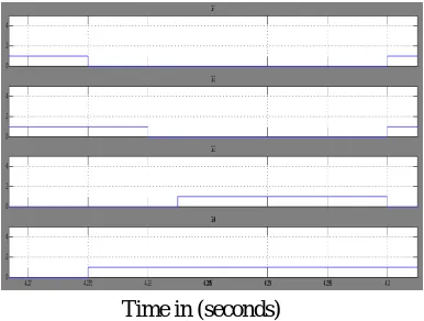
Typical converter waveforms are shown in fig 12,The gating signals for S2 and S3 are generated in such a way that both switches are each on for half a switching cycle, but are never on at the same time.
Time in (seconds) Fig.13. Generated pulses
PARAMETER VALUE
Lin Input inductor 4mH
C1,C2 Capacitor 2200μF
Lo Output inductor 10μH
Co Output
capacitor
The output voltage and current obtained is shown in fig 14, 285V dc is obtained at the output of the converter.
Time in (seconds) Fig.13. Output waveform
VI.CONCLUSION
A new single-stage ac-dc converter is presented in the paper. The converter performs input PFC and high dc output voltage. The active power factor correction method is used for the input side and obtain a power factor of 0.97. The outstanding feature of this converter is that it combines the performance of two-stage converters with the reduction of cost of single-stage converters. The paper explains its basic operating principles and modes of operation. Experimental results that confirm the feasibility of the converter are also presented in the paper.
REFERENCES
[1] Zhao, Q., Lee,F. C.,and Tsai, F., “Voltage and current stress reduction in single-stage power factor correction AC/DC converters with bulk capacitor voltage feedback,” IEEE Trans. Power Electron., vol. 17, no. 4, pp. 477–484, Jul. 2002.
[2] Moschopoulos, G., “A simple AC–DC PWM full-bridge converter withintegrated power-factor correction,” IEEE Trans. Ind. Electron., vol. 50,no. 6, pp. 1290–1297, Dec. 2003.
[3] Das, P., Li, S., and Moschopoulos, G., “An improved AC–DC single-stage full-bridge converter with reduced DC bus voltage “IEEE Trans. On Ind.Electron., vol.56, no. 12, pp. 4882 - 4893, 2009
[4] Ma, H., Ji Y., and Xu, Y., “Design and Analysis of Single-Stage Power Factor Correction Converter With a Feedback Winding,” IEEE Trans. Power Electronics, vol. 25, no. 6, pp. 1460-1470, jun. 2010.
[5] Wang,C.M., Lin, C.H., and Yang, T.C., “High-power-factor soft-switched DC power supply system,” IEEE Trans. Power Electron., vol. 26, no. 2, pp. 647–654, Feb. 2011.
[6] Agamy, M. S., and Jain, P. K., “An adaptive energy storage technique for efficiency improvement of single-stage three-level resonant AC/DC converters”, IEEE Trans. on Power Electron., vol. 47, no.1, pp. 176–184, Sep. 2011.