c e-ISSN: 2348-6848, p- ISSN: 2348-795X Volume 2, Issue 11, November 2015
International Journal of Research (IJR)
Available at http://internationaljournalofresearch.orgPerformance Analysis of Low Power Decoders Using
Reversible Computing
Manjinder Pal Singh
M.Tech, ECED, SVIETBanur, Punjab, India
Er. Birinderjit Singh
Assistant Professor, ECED, SVIETBanur, Punjab, India
Er.Amandeep Singh Bhandari
Assistant Professor, ECED, Punjabi University, Patiala, Punjab, India EMAIL: [email protected]
Abstract
In this paper performance analysis of 2:4 reversible decoder is proposed which can provide active high as well as active low outputs. The proposed decoder uses BVF gate, Double Feynman andFredkin gates and Trace circuit to get low power consumption and quantum cost. The proposed gate is fist extended to 4:16 decoder followed by an n-input decoder. The theoretical proposition is verified through Xilinx simulations. A comparison with existing reversible decoders is also included.
1. Introduction
A decoder, is a combinational circuit with (n) input line, and (2 ) output line. A decoder can n take the form of a multiple-input, multiple-output logic circuit that converts coded inputs into coded outputs, where the input and output codes are different. The output indicates presence or absence of specific number at the decoder input. To preserve the encoded information at the output in computational tasks pertaining to digital signal processing, communication, computer graphics, and cryptography applications [1].
The conventional computing circuits are irreversible i.e. the input bits are lost when the output is generated. This information loss during Computation culminates into increased power consumption [2]
According to R. Landauer‟s [3] research in the 1960s, the amount of energy (heat) dissipated for
every irreversible bit operation is given by KT ln2, where K is the Boltzmann‟s constant (1.3807×10 -23 JK -1) and T is the temperature at which computation performed. For T equal to room temperature (300 K), KT ln2 is approximately 2.8×10 -21 J, which is small but non-negligible. Bennett [4] showed that in order to avoid kTln2 joules of energy dissipation in a circuit it must be built from reversible circuits. In digital design, decoders find extensive usage to analyse data streams for a certain data code and give an output if the data is present like an address to a peripheral unit that needs
Service or in applications such as microprocessor memory system, microprocessor input-output system memory chip microprocessor instruction chip, also in Analog to Digital (ADC) and Digital to Analog Converters (DAC) which are used in some modification. Various different stages of a communication system. This paper therefore addresses the design of reversible decoders withsome modification.
1.1 Basic Concept of Reversible Logic
c e-ISSN: 2348-6848, p- ISSN: 2348-795X Volume 2, Issue 11, November 2015
International Journal of Research (IJR)
Available at http://internationaljournalofresearch.orginputs. On the other hand, the number of outputs introduced for maintaining reversibility is called garbage outputs. Some basic reversible gates most of the time being used are Peres Gate(PG), Toffoli Gate(TG), Fredkin Gate(FRG), Feynman Gate(FG),Modified Fredkin Gate(MFRG), BVF GATE, Double Feynman Gate(F2G) etc. From these gates MFRG and BVF gate are 4x4 gate, FG in 2x2 gate and other one are 3x3 gates. The cost of reversible gate is given in terms of number of primitive reversible gates needed to realize the circuit. [8]
a. Quantum Cost
Quantum Cost of the circuit is considered by knowing the number of simple reversible gates (gates of which rate is previously identified) needed to realize the circuit.
b. Garbage Output
The output of the reversible gate that is not used as a main output or as input to other gates is called the garbage output. In little the unexploited output of a reversible gate (or circuit) is the garbage output (s). These garbage outputs are required in the circuit to retain the reversibility concept. [10]
1.2 Organization of the work
This section describes the organization of the paper. Section 1 includes the introduction of reversibility. Section 2 shows the work done by the various researchers in the field of reversibility. Section 3 describes the concept of reversible logic gates. Section 4 includes the proposed work. Section 5 includes the conclusion and Section 6 includes result and Future work. References are shown next.
2. Literature Survey
The literature survey on reversible decoders shows that the focus is on either developing topology based on available reversible. In [5] the topology was based on only Fredkin gates with higher cost metrics whereas the one presented in [6] which has attractive cost metrics but it cannot
be extended further into a generalized n- input decoder. The reversible decoders in [5-6] provide only active high mode of operation. There is one introduced in [7] a reversible decoder which can provide both active high and active low mode of operation and utilizes Feynman and Fredkin gates it is also implemented using transmission gates. In [9] proposed a new method to reduce the quantum cost and power for various multiplexers using modified Fredkin gate. From this study another reversible decoder is introduces which also operate in active high and active low mode with using BVF, Double Feynman and Fredkin gates to reduce the power. The proposed topology is implemented using Xilinx 14.7 and verified.
3. Reversible Logic Gates
3.1. Feynman Gate
Feynman gate is a 2*2 one through reversible gate as shown in figure 1. The input vector is I(A, B) and the output vector is O(P, Q). The outputs are defined by P=A, Q= A⨁B. Quantum cost of a Feynman gate is 1. Feynman Gate (FG) can be used as a copying gate. Since a fan-out is not allowed in reversible logic, this gate is useful for duplication of the required
outputs.
Figure1- Feynman Gate
3.2. Double Feynman Gate (F2G)
c e-ISSN: 2348-6848, p- ISSN: 2348-795X Volume 2, Issue 11, November 2015
International Journal of Research (IJR)
Available at http://internationaljournalofresearch.orgFigure 2-Double Feynman Gate
3.3. Toffoli Gate
Figure 3 shows a 3*3 Toffoli gate. The input vector is I (A, B, C) and the output vector is O(P,Q,R). The outputs are defined by P=A, Q=B, R=AB⊕C.
Figure 3 -Toffoli Gate
3.4. Fredkin Gate (FRG)
Figure 4 shows a 3*3 Fredkin gate. The input vector is I (A, B, C) and the output vector is O (P, Q, R). The output is defined by P=A, Q=A'B
⨁ AC and R=A'C ⨁ AB.
Figure 4-Fredkin Gate
3.5. Reversible Peres Gate (PG)
The 3 × 3 (Peres, 1985) is designated as follows: Input vector Iv = (A, B, C) and output vectorOv = (P = A, Q = A⨁B, R = AB⨁C). Block diagram of Peres is showed in Figure 5 Peres gate is the combination of Feynman gate and Toffoli (1980) and this can contrivance operations like AND EX-OR.
Figure 5- Peres gate
3.6. Reversible BVF Gate
Figure 6 shows a 4 * 4 BVF gate [11]. This is a reversible double XOR gate and can be used for duplication of the required inputs to meet the fan-out requirements. The input vector is I(A,B,C,D) , the output vector is O(P,Q,R,S) and the output is defined by P = A, Q = A⊕B, R = C and S = C⊕D.
Figure 6-BVF Gate
4. PROPOSED WORK
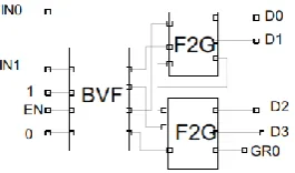
4.1. Proposed 2:4 Reversible Decoder
The proposed 2:4 Reversible decoder is
Figure 7- Proposed 2:4 Reversible Decoder shown in Figure.7. It uses one BVF gate and two Double Feynman gates (F2G). It has threeinputs
EN and IN
IN0, 1 where IN0andIN1are the
c e-ISSN: 2348-6848, p- ISSN: 2348-795X Volume 2, Issue 11, November 2015
International Journal of Research (IJR)
Available at http://internationaljournalofresearch.orgwill assume logic high. The proposed decoder uses three constant inputs and a two garbage output. Thus, the proposed circuit performs the operation in active high as well as active low mode in a very cost efficient manner. The next section describes the implementation of 3:8 decoder using decoder.
4.2. Proposed 3:8 Reversible Decoder
The block diagram of the proposed 3-to-8 decoder is shown in Figure 8, where
2 1
0,IN andIN
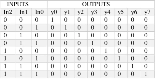
IN are the inputs to the decoder, EN is the enable line and Y (i = 0, 1 ...7) Represent the outputs. It uses the proposed 2-to-4 decoder and cascade it with Fredkin gate. It also uses an additional 1 to 5 tracer circuit in order to remove the fan out problem in the reversible decoder in case EN had been the output of any other reversible gate. This block copies input EN to 5 different lines and comprises of Double Feynman gates. Each of the tracer circuit output is applied to the input to the Fredkin gates. The tracer circuit, however, will not be needed if EN is the not an output of any other reversible gate. Table 1 and 2 show the truth tables of the proposed decoder with select line EN = 0 and 1 respectively. The next section describes the implementation of 4:16 decoder using decoder of Figure 10.
Figure 8- Proposed 3:8 Reversible Decoder The proposed 3:8 decoder can easily be extended to a generalized n× 2n reversible decoder where
n is greater than or equal to 3. The generalized decoder will use a 1 to (2n - 3) tracer circuit
which will copy the input S to each of the 2n –
3 lines and can easily be implemented by using Double Feynman gates in the same manner in which 1 to 5 tracer circuit was implemented. Table 1 Proposed 3:8 reversible Decoder with EN=0
INPUTS OUTPUTS
c e-ISSN: 2348-6848, p- ISSN: 2348-795X Volume 2, Issue 11, November 2015
International Journal of Research (IJR)
Available at http://internationaljournalofresearch.orgTable 2 Proposed 3:8 reversible Decoder with EN=1
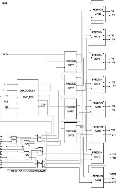
4.3. Proposed 4:16 Reversible Decoder
The proposed 4:16 Reversible decoder is shown in Figure 9. It uses Proposed 2:4 decoder and twelve Fredkin gates (FRG), and a one 1 to 13 Tracer circuit which used six Double Feynman gates. It has five inputs
EN and IN IN IN
IN0, 1, 2, 3 whereIN0,IN1, 3
2 andIN
IN are the inputs to the decoder and EN is the enable line which will enable the mode of operation for decoder and Y (i = 0, 1...15) Represent the outputs. The output lines of decoder are taken from the outputs of the eight cascaded Fredkin gates wherein each of the gates provides two of the sixteen outputs of the decoder. The active high outputs are achieved for EN=0, therefore only a single output will be at logic high and all other outputs will be at logic low. Conversely, EN=1 provides active low operation thus single output will be at logic low and all other outputs will assume logic high. The proposed decoder uses fifteen constant inputs and a three garbage output. Thus, the proposed circuit performs the operation in active high as well as active low mode in a very power efficient manner.
Figure.9-Proposed4:16 Reversible Decoder
5. Results and Discussions
5.1. 1:2 Decoder
Figure 10.Comparison of Power (W) vsVccint (V) of Existing and Proposed 1:2 Decoders
INPUTS OUTPUTS
In2 In1 In0 y0 y1 y2 y3 y4 y5 y6 y7
0 0 0 0 1 1 1 1 1 1 1
0 0 1 1 0 1 1 1 1 1 1
0 1 0 1 1 0 1 1 1 1 1
0 1 1 1 1 1 0 1 1 1 1
1 0 0 1 1 1 1 0 1 1 1
1 0 1 1 1 1 1 1 0 1 1
1 1 0 1 1 1 1 1 1 0 1
c e-ISSN: 2348-6848, p- ISSN: 2348-795X Volume 2, Issue 11, November 2015
International Journal of Research (IJR)
Available at http://internationaljournalofresearch.orgFigure 11. Power (W) vs Junction Temperature (C) of Existing and Proposed 1:2 Decoders
5.2. 2:4 Decoder
Figure 12. Power (W) vsVccint (V) of Existing andProposed 2:4 Decoders
Figure 13. Power (W) vs Junction Temperature (C) of Existing and Proposed 2:4 Decoders
5.3. 3:8 Decoder
Figure 14. Power (W) vsVccint (V) of Existing and Proposed 3:8 Decoders
Figure 15 Power (W) vs Junction Temperature (C) of Existing and Proposed 3:8 Decoders
5.4 4:16 Decoder
Figure 16. Power (W) vsVccint (V) of Existing andProposed 4:16 Decoders
c e-ISSN: 2348-6848, p- ISSN: 2348-795X Volume 2, Issue 11, November 2015
International Journal of Research (IJR)
Available at http://internationaljournalofresearch.orgTable 1. Comparison of Decoders
3:8 DECODER
Using FRG Gates(Existing)
36 12 2.523
Using, BVF F2G and FRG Gates(Proposed)
30 9 1.799
Proposed 4:16 DECODER
Using FRG Gates(Existing)
84 28 2.827
Using, BVF F2G and FRG Gates(Proposed)
78 21 1.919
Table 3 Comparison of proposed decoders with previous one
6. Conclusion
In this paper, we presented reversible decoders using BVF, F2G and FRG gates. Table 3 demonstrates that the proposed reversible decoders in terms of hardware complexity and quantum cost. Our proposed reversible decoders
with active low and active high mode using tracer circuit to avoid fan out, and can be applied to the design of complex systems in nanotechnology
Future Scope
This paper opens up some possible research directions which are described below:
Other combinational/sequential circuits such as multiplexers, encoders, shift registers, counters etc. can be optimized using various reversible logic gates having low power and quantum cost. Some other modifications can be done in this research work to reduce garbage output value and number of constant inputs/outputs and quantum cost as well with using other reversible gates such as Modified Fredkin gate, DPG or DKG gates.
The reversible logic circuits can also be designed with less area and delay.
References
[1] V. V. Shinde, A. K. Prasad, I. L. Markov, and J. P. Hayes, “Synthesis of Reversible Logic Circuits,” IEEE Tran Computer-aided Design of Int. Cir. And Syst., vol. 22, pp. 710-722, 2003 [2] Pandey, N., Dadhich, N., & Talha, M. Z. (2014, February). Realization of 2: 4 reversible decoder and its Applications. In Signal Processing and Integrated Networks (SPIN), 2014 International Conference on (pp. 349-353). IEEE.
[ 3] R. Landauer, ―Irreversibility and Heat Generation in the Computational Process‖, IBM Journal of Research and Development, 5, pp. 183-191, 1961.
[4] C.H. Bennett, “Logical Reversibility of Computation‖, IBM Research and Development”, pp. 525-532, November 1973.
[5] R. Aradhya, R, Chinmaye, and K. Muralidhara, “Design, Optimization and Synthesis of Efficient Reversible Logic Binary Decoder,” International Journal of Computer Applications, vol. 46, pp. 45-51, 2012.
Circuit Name Gate Used for Circuit Quant um Cost Gate Coun ts Power (W) 1:2 DECO DER Using FRG Gates(Exis ting)
5 1 4.394
Using F2G Gate(Prop
osed)
2 1 2.682
2:4 DECO DER Using FRG Gates(Exis ting)
12 4 4.999
Using BVF F2G
and FRG Gates(Pro posed)
c e-ISSN: 2348-6848, p- ISSN: 2348-795X Volume 2, Issue 11, November 2015
International Journal of Research (IJR)
Available at http://internationaljournalofresearch.org[6] M. Nachtigal, and N. Ranganathan, “Design and Analysis of a
Novel Reversible Encoder/Decoder”, 2011 11th IEEE International Conference on Nanotechno'logy, Portland Marriott, pp. 1543-1546, 2011.
[7] Pandey, N., Dadhich, N., & Talha, M. Z. (2014, February). Realization of 2: 4 reversible decoder and its Applications. In Signal Processing and Integrated Networks (SPIN), 2014 International Conference on (pp. 349-353). IEEE.
[8] Thapliyal, Himanshu, and
NagarajanRanganathan. "Design of reversible sequential circuits optimizing quantum cost, delay, and garbage outputs." ACM Journal on Emerging Technologies in Computing Systems
(JETC) 6, no. 4 (2010): 14.
[9] Malhotra, Ashima, Charanjit Singh, and Amandeep Singh, “Efficient Design of Reversible Multiplexers with Low Quantum Cost and Power Consumption”, International Journal of Emerging Technology and Advanced Engineering, Volume 4, Issue 7, July 2014, pp. 518*523
[10] Robert Wille, Rolf Drechsler, “Towards a Design Flow for Reversible Logic”, Springer, 2010.
[11] Bhagyalakshmi, H R and Venkatesha, M K, “An improved design of a multiplier using reversible logic gates.” International Journal of Engineering Science and Technology,Vol. 2(8), 2010, 3838-3845.
[12] Santosh Rani and Amandeep Singh Bhandari, “A Survey on Reversible Logic Gates”, International Journal of Computer Applications (0975 – 8887), pp. 1-3.
[13] Ashima Malhotra, Charanjit Singh, Amandeep Singh, “Efficient Design of Reversible Multiplexers with Low Quantum Cost”, Int. Journal of Engineering Research and Applications, Vol. 4, Issue 7( Version 4), July 2014, pp.20-23.
[14] Sukhjeet Kaur and Amandeep Singh Bhandari, “Design and Performance Analysis of Encoders using Reversible logic gates”,