ISSN (Print) : 2320 – 3765 ISSN (Online): 2278 – 8875
I
nternational
J
ournal of
A
dvanced
R
esearch in
E
lectrical,
E
lectronics and
I
nstrumentation
E
ngineering
(A High Impact Factor & UGC Approved Journal)
Website: www.ijareeie.com
Vol. 6, Issue 9, September 2017
An Over-modulation Algorithm for Carrier
Based Space Vector PWM Inverters
A.N.Maheswarappa1,Dr. Sanjay Lakshminarayanan2
Professor, Dept. of EEE Global Academy of Technology, Bangalore, India1
Associate Professor, Dept. of EEE, M.S.Ramaiah University of Applied Sciences, Bangalore, India2
ABSTRACT: Carrier based Space Vector Pulse Width Modulation (SVPWM) has the advantage of ease of implementation and lower processor overheads as no timing calculation is required. Appropriate reference signals are generated, which, on comparison with a triangular carrier, gives the gating pulses for the semiconductor switches. However, just as in the case of switching time calculation, the amplitude of the reference waveform does not bear a linear relationship to the output fundamental voltage in the over-modulation region. This paper discusses a method to generate a modified reference signal so that a linear relationship exists between the commanded modulation index and the actual fundamental output over the entire range of modulation index.
KEYWORDS :Linear modulation, Carrier based SVPWM, Reference pre-processor, Modified look-up-table.
I. INTRODUCTION
The output fundamental voltage has to be varied in inverter fed AC drive systems depending on the speed requirements. This is facilitated by varying the modulation index of the inverter based on the control algorithm. The modulation index can be varied from the lowest value to that value of fundamental voltage available in the six-step operation mode. It is desirable to have a linear relationship between the modulation index and the fundamental component of output voltage. The modulation index determines the switching times for the different inverter states in conventional space vector modulation, and the magnitude of the reference voltage in carrier based PWM techniques. The fundamental component of the inverter output voltage is directly proportional to the modulation index, in either case, only in the linear modulation range. Beyond the linear range, increasing modulation index does not proportionately increase the output fundamental component. The exact relation between fundamental and the amplitude of the reference also depends on the ratio of carrier to fundamental frequencies in carrier based schemes. If the carrier is of sufficiently high frequency, then it can be assumed that the output voltage and reference signal are directly related. In this paper, carrier based implementation is discussed, for both sinusoidal pulse width modulation (SPWM) and conventional space vector pulse with modulation (CSVPWM).
II. MODULATION ALGORITHMS
The fundamental component of the output voltage of an inverter can be controlled in carrier based algorithms by varying the magnitude of the reference signal vis-a-vis the fixed amplitude carrier signal. A figure of quantifying the output is the modulation index (MI). The modulation index has been variously defined as the ratio of the normalized fundamental output voltage to the normalized fundamental output voltage in six step operation (M I ≤ 1), and the ratio of the peak of the reference signal to the peak of the carrier. In this paper, the modulation index is taken as the ratio of normalized fundamental output voltage to peak of carrier. The normalized fundamental output voltage is the
ratio of output fundamental to half the DC link voltage. The maximum MI is then
π 4
ISSN (Print) : 2320 – 3765 ISSN (Online): 2278 – 8875
I
nternational
J
ournal of
A
dvanced
R
esearch in
E
lectrical,
E
lectronics and
I
nstrumentation
E
ngineering
(A High Impact Factor & UGC Approved Journal)
Website: www.ijareeie.com
Vol. 6, Issue 9, September 2017
or gain for different modulation schemes has be performed in [3]. The operation of the inverter under continuous linear mode has been described in [4]. A Fourier analysis of SVM inverters in the over-modulation range has been described in [5]. An implementation of the SVPWM is described in [6] where modified timings are used, an equivalent implementation of conventional SVPWM based on carrier comparison is dis- cussed in [7]. Relationship Between Space-Vector Modulation and Three-Phase Carrier-Based PWM[8]. Different algorithms are also discussed for multi-level inverters where several topologies are discussed, using three-phase reference signals and multi-level-shifted carriers of various dispositions.[9], [10].
This paper analyses the fundamental component of the output for both SPWM and SVPWM in the time domain by evaluating the relevant Fourier component of the reference signal whose amplitude is between the positive and negative peaks of the reference signal. The paper then suggests a modification of the reference so that a linear relationship exists between the commanded modulation index and the fundamental component of the output voltage.
III. SINUSOIDAL PULSE WIDTH MODULATION
In sinusoidal pulse width modulation (SPWM), a carrier of switching frequency is compared with a sinusoidal reference signal to generate the gating pulses. The normalized carrier is assumed to vary over a magnitude of unity in both positive and negative direction. The average output pole voltage of the inverter depends on the peak amplitude of the modulating and carrier signals. For peak of modulating signal less than unity, the output pole voltage is proportional to the peak of modulating signal and the DC link voltage. The modulation index is defined as the ratio of the peak fundamental output voltage V1 to the peak fundamental output when the amplitude of reference is equal to the
amplitude of the carrier. In the linear modulation region, the peak amplitude Vm of the reference is less than unity. If
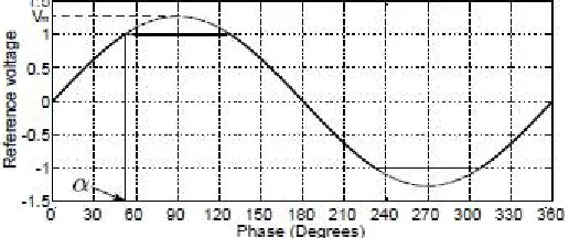
the magnitude of the reference voltage exceeds unity, that part of the reference above unit magnitude does not result in the generation of any switching pulses. The peak amplitude of the reference effectively is then unity, which is also the peak of the carrier. This means that all values of reference above unit magnitude is clipped as in Fig.1. The figure also indicates a phase angle α at which a reference in the over-modulation region crosses unity. Although the reference has a peak amplitude of Vm , the output fundamental will be lower than this value because of the clipping. The peak of
the output fundamental can be determined by determining the Fourier coefficient of the fundamental component of the clipped reference.
Fig. 1: Limiting of reference voltage in over-modulation region
In the over-modulation region therefore, the modulating signal can be defined as:
V
m
t
t
t
t
f
sin
,
0
2
,
1
(1)
ISSN (Print) : 2320 – 3765 ISSN (Online): 2278 – 8875
I
nternational
J
ournal of
A
dvanced
R
esearch in
E
lectrical,
E
lectronics and
I
nstrumentation
E
ngineering
(A High Impact Factor & UGC Approved Journal)
Website: www.ijareeie.com
Vol. 6, Issue 9, September 2017
02 2
1
sin
sin
4
t
d
t
t
d
t
V
V
m (2)
4
cos
2
sin
2
4
m
V
(3)The value of α can be determined from the reference voltagewaveform as Vmsinα = 1. Substituting for Vm in the above
equation, the magnitude of the fundamental component can be expressed as:
sin
cos
2
1
V
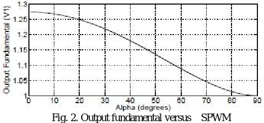
(4)The maximum value of fundamental occurs at α = 0 for which equivalently, the modulation index become the theoretical maximumof
4
realizing that the first term in the braces is the sinc function. A plot of the variation of the
fundamental with the angle α is shown in Fig.2.
Although determining the value of α to determine peak of reference voltage requires solving the transcendental equation, alternate ways of implementation are possible. Since modern day processors are extremely fast, a comparison operation can be performed to determine the value of intersection angle for a given fundamental voltage required. The angle is ramped up from zero in increments. On a match of the function with the desired fundamental value, the value of alpha is the angle at which the match occurred. The required reference voltage peak amplitude is then determined by evaluating the sine and cosine of this intersection angle from a sine look-up-table. The search algorithm can be optimized further since the value of the function is monotonic with respect to the intersection angle.
Fig. 2. Output fundamental versus _ SPWM
ISSN (Print) : 2320 – 3765 ISSN (Online): 2278 – 8875
I
nternational
J
ournal of
A
dvanced
R
esearch in
E
lectrical,
E
lectronics and
I
nstrumentation
E
ngineering
(A High Impact Factor & UGC Approved Journal)
Website: www.ijareeie.com
Vol. 6, Issue 9, September 2017
Fig. 3. Peak reference fundamental versus peak output fundamental
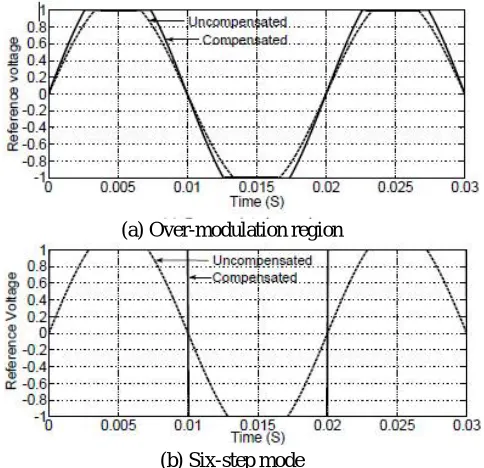
The reference fundamental thus has to be corrected in the over-modulation region to compensate for the loss of output fundamental because of the reference being clipped to the peak of the carrier. Fig.4 shows the compensated and uncompensated reference voltage wave-forms for two different values of modulation index.
IV. SPACE VECTOR PULSE WIDTH MODULATION
SVPWM increases the range of linear modulation by adding a common mode to the three phase reference signals. This is facilitated by altering the switching times so that the effective time is positioned in the middle of the switching period or by a carrier based PWM scheme wherein a common mode voltage signal is added to the reference signals of the three phases. Effectively, the two zero states are applied for equal duration in either case.
(a) Over-modulation region
(b) Six-step mode
Fig. 4. Compensated and Uncompensated reference signals (SPWM)
The three phase reference voltages can be re-designated as Vmax, Vmid and Vmin depending on their instantaneous values.
Then, for equal zero state times at any instant, a common voltage is added to all three phase reference signals and the following equation must be satisfied:
2
1
ISSN (Print) : 2320 – 3765 ISSN (Online): 2278 – 8875
I
nternational
J
ournal of
A
dvanced
R
esearch in
E
lectrical,
E
lectronics and
I
nstrumentation
E
ngineering
(A High Impact Factor & UGC Approved Journal)
Website: www.ijareeie.com
Vol. 6, Issue 9, September 2017
For
6
0tmiddle valued signal is that of the ’a’ phase and adding half of this to the same phase signal gives the’a’ phase reference signal for this interval. For
2 6
t the middle valued signal is that of the 'c' phase and so thereference
signal is sum of the ’a’ phase signal and the ’c’ phase signal. The function can thus be defined as:
6
0
sin
2
3
2
6
cos
4
3
sin
4
3
t
t
m
V
t
t
m
V
t
m
V
(5)
This modulating signal is compared with a triangular carrier whose normalized amplitude can be considered to be unity as in the case of the sinusoidal pulse width modulation. The reference signal so generated has a common mode component present in the phase voltages, but do not appear in the line to line voltages. Using this reference instead of a sinusoidal signal also increases the range of linear modulation compared to the sinusoidal PWM. This is because the peak amplitude of the reference has been reduced with the addition of the common mode, thereby giving the option of further increasing the fundamental component before over-modulation begins.
Fig. 5. Fundamental and modified with common mode
phase angleat peak of reference and maximum linear modulation: The reference signal generated in Eq. 5 is plotted in Fig.5 with the fundamental also shown. The second term in the above equation has a higher magnitude than the first, and the maximum value of the reference can be determined by differentiating the above with respect to ωtand equating
to zero. The phase angle then turns out to be
3
and the maximum value of fundamental when the magnitude of the
reference signal is unity at an angle of
3
t is
3 2
Thus it can be seen that by employing SVPWM, the range of linear
modulation has increased by around 15% compared to the sinusoidal PWM whose peak phase fundamental is unity.
Symmetry about 3
: The second term in the above function represents the modulating signal for 6 2
t . This termcan be
shown to be symmetric about
3
t by evaluating it for
3
t and
3
t , α representing a shift to either side as
depicted in Fig.6. The term evaluates to the same in either case, proving the symmetry.
A. Regions of modulation
Depending on the modulation index, the modulation can be categorized into three distinct regions.
Linear modulation: For
3
2
m
the inverter is operating in the linear modulation region, and the fundamental outputISSN (Print) : 2320 – 3765 ISSN (Online): 2278 – 8875
I
nternational
J
ournal of
A
dvanced
R
esearch in
E
lectrical,
E
lectronics and
I
nstrumentation
E
ngineering
(A High Impact Factor & UGC Approved Journal)
Website: www.ijareeie.com
Vol. 6, Issue 9, September 2017
Over-modulation region 1: As the amplitude of the reference is further increased
3 2
m the modulation is nonlinear.
Fig. 6. Clipped reference signal and angle α in over-modulation region 1
The fundamental output of the inverter is less than the fundamental component of the modulating signal, and this is evident in the clipping of the reference at the extreme values where the reference exceeds ±1 as can be seen in Fig.6. This over-modulation region can be subdivided into two regions. The first region corresponds to that range of modulation index for which the reference is cut twice by the extreme of the carrier. The magnitude of fundamental output has to be determined by evaluating the Fourier coefficient of the fundamental. The output waveform can be defined in this region as
6
0
sin
2
3
6
cos
4
3
sin
4
3
3
2
1
2
3
2
cos
4
3
sin
4
3
t
t
m
V
t
t
m
V
t
m
V
t
t
t
m
V
t
m
V
(6)The fundamental output voltage can be found by taking the Fourier component of the fundamental (n=1) of the above describing function. The integration can be done over quarter cycle and the multiplied by
4
as before. Integrating over
the different intervals. During the first interval, the relevant integral becomes
6 0 28
3
12
2
3
sin
2
3
m mV
t
d
t
V
The relevant integral of the function during the second interval is
2
cos
4
1
8
1
4
3
8
3
2
sin
4
1
12
2
4
3
sin
cos
4
3
sin
4
3
6 m m m mV
V
t
d
t
t
V
t
V
The integral over the third interval reduces to
3 2sin
2
3
cos
2
3
sin
t
d
t
ISSN (Print) : 2320 – 3765 ISSN (Online): 2278 – 8875
I
nternational
J
ournal of
A
dvanced
R
esearch in
E
lectrical,
E
lectronics and
I
nstrumentation
E
ngineering
(A High Impact Factor & UGC Approved Journal)
Website: www.ijareeie.com
Vol. 6, Issue 9, September 2017
2
sin
8
3
2
cos
8
1
4
1
4
3
...
...
2
sin
8
1
2
cos
8
3
12
2
4
3
sin
cos
4
3
sin
4
3
2 3 2 m m m mV
V
t
d
t
t
V
t
V
Summing up the different regions and multiplying by
4
, the magnitude of the output fundamental becomes
2
sin
3
cos
2
3
2
sin
4
1
2
cos
4
3
4
3
4
V
m(7)
Increasing the modulation index further results in the value of α reducing further, till, at one instant, the value of α becoming exactly
6
. This point defines the end of OMR1 and the beginning of OMR2. The defining function from this
point onward changes. The magnitude of the fundamental output at this transition region can be obtained by
substituting the value of α in either Eq.7 or Eq.12. The output fundamental (and the MI) evaluates to
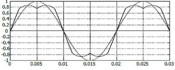
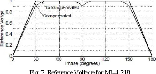
1.218 4 3 6 4 Fig.7shows an uncompensated reference of peak amplitude 1.218 and a compensated reference where the peak has been
increased to
3
4
The mapping on the voltage space vector plane is shown in Fig.8(a).
Fig. 7. Reference Voltage for MI=1.218
Over-modulation region 2: Increasing the modulation index further results in the vector being ’held’ in one of the active states as there is an interval where both the extreme valued reference signals and the middle valued signal are at one or the other extremities for some duration of time.
ISSN (Print) : 2320 – 3765 ISSN (Online): 2278 – 8875
I
nternational
J
ournal of
A
dvanced
R
esearch in
E
lectrical,
E
lectronics and
I
nstrumentation
E
ngineering
(A High Impact Factor & UGC Approved Journal)
Website: www.ijareeie.com
Vol. 6, Issue 9, September 2017
This implies that a state is applied for several carrier cycles before it shifts to another state. Another important aspect is that there is no zero state being applied, as, the maximum and minimum valued signals are always at one of the opposite extremes. On the space vector plane, the trajectory this region of operation will be along the boundary of the hexagon as shown in Fig. 8(b). The fundamental component can be evaluated using the Fourier series as before, the function being defined by:
t
t
m
V
t
ref
0
sin
2
3
2
1
(8)
Evaluating the Fourier series of the above waveform for magnitude of the fundamental component yields
02 2
1
sin
sin
2
3
4
t
d
t
t
d
t
V
V
m (9)
4
cos
2
sin
2
2
3
4
m
V
(10)The value of α can be determined from the intended voltage waveform as.
sin
1
2
3
mV
(11)Substituting for Vm in the above equation, the magnitude of the fundamental component can be expressed as:
sin
cos
2
1
V
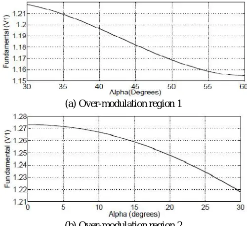
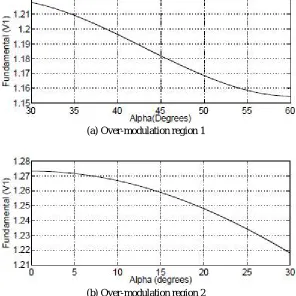
(12)Fig.9(a) and (b) show the plots of variation of fundamental versus the angle alpha in over-modulation regions 1 and 2. The peak of the reference required for linear output of fundamental versus the output fundamental is shown in Fig.10 (a) and (b)
(a) Over-modulation region 1
(b) Over-modulation region 2
ISSN (Print) : 2320 – 3765 ISSN (Online): 2278 – 8875
I
nternational
J
ournal of
A
dvanced
R
esearch in
E
lectrical,
E
lectronics and
I
nstrumentation
E
ngineering
(A High Impact Factor & UGC Approved Journal)
Website: www.ijareeie.com
Vol. 6, Issue 9, September 2017
B. Time domain wave-forms in SVPWM
The wave-forms of the reference signals for the three phases in the three regions of modulation has the added advantage of providing information on the time duration for which the different states are applied. While the vector represented in the space phasorplane rotates with uniform angular velocity ofωt radians per second in the linear and over-modulation region 1, the vector is held for some time at one of the six active states in over-modulation region 2.
(a) Over-modulation region 1
(b) Over-modulation region 2
Fig. 10. Peak phase reference versus peak output fundamental
The duration for which the vector is held at one of the active states depends on the modulation index, and will vary from zero at the beginning of region 2 to 60 degrees of phase angle equivalent in the six-step mode of operation. This holding duration cannot be represented in the space phasor plane as no information of time is available. However, the time domain wave forms will clearly indicate the duration for which the vectors are applied as seen in Fig.11.
V. RESULTS A. Waveform generation
ISSN (Print) : 2320 – 3765 ISSN (Online): 2278 – 8875
I
nternational
J
ournal of
A
dvanced
R
esearch in
E
lectrical,
E
lectronics and
I
nstrumentation
E
ngineering
(A High Impact Factor & UGC Approved Journal)
Website: www.ijareeie.com
Vol. 6, Issue 9, September 2017
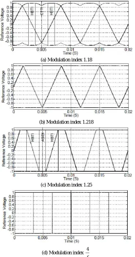
valued phases are always at unit magnitude, positive and negative. The middle valued phase switches, thereby applying adjacent active states. This interval on the time axis is indicated as Hexagonal Boundary Transit Interval (HBTI). At the end of OMR1 (modulation index 1.218), the locus of the vector is entirely along the hexagon boundary as the magnitude of the maximum and minimum reference phase signals are ±1. This mode is indicated in Fig.11 (b)
(a) Modulation index 1.18
(b) Modulation index 1.218
(c) Modulation index 1.25
(d) Modulation index
4
ISSN (Print) : 2320 – 3765 ISSN (Online): 2278 – 8875
I
nternational
J
ournal of
A
dvanced
R
esearch in
E
lectrical,
E
lectronics and
I
nstrumentation
E
ngineering
(A High Impact Factor & UGC Approved Journal)
Website: www.ijareeie.com
Vol. 6, Issue 9, September 2017
As the reference is further increased, there exists an interval where an active vector is applied or ’held’ for a certain interval before the HBTI. This interval is indicated as Active State Dwell Interval (ASDI) where-in all the three references are of unit positive or negative magnitude, and there is no middle valued phase that switches states in a carrier cycle. The average voltage vector applied over one switching cycle is one of the six active states and a zero state is not applied in this mode. This happens in OMR2 where a greater value of output fundamental is desired. Since the total time interval over a cycle remains fixed, the holding of an active state reduces the HBTI and this can be seen in Fig.11(c). This effect cannot be depicted on the space vector locus diagram as time information is not shown. As the modulation index is further increased, the ASDI increases at the expense of HBTI till, in the six step mode of operation, active states are applied for 60 degrees each giving the maximum possible fundamental output. This mode is depicted in Fig.11(d)
B. Algorithm implementation
The algorithm described was implemented in generating the reference voltages in an open loop v/f control of an induction motor drive in order to verify its compatibility with the existing control scheme. A representative soft start implementation was utilized, and the output voltage generated for step change in speed reference as well as for reversal. It can be seen that for a step change in speed command to the maximum commanded speed, the reference smoothly transits to a square wave as expected. This transition is shown in Fig 11.
Fig. 12. Change in speed reference to maximum speed
The wave-forms for speed reversal in Fig.12 show the effect of the soft start circuit in preventing any sudden change in reference voltages.
Fig. 13. Speed reversal
VI. CONCLUSIONS
ISSN (Print) : 2320 – 3765 ISSN (Online): 2278 – 8875
I
nternational
J
ournal of
A
dvanced
R
esearch in
E
lectrical,
E
lectronics and
I
nstrumentation
E
ngineering
(A High Impact Factor & UGC Approved Journal)
Website: www.ijareeie.com
Vol. 6, Issue 9, September 2017
employed for volts/hertz control as well as vector control of induction motorswhere the instantaneous values of reference signals are used to generate the switching states. It is applicable for both two level and also multi-level inverters. The implementation is easier than calculation of state timings since the need for evaluating operation in over-modulation region and subsequent recalculation of switching times can be avoided in this scheme.
REFERENCES
[1]. J. Holtz, “Pulsewidth modulation-a survey,” IEEE Trans. Ind Electron., vol. 39, no. 5, pp. 410–420, Dec 1992.
[2]. D. C. Lee and G. M. Lee, “A novel over-modulation technique for spacevector pwm inverters,” IEEE Trans. Power Electron., vol. 13, no. 6,
Nov 1998.
[3]. M. Hava, R. J. Kerkman, and T. A. Lipo, “Carrier-based pwmvsi over-modulation strategies: Analysis, comparison, and design,” IEEE Trans.
Power Electron., vol. 13, no. 4, pp. 674–689, Jul 1998.
[4]. J. Holtz, W. Lotzkat, and A. Khambadkone, “On continuous control of p w m inverters in over-modulation range including six-step mode,”
IEEE Trans. Power Electron., vol. 8, no. 4, pp. 546–553, 1993.
[5]. S. Bolognani and M. Zigliotto, “Space vector fourier analysis of svm inverters in the over-modulation range,” Proc. PEDES, pp. 319–324.,
1996.
[6]. D.-W. Chung, J.-S. Kim, and S.-K. Sul, “Unified voltage modulation technique for real-time three-phase power conversion,” IEEE Trans. Ind.
Appl., vol. 34, no. 2, Mar/Apr 1998.
[7]. P. S. Varma and G. Narayanan, “Space vector pwm as a modified form of sine-triangle pwm for simple analog or digital implementation,”
IETE Journal of Research, vol. 52, no. 6, pp. 435–449, 2006.
[8]. K. Zhou and D. Wang, “Relationship between space-vector modulation and three-phase carrier-based pwm: A comprehensive analysis,” IEEE
Trans. Ind. Electron., vol. 49, no. 1, p. 186, Feb 2002.
[9]. L. M. Tolbert and T. G. Habetler, “Novel multilevel inverter carrier-based pwm method,” IEEE Trans. Ind. Appl., vol. 35, no. 5, pp. 1098–
1106, Sep/Oct 1999.
[10]. J. Rodríguez, J.-S. Lai, and F. Z. Peng, “Multilevel inverters: A survey of topologies, controls, and applications,” IEEE Trans. Ind. Electron.,