Implementation of BCD Adder using Clockgating
N Vinod Kumar1, K Prasad babu2 and V Sundara Siva Kumar3
1
ECE, JNTUA/Dr KVSubbaReddyCollege of Engineering for Women/, Kurnool, AndhraPradesh 518218, India
2
ECE, JNTUA/ Dr KVSubbaReddyCollege of Engineering for Women /, Kurnool, AndhraPradesh 518218, India
3
ECE, JNTUA/ Dr KVSubbaReddyCollege of Engineering for Women /, Kurnool, AndhraPradesh 518218, India
Abstract
There is a growing importance of decimal arithmetic in commercial, financial and internet based applications. These applications cannot tolerate errors that result from the conversion of binary format to decimal format. Thus, hardware support for decimal arithmetic is receiving considerable attention.BCD adder are used for such applications. Clock gating is a power reduction technique that has been used successfully in the custom ASIC domain. Clock and logic signal power are saved by temporarily disabling the clock signal on registers whose outputs do not affect circuit outputs. Clock gating is a way of reducing switching activity on circuit signals, and it entails temporarily disabling the clocking of specific registers when the outputs of those registers are inconsequential to circuit outputs. In this paper implementation of BCD adder using VHDL is done. Clock Gating technique is applied to the designed BCD adder, Comparison of power dissipated with and without clock gating is done. Dynamic Power, Static power are affected in this design. VHDL language is used to implement the BCD adder.Mimas V2 Spartan 6 FPGA Development Board is used.
Keywords: BCD Adder, Power Dissipation, ClockGating,VHDL.
1. Introduction
In digital design, One of the important issue for VLSI designers is Power consumption. For battery-operated systems, such as laptops, calculators, cell phones and MP3 players power dissipation is critical since it determines the battery life and has a direct impact on the consumer valuation of the product. Obtaining Low power consumption is primary requirement in todays design. Power consumption in CMOS circuits can be divided in two components, Static dissipation, which is due to leakage current. Leakage current is a small current that flows through the transistor even when the transistor is off and there is no switching activity. Dynamic dissipation, which is due to charging and discharging of load capacitances and short circuit currents while both pMOs and nMOS networks are partially on. Total Power, Dynamic power, Static Power are given by
Ptotal=PDynamic+PStatic---(1) PDynamic=1/2 αCfV2---(2) where C is Load Capacitance, f is frequency,
Supply Voltage. α is activity factor. Pstatic= VccIcc--- (3)
With BCD Adder Decimal addition is possible. The decimal sum of the addend and augend, and a carry that is generated if the sum exceeds a decimal value of 9 is produced. As the IEEE standard for decimal floating point is approved, hardware support for decimal floating point arithmetic will be incorporated in processors for various applications. Still, a major consideration while implementing Binary Coded Decimal (BCD) arithmetic is to enhance its speed as much as possible. BCD is a decimal representation of a number directly coded in binary, digit by digit. For example, the number (9527)10 is
www.ijiset.com
2. Clock Gating
Gate based clock gating are of two types AND, NOR based. The AND gate is the most common gate used for clock gating because of its simple logic. To gate the clock, a two input AND gate is inserted in the four bit counter having one of its input as clock and other as the enable signal “En”. When enable signal is equal to zero and the clock can take any value (i.e. it can either be in positive or negative cycle). The output of the AND gate which is also known as the gated clock “GCLK = 0”. When enable is equal to one then the output of the gated clock (GCLK) varies according to the clock signal. When output of the gated clock (GCLK) undergoes a transition from high to low (i.e. when the negative edge occurs), the counter gets incremented. The drawback in this technique is that, for the positive edge triggered counter when enable signal goes from 1 to 0 and when the clock is at rising edge, a glitch occurs because of the greater falling time period of enable signal. The output obtained is incorrect, because of the aforementioned reason. Any hazard that occurs when enable is equal to one is directly imprinted on to the GCLK this is an unstable behavior of the circuit. The NOR gate gives output of the gated clock (GCLK) equal to one only when both enable and the clock have a value zero. Hence the enable signal is passed through a NOT gate before being fed as one of the inputs of the NOR gate so that the output of the gated clock (GCLK) is obtained when enable is ON. NOR gate clock gating is used in particular for positive edge triggered circuits.
3. Implementation
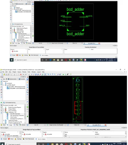
Fig. 1. Schematic view of BCD adder
www.ijiset.com
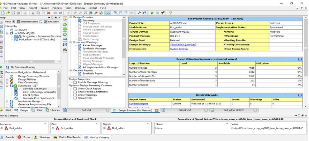
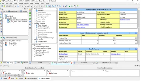
Fig. 4. Device Utilization of 4 bit BCD adder
In the device utilization summary of 4-bit BCD adder, no of IOB’s, is 6% , when compared with nonclockgating BCD adder.
4. Conclusions
www.ijiset.com
With Clock gating results are
From the above results it is clear that the BCD adder with Clock gating is dissipating less power when compared with normal clock. The total power which is a combination of static and dynamic power is affected with 3.189 %. Therefore we can conclude that dynamic power is affected by clock gating technique. Future work will involve incorporating the clock gating aware placement algorithm into a complete aware FPGA CAD flow, allowing trade-offs between other power-aware tool phases to be explored. Another future direction involves modeling clock gating within the VPR router to permit extraction of accurate post-routing critical path delay and interconnect capacitance. It will also be important to understand the impact of gating on timing analysis to ensure functional correctness is maintained when enable signals are migrated from flip-flops to enable pins on clock network switches.
References
[1] V. G. Oklobdzija, Digital System Clocking-High Performance and Low-Power Aspects. New York, NY, USA: Wiley, 2003. [2] Frank Emnett and Mark Biegel "Power reduction through RTL clock gating," Automotive Integrate Electronics Corporation, SNUG San Jose, 2000.
[3] L. Benini, A Bogliolo, G. De Micheli, "A survey of design techniques for system-level dynamic power management," IEEE Transactions on Very Large Scale Integration (VLSI) Systems, vol.8, no.3, pp.299-316, June 2000.
[4] Hosny M. S. , Yuejian Wu, "Low power clocking strategies in deep submicron technologies," IEEE International Conference on Integrated Circuit Design and Technology and Tutorial, ICICDT 2008, pp.143-146, 2-4 June 2008.
[5] Bhutada R. , Manoli Y. , "Complex clock gating with integrated clock gating logic cell," International Conference on Design & Technology of Integrated Systems in Nanoscale Era, DTlS 2007, pp.164-169, 2-5 Sept. 2007.
[6] Kathuria, Jagrit, M. Ayoubkhan, and Arti Noor, "A Review of Clock Gating Techniques." MIT International Journal of Electronics and Communication Engineering vol. I, no. 2, pp.106-114, 2011.
[7] Wimer S. , Koren I. , "Design Flow for Flip-Flop Grouping in Data-Driven Clock Gating," IEEE Transactions on Very Large Scale Integration (VLSI) Systems, vo1.22, no.4, pp.771-778, April 2014.
[8] Chunhong Chen, Kang c., Sarrafzadeh M. , "Activitysensitive clock tree construction for low power," Proceedings of the International Symposium on Low Power Electronics and Design, ISLPED '02., pp.279-282, 2002.
[9] Farrahi AH. , Chunhong Chen, Srivastava A, Tellez G., Sarrafzadeh, "Activity-driven clock design," IEEE Transactions on Computer-Aided Design of Integrated Circuits and Systems, vo1.20, no.6, pp.705-714, June 2001.
[10] Shinde .T., Salankar S. S., "Clock gating - A power optlmlzmg technique for VLSI circuits," Annual IEEE Conference INDICON, pp.I-4, 16-18 Dec. 2011.
[11] Pandey B. , Singh D., Baghel D., Yadav J. , Pattanaik M., "Clock Gated Low Power Memory Implementation on Virtex-6 FPGA," 5th International Conference Computational Intelligence and Communication Networks (CICN), pp. 409-412, 27-29 Sept. 2013. [12] Pedroni, Volnei A, "Circuit Design and simulation with VHDL", 2nd Edition, MIT Press, Year 2011.
First Author Mr N Vinod kumar Assistant Professor,Dept of ECE, DrKVSW,JNTUA, Kurnool, AP,India. He has around 4 years of experience. His areas of interests are VLSI, Embedded.
Second Author Mr K.PrasadBabu, Associate Professor,Dept of ECE, DrKVSW,JNTUA, Kurnool, AP,India. He has around 14 years of experience. He worked as Intern at DRDO Hyderabad. His areas of interests are VLSI,Embedded,Image Processing.