Accelerating Fully Homomorphic Encryption over the
Integers with Super-size Hardware Multiplier and
Modular Reduction
Xiaolin Cao, Ciara Moore, Maire O’Neill, Elizabeth O’Sullivan and Neil Hanley CSIT, ECIT, Queen’s University Belfast, Belfast, Northern Ireland, UK
[email protected], [email protected], [email protected], [email protected], [email protected]
Abstract. A fully homomorphic encryption (FHE) scheme is envisioned as be-ing a key cryptographic tool in buildbe-ing a secure and reliable cloud computbe-ing environment, as it allows arbitrarily evaluation of a ciphertext without revealing the plaintext. However, existing FHE implementations remain impractical due to their very high time and resource costs. Of the proposed schemes that can perform FHE to date, a scheme known as FHE over the integers has the ad-vantage of comparatively simpler theory, as well as the employment of a much shorter public key making its implementation somewhat more practical than other competing schemes.
To the author’s knowledge, this paper presents the first hardware implemen-tations of encryption primitives for FHE over the integers using FPGA technol-ogy. First of all, a super-size hardware multiplier architecture utilising the Inte-ger-FFT multiplication algorithm is proposed, and a super-size hardware Barrett modular reduction module is designed incorporating the proposed multiplier. Next, two encryption primitives that are used in two schemes of FHE over the integers are designed employing the proposed super-size multiplier and modular reduction modules. Finally, the proposed designs are implemented and verified on the Xilinx Virtex-7 FPGA platform. Experimental results show that the speed improvement factors of up to 44.72 and 54.42 are available for the two FHE encryption schemes implemented in FPGA when compared to the corre-sponding software implementations. Meanwhile, the performance analysis shows that further improvement is speed of these FHE encryption primitives may still be possible.
Keywords: Barrett Modular Reduction, Fully Homomorphic Encryption, FPGA, Hardware, Integer-FFT Multiplication.
1
Introduction
security technologies and privacy related applications, such as the privacy-preserving search, cloud-based storage, computing outsourcing and identity preserving banking.
To date, many FHE schemes based on different computationally hard problems have been proposed [1 – 9], as well as their software implementations [8 – 13]. The first software implementation of the lattice-based FHE scheme was reported by Gen-try and Halevi (GH) with a public key size from 17 Megabytes (MB) to 2.3 Giga-bytes, and a ciphertext homomorphic evaluation time from 6 seconds to 30 minutes [10]. Then, Coron et al. [8] proposed a scheme of FHE over the integers with a re-duced public key size from 0.95 MB to 802 MB, and an encryption time from 0.05 seconds to 3 minutes. Next, Coron et al. [9] further reduced the public key size to no more than 10.1 MB but with a longer encryption time of 0.05 seconds to 7 minutes. In more recent work, Gentry et al. described a homomorphic implementation of the block cipher Advanced Encryption Standard (AES), which requires 36 hours to eval-uate a single AES encryption operation [11]. Lauter et al. presented a somewhat homomorphic encryption implementation that employs much shorter key, 29 Kilo-bytes, than its FHE counterpart, and requires a shorter encryption time of 0.024 se-conds [12]. The most recent software implementation was done on a NVIDIA C2050 GPU [13], and it uses the integer-FFT multiplication algorithm [14] to compute the super-size multiplication and Barrett modular reduction [15] to implement Gentry’s FHE scheme [2]. It gained almost 7 times speed improvement compared to the work in [10]. However, all these reported software implementations results show that cur-rent FHE schemes still face severe efficiency challenges, impractical public key sizes and a very large computational complexity. Hence, there is still a long way to go be-fore a practical FHE scheme can be deployed in real-life applications. To date, the only previous hardware related FHE implementations are reported in [16, 17]. In the-se work, they look to obtain a scalable hardware implementation on a FPGA platform using the Matlab® HDL Coder tool, however they do not report any implementation or simulation results yet.
The objective of this paper is to accelerate the encryption primitives in FHE over the integers using FPGA technology. This algorithm was chosen as it uses smaller key size, and the FPGA platform is used as it provides a quick verification environment1. Specifically, we present the first full hardware implementation of the encryption primitives required for FHE over the integers. Our contributions are as follows: (i) a super-size hardware multiplier architecture using the Integer-FFT multiplication algo-rithm is proposed; (ii) a super-size hardware architecture of Barrett modular reduction is presented using the proposed multiplier as a sub-module; (iii) two encryption primi-tives of FHE over the integers are designed utilising the proposed super-size multipli-er and modular reduction as sub-modules; (iv) our implementations are vmultipli-erified in Xilinx Virtex-7 FPGA, and the result shows our designs achieve a significant
1
mance improvement of a factor of 44.72 and 54.42 over their prior corresponding software counterparts.
The rest of the paper is organised as follows. In Section 2, the previously related works are reviewed. In Section 3 the proposed hardware architecture of the super-size multiplier is described. Next, Section 4 details the hardware architectures of the pro-posed super-size Barrett reduction and two FHE encryption primitives. The imple-mentation and performance comparison results are given in Section 5. Finally, Section 6 concludes the paper.
2
Review of Related Work
2.1 Encryption Primitives in FHE over the Integers
Currently, there are three different schemes of FHE over the integers. The first scheme was proposed by van Dijk et al. [3]. Then this scheme was improved by Coron et al. [8] by reducing the public key size, this scheme is referred to as CMNT in this paper. The last scheme with the smallest public key size was presented in 2012 also by Coron et al. [9], and is denoted as CNT here. As the encryption primitives of the two shorter key size schemes, CMNT and CNT, are implemented in this paper, their mathematical definitions are listed in Equation (1) and Equation (2).
(1)
(2)
In both equations, denotes the ciphertext; is a 1-bit plaintext; is a random signed integer in ; , is a part of the public key. In Equa-tion (1), with is a random integer sequence, and each is a -bit
integer. and with are two public key sequences, and each entry
is a -bit integer. In Equation (2), with is a random integer sequence, and each is a -bit integer. with is again the public key sequence, and each is a -bit integer. The parameter bit-length of four test groups for both equations, which will be used in the following performance comparison in Section 5, are individually listed in Table 1 and Table 2.
Table 1. The four groups of parameters for Equation (1) in CMNT [8]
Group
Toy 42 168 0.16 12
Small 52 208 0.86 23
Medium 62 248 4.20 44
Large 72 288 19.00 88
small bit-length multiplication then accumulating. For example, the widely used open-source GMP library uses the Schönhage-Strassen Integer-FFT algorithm [14] for mul-tiplication when the bit-length of operands is greater than bits [20]. There are many different Integer-FFT variants that use different methods to improve the small bit-length multiplication speed, as it is the performance bottleneck of the Integer-FFT algorithm. However, a Xilinx Virtex-7 FPGA device can help to solve this problem by using its embedded multipliers, which are specially optimised for high-speed perfor-mance of up to 750MHz [21]. Thus, the basic Integer-FFT algorithm [19] combined with these embedded FPGA multipliers is used in our work.
Table 2. The four test groups of parameters for Equation (2) in CNT [9]
Group
Toy 936 936 0.15 158
Small 1476 1476 0.83 572
Medium 2016 2016 4.20 2110
Large 2556 2556 19.35 7695
The super-size modular reduction is also a considerable challenge. Generally, the modular reduction algorithms used in traditional long bit-length cryptography imple-mentations are Montgomery [22] and Barrett reduction [15]. However, Montgomery reduction algorithm is only suitable for scenarios where successive modular operations with the same operands are required, such as exponentiation for example. Otherwise, a heavy pre-computation and post-processing penalty is incurred. On the other hand, Barrett reduction only requires a one-time pre-computation, and is typically used after the multiplication is completed. Therefore, Barrett reduction is adopted for the modular reduction in the proposed hardware implementations.
The objective of this paper is to accelerate the speed of Equations (1) and (2), ra-ther than dealing with the storage bottlenecks. Therefore, it is assumed that ra-there is sufficient off-chip memory available for the designed FPGA accelerator to store its intermediate variables and final results. This is a reasonable assumption as the acceler-ator could be viewed as a powerful coprocessor device, sharing memory with the main workstation (be it a server or PC) over a high speed PCI bus. However, it is acknowl-edged that off-chip memory I/O can become a bottleneck and that the latency of the bus becomes an issue. Investigations into such issues will be the subject of future work.
2.2 The Integer-FFT Multiplication Algorithm
The Integer-FFT multiplication treats each multiplication operand as a sequence of smaller, computationally efficient numbers instead of a single super-size integer. The input parameters to the Integer-FFT multiplication are:
─ , a -bit prime number, used as the modulus in the Integer-FFT modular reduc-tion.
─ , the FFT point number. ─ , the twiddle factor of the FFT.
To ensure the Integer-FFT algorithm works correctly, it is required that the FFT point number divides for every prime factor of (in this paper, because is a prime, is equal to ), the twiddle factor is a primitive -th root of unity (meaning that and for any prime divisor of [14]), and all operations used in the FFT should be modular with respect to the prime modulus, .
Table 3. The four groups of Integer-FFT parameters in our experiments.
Group
Special modulus form [23]
33 64 2 8
65 128 2 24
Solinas modulus form [24] 64 128 7 28 General modulus form [19] 32 64 17 12
The Integer-FFT parameters used in our experiments are listed in Table 3. As the selection of a reasonable modulus, , heavily influences the modular multiplication performance in Equations (4 – 6), four different moduli are implemented and com-pared in this paper. Their different characteristics are detailed in Section 3.3. In the following Algorithm 1, we take an example, , to explain the Integer-FFT algorithm [14] used in this paper as illustrated in Fig. 1(i).
Algorithm 1: Integer-FFT Multiplication Algorithm Input: , , , , ,
Output:
Step-1: is processed as a -bit digit sequence, with . The se-quence should be treated as: to are filled by the real data of
from the least significant bit (LSB) to the most significant bit (MSB), while to are filled with 0. Performing the same operations to to obtain .
Their relationship is expressed in Equation (3):
(3)
Step-2: Perform a -point FFT over the finite field with the sequence as inputs to obtain a -point sequence, with The same op-erations are applied to to obtain the sequence . Equation (4) is used to describe this relationship.
(4)
Step-3: Perform a point-wise multiplication over the finite field , as in Equation (5), to get a -point sequence with :
(5)
(6)
Step-5: Resolve the long carry chain to obtain the product , as de-scribed in Equation (7).
(7)
2.3 The Barrett Modular Reduction Algorithm
Algorithm 2: Barrett Reduction Algorithm Input: ( bits), ( bits)
Output:
Step-1: Pre-computing a constant number, ;
Step-2: Computing according to Equation (8);
Step-3: Computing ;
Step-4: Computing and ;
Step-5: If , , otherwise .
In this paper, two versions of Barrett modular reduction are designed. The first one is for the small size reduction used in the Integer-FFT algorithm, and the second is the proposed super-size Barrett reduction. Both of them adopt the Barrett reduction algo-rithm introduced in [25].
(8)
The essence of the Barrett reduction is that as given in Equation (8) is used to es-timate , then is used to approximate . The advantage of this algorithm is that it has been proved that if and , at most only one sub-traction is required in the final reduction [25]. Algorithm 2 outlines the Barrett reduc-tion algorithm.
3
The Proposed Super-Size Multiplier Architecture
3.1 The Architecture Overview
architec-ture is also a fully pipeline architecarchitec-ture, as the RAM reading, RAM writing and Inte-ger-FFT operations are executed in parallel.
yi
zi,j=xi×yj
F
S
M
C
o
n
tr
o
lle
r
Integer-FFT multiplication Shared RAMs:
storing multiplication
operand, temporary values, and the final result
Oprand Block Read
Block product accumulation
xi
FFT of {yt}
FFT of {xt}
z=x×y
Inverse FFT of {ZT}
Point-wise modulo mutiplication
{XT} {YT}
{ZT}
Addition recovery
x y
{zt}
(ii) (i)
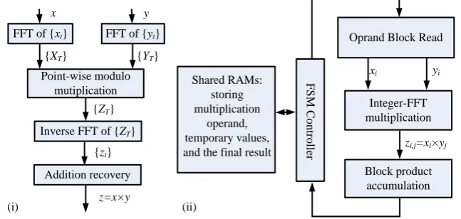
Fig. 1. (i) Diagram of the Integer-FFT multiplication algorithm; (ii) Overview of the proposed super-size hardware multiplier architecture
In the following of this subsection, we take an example, , to explain the operation of the proposed architecture. It is assumed that the super-size operands, and , are already stored in the shared RAMs before the multiplication starts. The input parameters to the proposed multiplier are divided into two groups. The first group re-lates to multiplication operands, ( -bit) and ( -bit). The second group is the Integer-FFT related parameters as described in Section 2.2. The steps of computing are as follows:
Step-1: In this step the operands are read from the shared RAMs. The operand is processed as a sequence of -bit data blocks, with
, from
LSB to MSB. Similarly, the sequence with
is obtained. Each
iteration, -bit and -bit are read into the proposed Integer-FFT multipli-er. Therefore, the total count of RAM read access is
due to the use of
school-book multiplication method.
Step-2: The Integer-FFT multiplication is performed to calculate the block product, , as described in Algorithm 1.
Step-3: Following the school-book multiplication method, this step accumulates the block products to obtain the final product, . This step also determines how to write/read the partial products to/from the shared RAMs. The final product, , is written to the share RAM as -bit data blocks, with
,
from LSB to MSB as follows:
─ Step-3.1: Read the -bit partial product, , from the shared RAMs into the
─ Step-3.2: Write the partial/intermediate block product into the shared RAMs. In this step, the block product, , is processed as two -bit parts from LSB
to MSB, and . If , is directly
written into memory, and remains the same; else if and , is written to memory; else if and , the addition, , is performed prior to writing
memory; else if and , is
writ-ten to memory. When , is kept in an on-chip register
array for faster accumulation.
─ Step-3.3: Determine the index of the operand data block to be read and de-termine the conditions for iterating the block multiplication as follows: If , increment , then go to Step-1; Else if
and , reset , increment , then go to Step-1; Else when
and
, the whole multiplication is completed.
In the following sections, the key components in the proposed multiplier architecture are described. In all the following diagrams the outputs of multiplication and sub-modules are registered.
3.2 The FFT/IFFT Module and Its Butterfly Unit
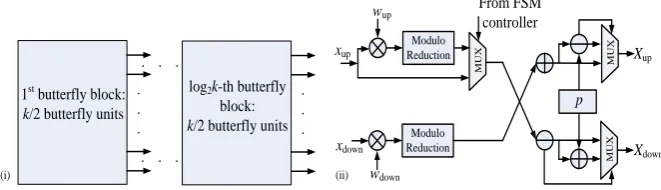
There are various different FFT algorithms and architectures that can be used to im-plement Equations (4) and (6) for different tradeoff purposes [18, 19]. In this paper, the radix-2 fully parallel architecture is adopted for the FFT and IFFT in order to ob-tain the highest multiplication throughput. The architecture is illustrated in Fig. 2(i). For example, there are butterfly stages for a -point FFT, and each butterfly stage is composed of parallel butterfly units, which is plotted in Fig. 2(ii).
(ii)
1st butterfly block:
k/2 butterfly units . . .
log2k-th butterfly block:
k/2 butterfly units . . . . . .
. . .
(i) wdown
Xup
Xdown
xup
xdown
Modulo Reduction
M
U
X
M
U
X
M
U
X
wup
Modulo Reduction
From FSM controller
p
Fig. 2. (i) The radix-2 parallel FFT diagram; (ii) The proposed FFT/IFFT butterfly unit
twiddle factors, then is used in the final IFFT butterfly stage, while the other stages still use . In order to meet the butterfly requirement of both of FFT and IFFT, a unified butterfly unit is proposed in Fig. 2(ii). The multiplication operation at the bottom left-hand side in Fig. 2(ii), , is the same for all FFT/IFFT butterfly stages, as well as the operation / as shown on the right-hand side
of Fig. 2(ii). However, the operation of illustrated on the upper left-hand
side of Fig. 2(ii) is only required at the final stage of the IFFT.
In our designs, if the special modulus form as listed in Table 3 is used, each ( -bit -bit) multiplier in a butterfly is implemented as bit-shifting, as the -th primitive root of unit is equal to 2 in this situation. Otherwise, each butter-fly multiplier is designed using a multi-stage pipelined multiplier, which is imple-mented using the FPGA embedded multipliers through the use of the Xilinx Core Generator [21] tools. This prevents the multipliers becoming the timing performance bottleneck in our design.
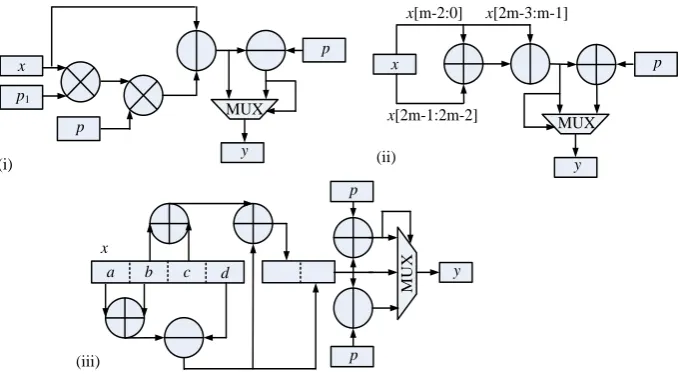
3.3 The Modular Reduction Module
The addition/subtraction modular reduction is very simple and is illustrated in the right-hand part in Fig. 2(ii). Therefore, this subsection introduces the modular reduc-tion unit used after the butterfly and point-wise multiplicareduc-tion. Three reducreduc-tion meth-ods are designed and tested in our work: the first is the Barrett modular reduction that can be used for any modulus ( here), the second is the simplest reduc-tion method of the three that is only suitable for a modulus with the special form , and the third is suitable for the Solinas modulus [24].
x
y
a b c d
p
p
M
U
X
p x
MUX
y x[m-2:0] x[2m-3:m-1]
x[2m-1:2m-2]
y
MUX
p1
p
p x
(i) (ii)
(iii)
The Barrett reduction architecture is shown in Fig. 3(i). Following the Barrett re-duction algorithm outline in Section 2, in our design we set and , thus, , and the pre-computed constant number in Fig. 3(i) is bits.
The design of the special form modulus reduction algorithm [14] is shown in Fig. 3(ii). The input parameters are ( -bit) and , the reduction is easily to be obtained using the logic in Fig. 3(ii) as follows: let and ; If
, ; else . As no multiplication is required here, this circuit obvi-ously consumes less hardware resource than Barrett reduction, and its speed perfor-mance is better.
The design of the Solinas modulus reduction is shown in Fig. 3(iii). If the Solinas modulus is used, the 128-bit multiplication product can be ex-pressed as , where , , and are 32-bit numbers. As
and , the reduction can be quickly
com-puted as . Thus, the upper-half 64-bit ( ) and the lower-half 64-bit ( ) results can be computed inde-pendently. As the result of is within the range of ( , ), an addition, a subtraction and a 3:3 multiplexer are needed for the final reduction. Alt-hough it is a little more complex than the special modulus form, it is much simpler than the Barrett reduction as no multiplication is required. However, according to the condi-tion described in Seccondi-tion 2.2, not every Solinas modulus is suitable for the Integer-FFT algorithm [14, 19].
3.4 The Addition Recovery and Product Accumulation Module
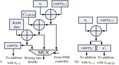
The addition recovery module is responsible for converting the IFFT outputs back to an integer by resolving a very long carry chain, as is shown in Equation (7). The product accumulation module is used to generate intermediate product results that can be written to memory. As these two modules are tightly coupled together in our pro-posed design, they are described in the same section.
The addition recovery architecture is composed of two parts, respectively depicted in Fig. 4(i) and 4(ii). The part in Fig. 4(i) is a parallel two-by-two adder tree, which means at each addition level, the adjacent two entries are added from the least signifi-cant entry to the most signifisignifi-cant entry. Let represent the data bus bit-width between our super-size multiplier and the shared RAMs. There are in total levels two-by-two adder trees (provided suitable values of and are chosen). Let the sequence with be the result after levels two-by-two addition. The addition results in each level are registered. Otherwise, a very long carry chain will become the time performance bottleneck of the design. It can be shown that the first useful -bit output value is included in , the second available -bit product can be obtained by
, and the third -bit product can be obtained by . Therefore, this can be achieved by a registered carry chain addition, which is illustrated in Fig. 4(ii).
chain of length is needed to generate the -bit result, the parameter should be carefully chosen to avoid this carry chain becoming the performance bottleneck. This parameter is determined by iterative experiments in our implementation (here the values are used for the four test groups in Table 4 respectively).
zk-1 zk-2
. . .
<<b
zk-3 zk-4
<<b
<<2b
<<d <<2b
z3 z2
<<b
z1 z0
<<b
<<2b
<<d
z'0
z'kb/d-1
. . . . . . . . . . . . . . . z'2 To product accumulation >>d z'1 z'0 To product accumulation >>d z'kb/d-1 To product accumulation >>d . . . (i) (ii)
Fig. 4. The proposed addition recovery architecture: (i) a parallel two-by-two adder tree used as the 1st part; (ii) a serial and registered carry chain used as the 2nd part.
si carryi-1
s'i+kb/2d
carryi RAM data MUX From FSM controller Writing into RAMs To addition
with si+1
(i) (ii)
si carryi-1
carryi s'i
To addition with si+1
To addition with si-kb/2d
Fig. 5. The proposed serial and registered multiplication product accumulation architecture: (i) when ; (ii) when
From the carry chain logic perspective, the logic in Fig. 4(ii) should be executed after that in Fig. 4(i). Actually in our design, they are concurrently and pipelined exe-cuted. We take the example in Step-3.2 to explain in Section 3. Each block product,
, is processed as two -bit parts, and . In the first
block round (i.e. ), is first generated and written into memory. At the same time, cannot be obtained due to the lacking of carry bits. Then from the next block iteration (i.e. ), and
can be calculated simultaneously, as all the parameters in Fig. 4(i) and
Fig. 4(ii) are already ready to use from this moment.
4
The Proposed FHE Encryption and Super-Size Modular
Reduction Architecture
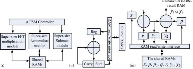
The proposed hardware architecture for the two encryption primitives in CMNT and CNT are plotted in Fig. 6(i). These two primitives share the same architecture but with different FSM controller logic (i.e., different accumulation and multiplication schedule procedure). Due to that only one instance of the proposed multiplier is im-plemented in our architecture, the FHE encryption architecture is tightly coupled with the super-size Barrett modular reduction using the FSM controller. Thus, the over-view diagram in Fig. 6(i) can also represent the proposed architecture of the super-size Barrett reduction, which means that all the multiplications, in Equations (1) and (2) and the super-size Barrett reduction, are completed by the single Integer-FFT in-stance.
A FSM Controller
Super-size Accumulate module Super-size Subtract module Super-size FFT multiplication module Shared RAMs
(i) (ii) Carry Sum
Reg R A M r e a d /w ri te in te rf a c e S h a re d R A M s (iii)
Indicate the correct result RAM:
y1 or y2
The shared RAMs:
x, p, p1, q, r, y1, y2 RAM read/write interface
y1 y2
p
r x
Fig. 6. The proposed FHE encryption and super-size Barrett modular reduction architecture: (i) an overview diagram; (ii) a super-size accumulation module for FHE encryption; (iii) the sub-traction module for the super-size Barrett reduction.
should be defined as according to the adopted Barrett reduction algorithm [25]. As the bit-length of or is much less than and the bit-length of the accumula-tion counter is much less than , it is clear that is also much less than . This is beneficial to the super-size Barrett reduction hardware design, as it allows more flexi-bility to choose the parameters. In this super-size situation, Equation (8) becomes (9):
(9)
Here, we still use the symbols and in our explanation. As , and are super-size parameters, it is impossible to directly load all the required bits of and into the multiplier directly. Therefore, we need to iteratively access the memory to obtain the full values. An implementation issue of the super-size Barrett reduction is how to choose the suitable value of and in Equation (9) so that the correct val-ues of and can be read out from the right address of the shared RAMs when computing and . In our work, this issue is solved by relating the value of and to the data bus bit width, , as given in Equations (10) and (11),
(10)
(11) In Equation (10) it is assumed that in super-size FHE implementation. Through setting the initial RAM storage address of and in the shared RAMs to 0, the above parameter setting makes sure the initial read address of , , is a multiple of , and the starting read address of , , is also a multiple of . At the same time, Equation (10) obviously meets the requirement of , and Equation (11) also has as it is mentioned that both and are much smaller than . Thus, the procedure of the proposed super-size modular reduction is as follows:
Step-1: The constant number is pre-computed and stored in the shared RAM before the reduction starts.
Step-2: Read from its RAM address , and read from its RAM address 0, then use the super-size FFT multiplication module to calculate .
Step-4: Read , and from their RAM address 0, and use the super-size sub-tract module to calculate , and output a signal that indicates which of or is the correct reduction result.
As the subtraction also a super-size operation, a super-size subtraction module is designed in Fig. 6(iii) to complete the required subtraction operation in the super-size Barrett reduction. It is essentially a successively applied -bit subtraction operation, but a memory read/write interface is added to extend its bit width
5
Implementation, Performance and Comparison
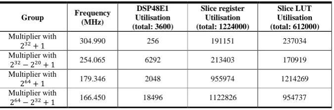
All the proposed architectures were designed and implemented using Xilinx FPGA technology. Modelsim 6.5a was used as the functional and post-synthesis timing sim-ulation tool. The synthesis tool used was Xilinx ISE Design Suite 14.4. The synthesis strategy is set to balance between speed and area. The optimisation objective is set to speed. The target device is Virtex-7 XC7VX980T. The test vectors are generated as random numbers using C++ according to the parameter requirements in Table 1 and Table 2.
The proposed super-size multiplier architecture has been implemented as a fully pipelined and parallel circuit. At the outer interface, three RAM read buses and one RAM write bus are implemented, so that the two super-size multiplication operands can be simultaneously read into the multiplier, and at the same time the final block product accumulation can also be executed simultaneously. At the inner layer, the Integer-FFT is also pipelined.
From the Table 3, it can be found that the base unit bit-length is chosen as the max-imum even number of the suitable numbers according to the parameter requirements described in Section 2. The reason is that the basic computation bit-length in Integer-FFT is determined by the modulus bit-length rather than the base unit bit-length, so increasing the base unit bit-length will not decrease the speed performance of Integer-FFT’s multiplication and addition. However, the base unit bit-length is related to the multiplication product throughput, that is, the larger the base unit bit-length, the less the consumed clock cycle count.
In our implementation, the ratio of multiplication operand’s block bit-length and the data bus bit-width (for both RAM read and write),
, to be equal to 8. Thus, the
data bus bit-width is respectively equal to 32, 48, 192 and 224 corresponding to the four group parameters in Table 3. It means that the clock count is equal to 8 for each -bit input operand, and the clock cycle count is also equal to 8 for each output block product except the first block product, according to our described hardware architecture. Meanwhile, the pipeline stage count in each FFT butterfly stage is de-signed to be also equal to 8, which accounts for all the -bit multiplication, addi-tion/subtraction and modular reduction.
prod-uct, and the second part is determined by the count of block products multiplying a fixed parameter for a pipelined architecture. It is equal to 8 in our design.
Let , and respectively be the count of pipeline stage in a FFT/IFFT but-terfly, in a point-wise multiplication, and in the addition recovery. Then, the time latency of the preparation work is equal to , where denotes the latency for reading the operand, and
denotes the block product computation latency. Next, the common time
latency of outputting each block products is analysed according to the logic described in Step-3.2 and Step-3.3 in Section 3. If , -bit intermediate product is written into memory, and the latency is equal to ; if , -bit intermediate product is written into memory, and the latency is . As there are totally block products, in which there are blocks with the condition . As in our design we have , therefore, combining the two parts, the whole time
laten-cy can be expressed as:
(12)
We have implemented four different designs using the four groups of parameters in Table 3. For each design, the FFT point num is fixed, unrelated to the multiplication operand bit-length. With the input multiplication operand bit-length increasing, quickly becomes much smaller than , as the data bus bit-width is fixed. Therefore, the time latency of the proposed implementations with the four forms of modulus is almost the same, which can be estimated by multiplying the total count of block products, , and the output latency of each block product, .
For the small size 33-bit 33-bit, 32-bit 32-bit, 65-bit 65-bit and 64-bit 64-bit multiplication used in FFT butterfly and point-wise multiplication, Xilinx Core Gen-erator is employed to generate a 4 stage pipelined multiplier using the embedded mul-tipliers on the Virtex-7 FPGA device. Meanwhile, in order to meet the demand of the addition recovery latency, that is , the adder tree length is equal to , 4,
4, 8, and 8 in our implementations respectively.
Table 4. The synthesis results of the proposed super-size multiplier.
Group Frequency (MHz)
DSP48E1 Utilisation (total: 3600)
Slice register Utilisation (total: 1224000)
Slice LUT Utilisation (total: 612000) Multiplier with
304.990 256 191151 237034
Multiplier with
254.065 6292 213403 170919
Multiplier with
179.346 2048 955974 1214269
Multiplier with
The synthesis results of the proposed super-size multiplier are displayed in Table 4. The hardware resource utilisation and frequency of the two designs with the special modulus ( and ) are obviously better than the multipliers with the gen-eral modulus ( ) and the Solinas modulus ( ). The reason the special modulus multiplier requires the smallest hardware resource is that it does not need multiplication in the FFT butterfly unit and no multiplication is needed for reduction with the special modulus. The reason the Solinas modulus multiplier re-quires more hardware than the general modulus multiplier is that it does not need multiplication in the modular reduction units. It can also be seen that the smallest bit-length modulus multiplier has the highest frequency, as the four multipliers needed for the point-wise multiplication in the Integer-FFT algorithm contain the critical path, and are implemented as 4 stage pipelined multipliers. However, this does not mean that the super-size multiplier with the special modulus will definitely outper-form the other two, as the other two multipliers allow a larger base bit-length that implies that in one clock cycle the Solinas modulus multiplier can produce the longest product.
Meanwhile, we can find that only the multiplier with the smallest modulus
is within the hardware resource budget, and there are not enough hardware
resources for the other architectures. Thus, the conclusion is that the parallel FFT architecture is not suitable for a practical or implementable design due to the exces-sive hardware cost, although this FFT architecture has the highest product throughput.
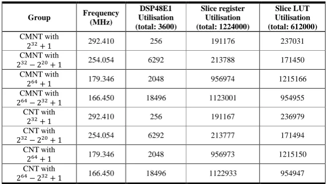
Table 5. The synthesis results of the FHE encryption primitives.
Group Frequency (MHz)
DSP48E1 Utilisation (total: 3600)
Slice register Utilisation (total: 1224000)
Slice LUT Utilisation (total: 612000) CMNT with
292.410 256 191176 237031
CMNT with
254.054 6292 213788 171450
CMNT with
179.346 2048 956974 1215166
CMNT with
166.450 18496 1123001 954955
CNT with
292.410 256 191167 236979
CNT with
254.054 6292 213777 171494
CNT with
179.346 2048 956973 1215150
CNT with
166.450 18496 1122933 954947
Barrett reduction can be estimated at twice the time cost that is required by a super-size multiplication with the input operand’s bit-length.
The two encryption primitives in Equation (1) and (2) have been implemented by adding a super-size accumulation module following the super-size Barrett reduction. It can be seen as a serial procedure of two stages. In the first stage, the super-size accumulation module and the super-size multiplier are parallel executed; in the se-cond stage, the super-size Barrett reduction is executed. The reason is that there is only one super-size multiplier is implemented. The synthesis results of the implemen-tations of FHE encryption primitives are listed in Table 5. It can be seen that the fre-quency and hardware resource utilization are almost the same as that in Table 4. The synthesis performance of CMNT and CNT is also nearly identical. The reason is that the controller part only occupies a very small percentage of hardware resource com-pared to the super-size multiplier, and the only difference between the CMNT’s and CNT’s controller parts is the different multiplier scheduling procedures.
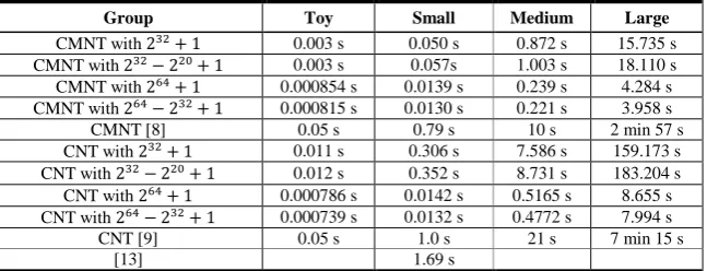
Table 6. The average running time of the proposed FHE encryption designs.
Group Toy Small Medium Large
CMNT with 0.003 s 0.050 s 0.872 s 15.735 s
CMNT with 0.003 s 0.057s 1.003 s 18.110 s CMNT with 0.000854 s 0.0139 s 0.239 s 4.284 s CMNT with 0.000815 s 0.0130 s 0.221 s 3.958 s
CMNT [8] 0.05 s 0.79 s 10 s 2 min 57 s
CNT with 0.011 s 0.306 s 7.586 s 159.173 s
CNT with 0.012 s 0.352 s 8.731 s 183.204 s CNT with 0.000786 s 0.0142 s 0.5165 s 8.655 s CNT with 0.000739 s 0.0132 s 0.4772 s 7.994 s
CNT [9] 0.05 s 1.0 s 21 s 7 min 15 s
[13] 1.69 s
The running time of the proposed hardware implementations of FHE encryption primitives using the 4 group parameters listed in Table 1 and Table 2 is provided in Table 6, and the previously reported corresponding software results are also given here. The running time is obtained by averaging the simulated latency of the test vec-tors and multiplying by the synthesis frequency. It can be seen that although the spe-cial modulus multiplier has a higher frequency, it needs more running time than the Solinas modulus multiplier. The reason is that for the proposed multiplier, the multi-plication product throughput is mainly determined by the product of the data bus bit-width, the base unit bit-length and the frequency, rather than only the frequency, which can be deduced from the time latency expression in Equation (12). Comparing the four group parameters in Table 3, it is also easy to see that although the special modulus can use twiddle factor of 2, its obvious disadvantage is that its base unit length is much smaller than the other two kinds of modulus when almost the same bit-length modulus is employed. Therefore, for the proposed FHE encryption architec-ture, the Solinas modulus is the best choice in our proposed designs, which enables a comparable simpler modular reduction and a larger base unit bit-length.
im-plementations are 61.34 and 67.65 times faster than the software imim-plementations of CMNT and CNT respectively for the toy parameter group. And the proposed designs also respectively achieve a time improvement of 44.72 and 54.42 for the large group. It must be noted that only the experimental results using small FFT parameters (i.e., and ) are reported in this paper. As the product of the data bus bit-width and the frequency determines the proposed super-size multiplier product throughput performance, we have enough reason to believe that there is still a great potential to improve the time performance for encryption primitives in FHE over the integers if larger FFT parameters are used. For example, the recent batch FHE over the integers proposed in [26] shows that the parallel super-size multiplication can be applied to improve the FHE encryption speed.
6
Conclusion
In this paper, the first complete hardware implementations of two encryption primi-tives employed in schemes of FHE over the integers proposed by Coron et al. are presented. For this purpose, an Integer-FFT based super-size hardware multiplier module and a super-size Barrett modular reduction module are proposed. These pro-posed hardware architectures are designed and verified on a Xilinx Virtex-7 device using four groups of Integer-FFT parameters. When the super-size multiplier is im-plemented with a Solinas Integer-FFT modulus, the synthesis results show that our hardware implementations achieve speed improvement factors of 44.72 and 54.42 compared to the corresponding software implementations for the large scale test data used in FHE over the integers. Meanwhile, as our implementations only use 128 point FFT and small base unit bit-length, 24 and 28, for the super-size hardware multiplier, there is still great potential to further improve the encryption speed in FHE over the integers. Recently research improvements in this area such as the batch FHE over the integers [26] confirm that this potential indeed exists for both hardware architecture and implementation developments.
References
1. Gentry, C.: A fully homomorphic encryption scheme. Ph.D. thesis, Stanford University, (2009). Http://crypto.stanford.edu/craig.
2. Gentry, C.: Fully homomorphic encryption using ideal lattices. The 41st annual ACM sym-posium on Theory of computing. pp. 169–178. ACM (2009).
3. van Dijk, M., Gentry, C., Halevi, S., Vaikuntanathan, V.: Fully homomorphic encryption over the integers. EUROCRYPT 2010, LNCS, vol. 6110, pp. 24–43. Springer (2010). 4. Smart, N.P., Vercauteren, F: Fully homomorphic encryption with relatively small key and
ciphertext sizes. PKC 2010, LNCS, vol. 6056, pp. 420–443. Springer (2010).
5. Brakerski, Z., Vaikuntanathan, V.: Efficient Fully Homomorphic Encryption from (Stand-ard) LWE. FOCS (2011).
7. Brakerski, Z., Gentry, C., Vaikuntanathan, V.: Fully Homomorphic Encryption without Bootstrapping. Cryptology ePrint Archive, Report 2011/277 (2011).
8. Coron, J.S., Mandal, A., Naccache, D., Tibouchi, M: Fully Homomorphic Encryption over the Integers with Shorter Public Keys. CRYPTO 2011, LNCS, vol. 6841, pp. 487–504. Springer (2011).
9. Coron, J.S., Naccache, D., Tibouchi, M: Public key compression and modulus switching for fully homomorphic encryption over the integers. EUROCRYPT'12. pp. 446–464. Springer (2012).
10. Gentry, C., Halevi, S.: Implementing Gentry's fully homomorphic encryption scheme. EUROCRYPT 2011, LNCS, vol. 6632, pp. 129–148. Springer (2011).
11. Gentry, C., Halevi, S., Smart, N.P.: Homomorphic Evaluation of the AES circuit. Cryptol-ogy ePrint Archive, Report 2012/099 (2012).
12. Lauter, K., Naehrig, M., Vaikuntanathan, V.: Can Homomorphic Encryption be Practical? Cryptology ePrint Archive, Report 2011/405 (2011).
13. Wang, W., Hu, Y., Chen, L., Huang, X., Sunar, B.: Accelerating fully homomorphic en-cryption using GPU. High Performance Extreme Computing (HPEC), pp. 1-5. IEEE (2012).
14. Schönhage, A., Strassen, V.: Schnelle multiplikation grosser zahlen. Computing, vol. 7, no. 3, pp. 281–292. (1971).
15. Barrett, P.: Implementing the rivest shamir and adleman public key encryption algorithm on a standard digital signal processor. In Advances in CRYPTO’86. pp. 311–323. Spring-er, (1987).
16. Cousins, D.B., Rohloff, K., Peikert, C., Schantz, R.: SIPHER: Scalable implementation of primitives for homomorphic encryption–FPGA implementation using Simulink. High Per-formance Extreme Computing Conference (2011).
17. Cousins, D.B., Rohloff, K., Peikert, C., Schantz, R.: SIPHER: An update on SIPHER (Scalable Implementation of Primitives for Homomorphic EncRyption) — FPGA imple-mentation using Simulink. High Performance Extreme Computing Conference (2012). 18. Craven, S., Patterson, C., Athanas, P.: Super-sized multiplies: how do FPGAs fare in
ex-tended digit multipliers. 7th International Conference on Military and Aerospace Program-mable Logic Devices. (2004).
19. Emmart, N., Weems, C.: High precision integer multiplication with a gpu using strassen’s algorithm with multiple fft sizes. Parallel Processing Letters, vol. 21, no. 3, p. 359. (2011). 20. http://gmplib.org/manual/Multiplication-Algorithms.html#Multiplication-Algorithms. 21. Xilinx Product Specification: LogiCORE IP Multiplier v11.2.
http://www.xilinx.com/support/documentation/ip_documentation/mult_gen_ds255.pdf 22. Montgomery, P.: Modular multiplication without trial division. Mathematics of
computa-tion, vol. 44, no. 170, pp. 519–521. (1985).
23. Kalach, K., David, J.P.: Hardware implementation of large number multiplication by FFT with modular arithmetic, the 3rd International IEEE-NEWCAS Conference, pp.267 – 270. (2005).
24. Solinas, J. A.: Generalized Mersenne Numbers, Issue 39 of Research report (University of Waterloo. Faculty of Mathematics). (1999).
25. Dhem, J. F.: Design of an efficient public-key cryptographic library for risc-based smart cards. PhD thesis. (1998).