ABSTRACT
HOU, DANQIONG. A Physics-Based AlGaN/GaN HFET Compact Model for Implementation in Circuit Simulators. (Under the direction of Dr. Robert J. Trew and Dr. Griff L. Bilbro.)
AlGaN/GaN heterojunction field-effect transistors (HFETs) are promising RF
tran-sistors for use in high-power and high-frequency circuit applications. These HFETs
possess a combination of high current density capability and high breakdown voltage due
to the desirable physical properties of the materials, such as high critical electric field for
breakdown, high electron mobility and saturated carrier velocity, high carrier density in
the channel, lower dielectric constant compared to the conventional materials, and
im-proved thermal conductivity when epitaxially grown on semi-insulating SiC substrates.
These parameters permit the HFET to operate at high RF voltage and current, which
results in high power operation at high frequency [1], [2].
The technology for fabricating devices and circuits in AlGaN/GaN is developing
rapidly, and this rapid development is creating a need for improved device models. To
date no commercially available HFET model for use in harmonic-balance circuit
simula-tors exists that can predict the large-signal RF operation of an HFET or a MMIC before
the active device is fabricated, characterized, and fitted.
In this work, a new physics-based compact model for AlGaN/GaN HFETs has been
re-ported. The new model is programmed in Verilog-A, an industry-standard compact
mod-eling language, and implemented in the circuit simulator Microwave Office (MWOTM).
The new model is developed, based upon separating the conducting channel of the
HFET into a series of zones, based upon operational physics [3]. According to the
the conduction current formulation can be derived in terms of the electrical nodes in
the devices. Then the charge storages and corresponding displacement current can be
obtained.
The HFET model is generalized to suit different fabrication process by introducing a
curvature parameter in the v-E relationship [4] for electrons in the conducting channel
of the HFET in order to control the sharpness of the knee of the I-V characteristics. The
charge deficit zone has been considered in the drain access for triode operation as well as
saturation operation to ensure continuity of the terminal characteristics. The pinch off
voltage is modified to take into account different Al mole fractions in the AlGaN barrier
layer in the AlGaN/GaN HFET. Finally, it is necessary to consider channel breakdown in
order to accurately simulate RF performance (RF output power, Power Added Efficiency
(PAE) and gain) at high RF power operation.
The model is written in Verilog-A language and implemented it in MWOTM. The
model has been calibrated and verified by comparison of its predictions for dc and RF
performance against measured data and SilvacoTM simulation results for an experimental S-Band AlGaN/GaN HFET amplifier. Good agreement is obtained.
The new model permits the dc, small-signal, and large-signal RF performance for
the transistor to be determined as a function of the device geometric structure and
design features, material composition parameters, and dc and RF operating conditions.
The new physics-based HFET model does not require extensive parameter extraction to
determine model element values, as commonly employed for traditional equivalent-circuit
based transistor models. Therefore, it′s suitable for use in commercial harmonic-balance
microwave circuit simulators, and permits the co-design and optimization of HFETs in
c
Copyright 2012 by Danqiong Hou
A Physics-Based AlGaN/GaN HFET Compact Model for Implementation in Circuit Simulators
by Danqiong Hou
A dissertation submitted to the Graduate Faculty of North Carolina State University
in partial fulfillment of the requirements for the degree of
Doctor of Philosophy
Electrical Engineering
Raleigh, North Carolina
2012
APPROVED BY:
Dr. Leda M. Lunardi Dr. Zhilin Li
Dr. Robert J. Trew Dr. Griff L. Bilbro
DEDICATION
BIOGRAPHY
Danqiong Hou was born in datong, China. She joined Beijing University in 1999. Four
years later she graduated with a Bachelor of Science degree in device physics. Upon
completion of the Bachelors program she continued on as a Master student at Beijing
University in August 2003 and got her Master of Science degree in Microelectronics in
May 2006. In August 2006, she attended the Department of Electrical and Computer
Engineering at North Carolina State University as a Ph.D. student under the supervision
of Dr. Robert J. Trew and Dr. Griff L. Bilbro. Her Ph.D. research focused on developing
a physics-based AlGaN/GaN HFET compact model suitable for use in microwave circuit
simulators. Danqiong’s research interests lie in modeling/simulation and design of
ACKNOWLEDGEMENTS
I would like to thank my advisors Dr. Robert J. Trew and Dr. Griff L. Bilbro for
their guidance and support. They have been providing inspiration and encouragement
throughout this work. I have learned a lot about methodology of research and life from
them. I feel really lucky to have these two great professors as my advisors. I am also
grateful to Dr. Leda M. Lunardi and Dr. Zhilin Li for serving on my Ph.D. advisory
committee.
I thank Dr. Ki Wook Kim, who was extremely helpful in my first year as a Ph.D
student and inside his classes.
I thank my graduate student colleagues Ryan Schimizzi, Arunesh Goswami, and fellow
colleagues who have already graduated Hong Yin, Yueying Liu, Weiwei Kuang for the
beneficial discussion and the good working environment they provided. Their wisdom
and creativity have been invaluable to me.
I also want to thank my friends at NC State and elsewhere, who have made my life
here as a Ph.D. student both enjoyable and bearable during certain times.
Finally, but most importantly, I am grateful to my parents for their unconditional
support. I owe a lot to my beloved husband Jie Hu for his patience and support. I thank
TABLE OF CONTENTS
LIST OF TABLES . . . vii
LIST OF FIGURES . . . viii
Chapter 1 Introduction . . . 1
1.1 Overview . . . 1
1.2 Motivation & Research Objectives . . . 3
1.3 Original Contributions . . . 4
1.4 Dissertation Outline . . . 5
Chapter 2 Background and Prior research in HFET models . . . 6
2.1 Overview of FET Models . . . 6
2.1.1 Empirical Model . . . 6
2.1.2 2-D Physics Model . . . 7
2.1.3 Compact Physics-Based Model . . . 8
2.2 Conduction Current Formulation . . . 9
2.3 Displacement Current Formulation . . . 11
2.3.1 Division by Charge . . . 14
2.3.2 Division by Capacitance . . . 15
2.3.3 Division by Current . . . 16
2.4 Summary . . . 19
Chapter 3 Model Theory Description . . . 20
3.1 Introduction . . . 20
3.2 Model Discription . . . 22
3.2.1 Zone Model of the AlGaN/GaN HFET . . . 22
3.2.2 Generalized Velocity-Field Relationship for Carrier Electrons . . . 27
3.2.3 Pinch Off Voltage . . . 30
3.3 Physics of the zones . . . 32
3.3.1 Zones Z1 and Z5, Source Neutral Zone (SNZ) . . . 32
3.3.2 Zone Z2, Intrinsic FET Zone (IFZ) . . . 35
3.3.3 Zone Z3, Space-Charge Limited Zone (SLZ) . . . 38
3.3.4 Zone Z4, Charge Deficit Zone (CDZ) . . . 39
3.3.5 Zone Z5, Drain Neutral Zone (DNZ) . . . 40
3.4 Displacement Current . . . 42
3.5 Breakdown . . . 44
3.6 Summary . . . 46
4.1 Introduction . . . 48
4.2 Numerical Method for Solving the Model . . . 51
4.3 Analytical Method for Solving the Model . . . 54
4.3.1 Conduction Current . . . 55
4.3.2 Displacement Current . . . 66
4.4 Summary . . . 77
Chapter 5 Model Implementation in Circuit Simulator and Model Ver-ification . . . 78
5.1 Introduction . . . 78
5.2 Verilog-A Compact Model . . . 79
5.3 Model Implementation in MWOTM . . . . 80
5.4 Model Verification, Results and Discussion . . . 82
5.4.1 DC Simulation . . . 82
5.4.2 Small Signal Simulation . . . 86
5.4.3 Broad-Band S-Parameters . . . 94
5.4.4 Large Signal Simulation . . . 96
5.5 Summary . . . 102
Chapter 6 Conclusion and Future Work . . . 106
LIST OF TABLES
Table 1.1 Comparison of Semiconductor Properties. . . 2
Table 3.1 Energy band parameters. . . 31
Table 4.1 List of symbols used in formula derivation. . . 52
LIST OF FIGURES
Figure 1.1 Basic HFET structure. . . 3
Figure 2.1 Gate-channel charge is partitioned into source charge and gate-drain charge. . . 14 Figure 2.2 Gate-channel capacitance is partitioned into gate-source capacitance
and gate-drain capacitance. . . 16 Figure 2.3 Gate current is partitioned into gate-source current and gate-drain
current. Qg is a voltage dependent charge source. . . 17
Figure 2.4 Simplified equivalent circuit of Fig. 2.3. Qg is a voltage dependent
charge source. . . 18 Figure 2.5 Simplified equivalent circuit of Fig. 2.5. Qg is a voltage dependent
charge source. . . 18
Figure 3.1 Schematic cross-section of a basic AlGaN/GaN HFET structure, show-ing the physical parameters of the NCSU HFET model. Four param-eters describe layout: W,Ls, L−g,Ld. Four parameters describe the
barrier layer: χAlGaN, Alx, tAlGaN,nox. Seven parameters describe the
GaN buffer: εGaN, EgGaN, tGaN for the GaN itself. Three parameters
for electron transport in the GaN: µ0, vsat, β. Two parameters for its
interface with AlGaN: nss, npiezo. The gate metal is characterized by
its electron affinity χM. . . 22
Figure 3.2 Cross-section of HFET model in (a) triode operation which has four physical zones, and (b) saturated operation which has 5 physical zones. The voltages at the boundaries between zones are labeled. Except for Z3, the dotted line indicates the electron path in the 2DEG just below the AlGaN/GaN interface. In Z3, the 2DEG is disrupted and the electrons disperse away from the interface to form a net space charge in the GaN. . . 24 Figure 3.3 Plotting v-E relationship in (a) for various β values, and in (b)
com-paring (3.1) (red) with that of the two-field model (blue). . . 29 Figure 3.4 Rs as a function of the conductance current with different beta. The
values of β are 2, 1.5 and 1.2 respectively. The length of the source access region is 1.2um. . . 35 Figure 3.5 Current-voltage characteristics for a 0.8um HFET with breakdown (red
Figure 4.1 Modeling the channel of (a) 3-terminal FET as (b) serially connected 5 zones. . . 49 Figure 4.2 The lower and upper limits of the integral (4.14), Vsi and Vc, as
func-tions of Ids. . . 53
Figure 4.3 f(Ids) monotonically increases withIds. . . 54
Figure 4.4 Flowchart to calculate the current as a function ofVgs and Vds. . . 55
Figure 4.5 Modeling the channel of the 3-terminal FET as serially connected 3 blocks. . . 56 Figure 4.6 The conduction current as a function of the voltage drop across the
source access region. . . 58 Figure 4.7 The transition voltage as a function of Vgt−Vsi, with different β. . . 62
Figure 4.8 The transition current as a function ofVgt−Vsi, with different β. . . 63
Figure 4.9 The conduction current as a function of the voltage drop across the drain access region. . . 64 Figure 4.10 Voltage-controlled charge sources in the HFET. . . 68 Figure 4.11 Capacitances related to the voltage-controlled charge sources. . . 77
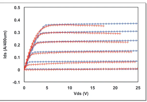
Figure 5.1 Current-voltage characteristics simulated by MWOTM for the HFET model (blue lines), along with experimental measurements (red lines) for a HFET with 0.8um gate length and 400um width. Each of the six curves corresponds to aVgs value from -4V to 1V. All curves sweep Vds
from 0V to 20V. . . 82 Figure 5.2 Current-voltage characteristics simulated by MWOTM for the HFET
model (blue lines), along with experimental measurements (red lines) for a HFET with 0.85um gate length and 400um width. Each of the curves corresponds to a Vgs value from -2.5V to 1.0V with a step of
0.25V. All curves sweep Vds from 0V to 20V. . . 83
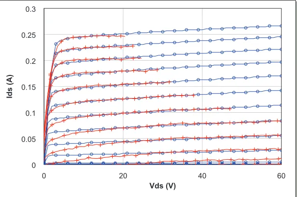
Figure 5.3 Current-voltage characteristics simulated by MWOTM for the HFET model (blue lines), along with experimental measurements (red lines) and results from SilvacoTM(green lines) for theW=400um,L
g=0.8um,
transistor under consideration. Each of the six curves corresponds to an integer Vgs value from -4V to 1V. All curves sweep Vds from 0V to
20V. . . 84 Figure 5.4 xc versusVds for theW=400um,Lg=0.8um, transistor under
consider-ation, withVgs=-1V. ”Red” is for SilvacoTMsimulation results, ”Blue”
is for the HFET model results from MWOTM. . . . 85 Figure 5.5 xc versusIds for the W=400um,Lg=0.8um, transistor under
consider-ation, withVgs=-1V. ”Red” is for SilvacoTMsimulation results, ”Blue”
Figure 5.6 Lengths of Z3 and Z4 as functions of drain bias for the W=400um,
Lg=0.8um, transistor under consideration, with Vgs = -1V and -3V.
All curves sweep Vds from 0V to 20V. . . 86
Figure 5.7 Transconductance as a function of gate bias for theW=400um,Lg=0.8um,
transistor under consideration, with Ld as a parameter. Vds = 1V and
3V. ”Red” is for Ld=2um, ”Blue” is for Ld=1um. All curves sweep
Vgs from -4V to 1V. . . 87
Figure 5.8 Transconductance as a function of gate bias for theW=400um,Lg=0.8um,
transistor under consideration, with Ls as a parameter. Vds = 1V and
3V. ”Red” is forLs=1.2um, ”Blue” is forLs=0.2um. All curves sweep
Vgs from -4V to 1V. . . 88
Figure 5.9 Transconductance as a function of drain bias for theW=400um,Lg=0.8um,
transistor under consideration, with Ld and Ls as parameters. Vgs =
-1V and -3V. ”Red” is forLd=2um,Ls=1.2um, ”Blue” is forLd=1um,
Ls=0.5um. All curves sweep Vds from 0V to 20V. . . 89
Figure 5.10 Output conductance as a function of drain bias for the W=400um,
Lg=0.8um, transistor under consideration, with Ld and Ls as
param-eters. Vgs = -1V and -3V. ”Red” is for Ld=2um,Ls=1.2um, ”Blue” is
for Ld=1um, Ls=0.5um. All curves sweep Vds from 0V to 20V. . . 90
Figure 5.11 Gate-source and gate-drain charges as functions of drain bias for the
W=400um, Lg=0.8um, transistor under consideration, with Vgs = -1
and -3V. All curves sweep Vds from 0V to 20V. . . 90
Figure 5.12 Gate-source and gate-drain charges as functions of gate bias for the
W=400um, Lg=0.8um, transistor under consideration, with Vds = 1
and 10V. All curves sweep Vgs from -4V to 1V. . . 91
Figure 5.13 Gate-drain extrinsic charge as a function of drain bias for theW=400um,
Lg=0.8um, transistor under consideration, with Vgs = -1 and -3V. All
curves sweep Vds from 0V to 20V. . . 92
Figure 5.14 Gate-drain extrinsic charge as a function of gate bias for theW=400um,
Lg=0.8um, transistor under consideration, with Vds = 1 and 10V. All
curves sweep Vgs from -4V to 1V. . . 93
Figure 5.15 Gate-source and gate-drain charges as functions of drain bias for the
W=400um, Lg=0.8um, transistor under consideration, with β as a
parameter. Gate bias is fixed at Vgs = -1V. All curves sweepVds from
0V to 20V. . . 93 Figure 5.16 Gate-source and gate-drain charges as functions of drain bias for the
W=400um, Lg=0.8um, transistor under consideration, with Ls as a
parameter. Gate bias is fixed at Vgs = -1V. All curves sweepVds from
Figure 5.17 Cgs and Cgd as functions of drain bias for theW=400um, Lg=0.8um,
transistor under consideration, with gate bias of Vgs = -1V and -3V.
All curves sweep Vds from 0V to 20V. . . 95
Figure 5.18 Cegs and Cegd as functions of drain bias for theW=400um, Lg=0.8um,
transistor under consideration, with gate bias of Vgs = -1V and -3V.
All curves sweep Vds from 0V to 20V. . . 95
Figure 5.19 Cgdeas functions of drain bias for theW=400um,Lg=0.8um, transistor
under consideration, with gate bias of Vgs = -1V and -3V. All curves
sweep Vds from 0V to 20V. . . 96
Figure 5.20 Comparison the S-parameters S11 and S22 simulated from SilvacoTM and from the HFET model with MWOTM, for theW=400um,L
g=0.8um,
transistor under consideration. The frequency is in the range of 0.1-10 GHz. The HFET is biased at Vgs=-3.15V and Vds=10V. ”Red” is for
SilvacoTM simulation results, ”Blue” is for the HFET model results from MWOTM. . . . 97 Figure 5.21 Comparison the S-parameters S12 and S21 simulated from SilvacoTM
and from the HFET model with MWOTM, for theW=400um,L
g=0.8um,
transistor under consideration. The frequency is in the range of 0.1-10 GHz. The HFET is biased at Vgs=-3.15V and Vds=10V. ”Red” is for
SilvacoTM simulation results, ”Blue” is for the HFET model results from MWOTM. . . . 98 Figure 5.22 Large signal simulation results including output power, power gain and
PAE obtained from the HFET model comparison to the measurement data for the W=400um, Lg=0.8um, transistor under consideration,
with and without (insertion graph) channel break down model. (”Red” is measurement data, ”Blue” is simulation results.) . . . 99 Figure 5.23 Large signal simulation results including output power, power gain and
PAE obtained from the HFET model comparison to the measurement data for the W=400um, Lg=0.85um, transistor under consideration,
with and without (insertion graph) channel break down model. (”Red” is measurement data, ”Blue” is simulation results.) . . . 100 Figure 5.24 PAE as a function of input power, with breakdown voltage as a
pa-rameter. . . 100 Figure 5.25 PAE as a function of input power, with breakdown resistance as a
parameter. . . 101 Figure 5.26 PAE as a function of input power, with 1st load harmonics (real part)
as a parameter. . . 101 Figure 5.27 PAE as a function of input power, with 2nd load harmonics (real part)
Figure 5.28 IM3 for the W=400um, Lg=0.8um AlGaN/GaN HFET under
consid-eration. The operation frequency is 2.14GHz, ∆f=0.3GHz. . . 103 Figure 5.29 Power spectrum for the W=400um, Lg=0.8um AlGaN/GaN HFET
under consideration. The operation frequency is 2.14GHz, ∆f=0.3GHz.103 Figure 5.30 One tone current and voltage waveforms for theW=400um,Lg=0.8um
AlGaN/GaN HFET under consideration. The operation frequency is 2.14GHz. . . 104 Figure 5.31 Two tone current and voltage waveforms for theW=400um,Lg=0.8um
Chapter 1
Introduction
1.1
Overview
RF and microwave technology has been developing rapidly in the past decades. The
im-proved RF output power and operation frequency of high performance electronic devices
are made possible with the development of advanced material technology.
Wide bandgap semiconductor materials, due to their superior electronic and thermal
material properties, provide the ability to achieve enhanced performance of transistors
for high-power and high-frequency circuit applications [2]. The large energy bandgap
results in high critical electric field for breakdown, which permits high voltage operation.
The dielectric constant indicates the capacitive loading of the transistor and also
af-fects the device terminal impedances. The thermal conductivity directly afaf-fects the high
power operation of the devices. It indicates the ease of power dissipation. The larger
thermal conductivity enables lower temperature rise due to self heating. Compared to
conventional semiconductor materials, the wide bandgap materials provide great
Table 1.1: Comparison of Semiconductor Properties.
Material Eg εr κ Ecrit µn vsat
(eV) (W/K-cm) (MV/cm) (cm2/Vs) (107cm/s)
Si 1.12 11.9 1.5 0.3 1350 1
3C-SiC 2.3 9.7 4 1.8 900 2
4H-SiC 3.2 10.0 4 3.5 720a 2
6H-SiC 2.86 10.0 4 3.8 370a 2
GaAs 1.43 12.5 0.54 0.4 8500 1
GaN 3.4 9.5 1.2 2 900 2.5
AlN 6.1 8.7 3 11.7 1100 1.8
Diamond 5.6 5.5 20-30 5 1900 2.7
Note: a - mobility along a-axis
Table 1.1 lists the most important performance metrics of several semiconductor
ma-terials: silicon (Si), gallium arsenide (GaAs), silicon carbide (SiC), and gallium nitride
(GaN) [5], [6], [7].
SiC and GaN have five to six times higher critical electric field for breakdown, which
provide the advantage over Si and GaAs for RF power devices. SiC has been limited by
expensive, small and low-quality substrate wafers. GaN provides a desirable combination
of the properties for high-power high frequency application. As shown in Table 1.1. The
effective energy bandgap of AlGaN compound can vary from 3.4 eV to 6.1 eV. The
AlGaN/GaN heterojunction FET is most promising for use as RF power amplifiers. The
basic structure for an HFET is shown in Fig. 1.1.
In the AlGaN/GaN heterojunction, the electrons are confined in the quantum well
and form a conducting channel. Due to the separation of the conducting channel formed
in the 2DEG from the undoped GaN layer, the electron-impurity scattering in the channel
is drastically reduced, resulting in a significantly improved electron mobility and thus
Drain
GaN Gate
AlGaN
2DEG
Source
substrate
Figure 1.1: Basic HFET structure.
speed permits high current density capability for an AlGaN/GaN device.
The high current density capability and high breakdown voltage make the AlGaN/GaN
HFETs very suitable for high-power high-frequency circuit applications. When it′s
epi-taxially grown on semi-insulating SiC substrates, thermal conductivity is improved.
1.2
Motivation & Research Objectives
The technology for fabricating devices and circuits in AlGaN/GaN is developing rapidly.
The performances of the AlGaN/GaN HFETs have been improved significantly during
the last decade for both depletion mode [8], [9], [10], [11] and enhanced mode [12], [13],
[14], [15], [16] operations.
This rapid development is creating a need for improved device models. RF power
am-plifiers based on AlGaN/GaN HFETs are now commercially available from several
com-panies, including RFMD, TriQuint, Nitronex, Cree, and many other companies. However,
to date no commercially available AlGaN/GaN HFET model for use in harmonic-balance
circuit simulators has been reported that can predict the large-signal RF operation of an
HFET or a MMIC before the active device is fabricated, characterized, and fitted.
and material properties. However, the sensitivity of RF power performance to the
phys-ical parameters will vary, depending upon the particular parameter, and variations in
some parameters (e.g., the gate length, Lg) have a more significant effect upon device
performance than others. These specific parameter sensitivities are not easy to
deter-mine. Consequently, MMIC designers cannot consider the physical parameters of the
device when designing circuits. They can only simulate circuits containing transistors
with known and defined equivalent circuit compact models, which preclude the use of
harmonic balance simulators for use in device optimization.
In this work, a physics-based compact HFET model has been developed, which
per-mits the co-design and optimization of active HFETs and passive elements in an MMIC
environment, and will enhance and speed integrated circuit development.
Previous work [17] [18] has demonstrated the facility and accuracy of this approach.
Unfortunately, however, this capability is not generally available, because the previously
reported models could not be readily ported to commercial simulators. This work
ad-dresses that deficiency.
1.3
Original Contributions
The original contributions in this work include:
1. Development of a new physics-based compact model based on a zone-division
approach. [3, 19]
2. Derivation of expressions for the conduction current which are suitable for
imple-mentation in a model that can be integrated into microwave circuit simulators.
3. Derivation of the bias dependent charge expressions and thus the displacement
4. Introduction of a curvature parameter to generalize the HFET model to suit
differ-ent fabrication process by controlling the sharpness of the knee of the I-V characteristics.
5. Integration of nonlinear parasitic resistances in the access regions of the HFETs.
6. Incorporation of channel breakdown, which is very important for RF operation.
7. Implementation of the HFET model into the circuit simulator MWOTM with
Verilog-A.
8. Verification of the model by comparing its prediction against measurements and
results from SilvacoTM simulations.
1.4
Dissertation Outline
Chapter 1 discussed the principal motivations and research objectives for the work
conducted in this thesis. Chapter 2 presents a literature review of the FET models and
the conduction and displacement formulation. Chapter 3 describes the physics-based
compact HFET model. Chapter 4 provides the model equation derivation process to
obtain expressions suitable for implementation in circuit simulators. Chapter 5 presents
the verification of the model as well as the simulation results and discussion. Chapter 6
contains a summary of the research performed and discuss the future work to improve
Chapter 2
Background and Prior research in
HFET models
2.1
Overview of FET Models
In parallel with efforts for realization of various AlGaN/GaN HFET designs for different
applications, a lot of work has been done for understanding and modeling the HFETs
behavior. Reported HFET models can be categorized into three approaches,
includ-ing empirical models, two-dimensional multiphysics models and physics-based compact
models. In this section, a literature review of the FET models is presented.
2.1.1
Empirical Model
The empirical model approach requires the fabrication and experimental characteristics
of the device to define the model parameters.
Direct measurement based models for FET devices can be tracked back to the works
X-parameters measured with a Nonlinear Vector Network Analyzer can be used to
ex-tract the model [27], [28]. The exex-tracted model provides good prediction for device
performance. The limitation of these models compared to other empirical models is that
it′s difficult to extend beyond measurement regions.
The equivalent circuit approach is very advanced and widely used to model FET
devices [29], [30], [31], [32], [33], [34], [35], [36], [37], [38], [39], [40], [41]. The
compo-nent magnitudes in the equivalent circuit are extracted by curve-fitting techniques from
measurement data.
Another type of empirical model is the ”look-up-table based” model [42], [43]. These
models are aimed at providing large-signal performance prediction in terms of experiment
measurements. No analytical functions are needed to describe the nonlinear performance.
The empirical models are more mathematical than physical, so that a device design
or even a slight variation of that design needs to be fabricated before it can be used for
any simulation. This method is suitable for simulating HFET circuits, but not before
the HFET devices have been fabricated.
2.1.2
2-D Physics Model
Two-dimensional physics models are derived based on the basic equations for
semiconductor-device operation, including Poisson′s equation, the current-density equations and the
cur-rent continuity equations, which describe the carrier transport in semiconductor under
external influences [44], [45], [46], [47], [48], [49], [50].
For electrons the equations are Gauss′ law or Poisson equation in 2-dimensional case
the current-density equation
Jn=qµnnE +qDn∇n, (2.2)
and the continuity equation
∂n
∂t =Gn−Un+
1
q∇ ·Jn. (2.3)
In general, the equations can be simultaneously solved using either analytic or
nu-merical techniques.
Two-dimensional physics models can predict the dc I-V characteristics of an HFET
and even its small-signal RF performance according to the physics-based parameters
including device geometry, material properties and carrier transport properties, by
self-consistently solving the Schrodinger and Poisson equation. These models are suitable for
device design. But they are difficult to employ in real time within a harmonic balance
circuit simulator since run-time interpolation of a database of pre-computed solutions is
cumbersome [51] [52].
2.1.3
Compact Physics-Based Model
Compact physics-based models can run in harmonic balance solvers because they are
analytic and therefore sufficiently efficient in computation time requirements that they
can predict the operation of an RF HFET under large-signal RF drive conditions. These
methods provide the best trade off between accuracy and efficiency [53], [54], [55], [56],
[57], [58], [59], [60], [61], [62].
group [49], [63] simplified the self-consistent solution to obtain a piecewise charge control
model and current-voltage characteristics in weak, moderate and strong inversion
oper-ation regions. Wang′s group [64], [59] provided a unified sheet charge density expression
applicable to both subthreshold region and strong inversion regions, which also takes
into account the parasitic channel effect in the AlGaN layer and obtained an expression
for drift current based on the gradual channel approximation by combining the density
expression with the mobility model [65], [66], [67]. They showed that gate-to-source and
gate-to-drain capacitance can also be obtained from the model. Shur′s group [58] uses
the gradual channel approximation (GCA) to calculate the current for both the linear
and saturation region beneath the channel. Although rapid progress on HFET models
has been achieved, available models need further development, especially in the gate-edge
region near the drain side for high Vds.
In this approach, the electron transport is usually simplified to 1-D transport.
2.2
Conduction Current Formulation
The compact model is fomulated around an expression for the conduction current. A
brief review of the HFET compact models and various conduction current formulations
is available in [68].
Accurate multiphysics device models can be established based on the basic
semicon-ductor device equations, consisting of the current density equations, the continuity
equa-tions, and Poisson′s equation. The conduction current can be obtained by self-constantly
solving the equations. The simulation time is generally significant, and cannot be used
for harmonic-balance simulators.
procedure and extracting the parameters in the model through experimental
measure-ment.
The first drain current formulation for FETs was introduced by Shockley in 1952 [69]
Ids =β(Vgs−VT)2, (2.4)
which works in the linear operation of the device.
In [70], the current formulation was generalized for both linear and saturation regions
Ids =
βVds[2(Vgs−Vp)−V](1 +λVds) linear
β(Vgs−Vp)2(1 +λVds) satuartion,
(2.5)
whereλis a parameter taking into account the channel modulation effect for short channel devices.
The solution of the Schrodinger equation and Poisson equation is generally in the
form oferf functions, which is not available in circuit simulators [71]. A hyperbolictanh
function was first introduced as a replacement for the erf functions by Van Tuyl and
Liechiti in 1974 [72]
Ids =β(Vgs−Vp)2(1 +λVds) tanh(αVds). (2.6)
The tanh function results in better agreements between measurements and simulations [73], and has been widely used in current empirical FET models.
1978 [74] as,
Ids =
β(Vgs−VT)2
1 +b(Vgs−VT)
(1 +λVds) tanh(αVds). (2.7)
Most commonly used model at present was the Angelov model proposed in 1992 [38],
and extended in 1996 [39]
Ids =Ipk(1 + tanh(ψ))2(1 +λVds) tanh(αVds). (2.8)
where
ψ =P1(Vgs−Vpk) +P2(Vgs−Vpk)2+... (2.9)
2.3
Displacement Current Formulation
Gate charging occurs in FETs. The charging effect is related to capacitances in the FETs,
and produces displacement currents, which affect the frequency response of the devices
as well as producing the harmonic distortion and intermodulation. Therefore, it is very
important to accurately model the displacement currents in HFETs especially for high
frequency operation.
Displacement current density is defined by the rate of change of the electric
displace-ment field [75]
JD =
∂D
where D is the electric displacement field, and is defined as
D=ε0E+P. (2.11)
Here ε0 is the permittivity of free space, E is the electric field and P is the polarization of the dielectric. The effect of the polarization can be incorporated into the relative
permittivity εr. Then the displacement filed is expressed as
D=εrε0E. (2.12)
The displacement field is related to the charge distribution through 1D Poisson
equa-tion. In the case of a parallel plate capacitor
D=Q/A, (2.13)
whereAis the area of the capacitor place, andQis the magnitude of the charge associated to one plate. Therefore, the displacement density can be written in terms of the charge
storage as
JD =
dQ
dt. (2.14)
In the case of an intrinsic HFET, gate charging is similar to a parallel plate capacitor
and the displacement current can be expressed as
ID =
dQg
Here, Qg is the magnitude of the charge associated with the gate terminal and it varies
with the gate and drain bias.
The channel charge in the HFET is balanced by the opposite gate charge. Without
the access regions, the gate charge is divided between the source and drain terminals.
According to the charge conservation rule, we have
Qg =−(Qs+Qd), (2.16)
whereQg, Qs and Qdare the charges associated to the gate, source and drain terminals,
respectively [76].
Correspondingly, the gate displacement current Ig,D can also be divided between the
drain and source terminals into gate-source and gate-drain displacement currents
Ig,D =Igs,D+Igd,D. (2.17)
To satisfy current continuity, we have
Igs,D =−Is,D (2.18)
and
Igd,D =−Id,D. (2.19)
There are several approaches to model the displacement currents in FET devices:
division by charge [77] [78], division by capacitance [79] [80] [81], and division by current
2.3.1
Division by Charge
In this approach, the charges in the device are modeled by voltage-controlled charge
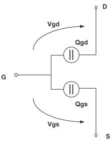
sources, as shown in Fig. 2.1.
Figure 2.1: Gate-channel charge is partitioned into gate-source charge and gate-drain charge.
The charge in the channel with magnitude ofQg is partitioned into gate-source charge
Qgs and gate-drain charge Qgd
Qg =Qgs+Qgd. (2.20)
Here the variables denote magnitudes, and we will write any algebraic signs explicitly as
needed.
The displacement currents can be calculated directly from the voltage-controlled
2.3.2
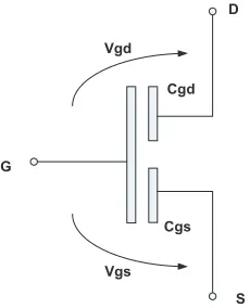
Division by Capacitance
The division-by-capacitance approach is the traditional way to model the gate charge.
In this approach we can write the displacement current as follows
Ig,D =
dQg
dt = ∂Qg
∂Vgs
dVgs
dt + ∂Qg
∂Vgd
dVgd
dt . (2.21)
The two terms are gate-source displacement current and gate-drain displacement current
respectively
Igs,D =
∂Qg
∂Vgs
dVgs
dt (2.22)
and
Igd,D =
∂Qg
∂Vgd
dVgd
dt . (2.23)
The gate-channel capacitance is partitioned into gate-source capacitance and gate-drain
capacitance, as shown in Fig. 2.2.
They are defined as
Cgs =
∂Qg
∂Vgs
(2.24)
Cgd =
∂Qg
∂Vgd
. (2.25)
The gate charge is assumed to be able to be separated into two single-variable functions
Cgs(Vgs) =
∂Qg(Vgs, Vgd)
∂Vgs
= dQgs(Vgs)
dVgs
Cgs Cgd
G
D
S Vgd
Vgs
Figure 2.2: Gate-channel capacitance is partitioned into gate-source capacitance and gate-drain capacitance.
and
Cgd(Vgd) =
∂Qg(Vgs, Vgd)
∂Vgd
= dQgd(Vgd)
dVgd
. (2.27)
The transcapacitances are ignored in the above derivation, resulting in non-conservation
of charge in transient analysis [83].
Charge non-conservation can be fixed by taking into account the transcapacitances
[84]. The terminal transcapacitances are calculated by
Cij =χij
∂Qi
∂Vj
,
χij = 1 f or i=j
χij =−1 f or i6=j ,
(2.28)
where i and j refer to the three terminals, gate, drain and source.
2.3.3
Division by Current
In the division-by-current approach, the division functions fgs(Vgs, Vgd) and fgd(Vgs, Vgd)
cur-rents [82], as shown below
Igs,D =fgs
dQg
dt (2.29)
Igd,D =fgd
dQg
dt . (2.30)
And for all Vgs and Vgd, the division functions should satisfy Kirchoff′s current law
fgs+fgd = 1. (2.31)
The equivalent circuit of the model is shown in Fig. 2.3. The model can be simplified
G
D
S fgsIg
fgdIg
Qg(Vgs,Vgd)
Ig
Ig
Figure 2.3: Gate current is partitioned into gate-source current and gate-drain current.
Qg is a voltage dependent charge source.
by transforming fgd into two sources, and replacing the gate-source current source with
gate capacitance as shown in Fig. 2.4. Fig. 2.5 shows the small-signal equivalent circuit.
Q
g(V
gs,V
gd)
S
G
D
f
gdI
gI
chFigure 2.4: Simplified equivalent circuit of Fig. 2.3. Qg is a voltage dependent charge
source.
characterized from small-signal Y-parameter measurements, andfgd and fgs can then be
determined as introduced in [82].
S
G D
fgdIg
gmVgs
(dQg/dVgd)vgd (dQg/dVgs)vgs
Figure 2.5: Simplified equivalent circuit of Fig. 2.5. Qg is a voltage dependent charge
2.4
Summary
In this chapter prior research on HFET modeling including conduction and displacement
fomulation was summarized in order to place current research in its proper historical
con-text. In the following chapters, the new physics-based compact model will be introduced
Chapter 3
Model Theory Description
3.1
Introduction
In this chapter, the physics-based AlGaN/GaN HFET model is described. The model is
developed, based upon separating the conducting channel of the HFET into a series of
zones, based upon operational physics [3],[19]. The model operates in two modes, triode
and saturation. The transition between the two operations is smooth and dependent
upon device design and operation criteria.
The drain-source conductance current formulation is derived by combining the
phys-ical equations and boundary conditions for each zone. The charge information is then
obtained based on the dc conduction current. The time deviation of the charges in the
HFET contributes to the displacement currents. By properly partitioning the charges
to each electrical terminal, the voltage-controlled charge model can be set up. The
dis-placement currents are calculated based on the division-by-charge approach.
The HFET model is generalized to suit different fabrication processes by introducing
of the HFET in order to control the sharpness of the knee of the I-V characteristics.
The electric field decay region in the drain access is considered for triode operation to
ensure continuity of the terminal characteristics. The pinch off voltage is modified to take
into account different Al mole fractions in the AlGaN barrier layer in the AlGaN/GaN
HFET. Finally, it is necessary to consider channel breakdown in order to accurately
simulate Power Added Efficiency (PAE) at high RF power operation.
The physics-based compact HFET model is verified by comparison of simulated dc
and RF large-signal performance against the measurement and SilvacoTM simulation for
an AlGaN/GaN HFET S-Band amplifier. Good agreements are obtained.
The model is suitable for use in commercial harmonic-balance microwave circuit
simu-lators. It can provide prediction for the dc, small-signal, and large-signal RF performance
for the transistor, given the device geometric structure and design features, material
composition parameters, and dc and RF operating conditions. The model does not
re-quire extensive parameter extraction to determine model element values, as commonly
employed for traditional equivalent-circuit based transistor models. It permits the
co-design and optimization of HFETs in an MMIC environment, which will enhance and
speed integrated circuit development.
The model description is presented in Section 3.2. The physical equations dominated
in each zone is described in Section 3.3, followed by the displacement current in Section
3.2
Model Discription
3.2.1
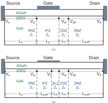
Zone Model of the AlGaN/GaN HFET
The model is formulated based upon separating the conducting channel of the HFET
into a series of five zones. Equations for each zone can be set up according to the physics
dominated, and the I-V characteristics can be obtained.The basic structure for an HFET
is shown in Fig. 3.1.
FM
Lg Ld
Ls
P0vsat , Enss, npiezo
Vd Vg
Vs
HGaN , EgGaN , tGaN FAlGaN , Alx, tAlGaN , Nox
T W
Bvds, Rdsbk, Bkdslp
FM
Lg Ld
Ls
P0vsat , Enss, npiezo
Vd Vg
Vs
HGaN , EgGaN , tGaN FAlGaN , Alx, tAlGaN , Nox
T W
Bvds, Rdsbk, Bkdslp
Figure 3.1: Schematic cross-section of a basic AlGaN/GaN HFET structure, showing the physical parameters of the NCSU HFET model. Four parameters describe layout:
W, Ls, L −g, Ld. Four parameters describe the barrier layer: χAlGaN, Alx, tAlGaN,
nox. Seven parameters describe the GaN buffer: εGaN, EgGaN, tGaN for the GaN itself.
Three parameters for electron transport in the GaN: µ0, vsat,β. Two parameters for its
interface with AlGaN: nss,npiezo. The gate metal is characterized by its electron affinity
χM.
The model operates in two modes, triode and saturation. The transition between the
two modes is smooth and dependent upon device design and operation criteria. Fig. 3.2
shows the salient features of the zone model in its two operating modes. The typical
path from source to drain. This defines the x-y plane, where x is measured from the source electrode and y is measured down from the AlGaN/GaN interface.
For each operating mode, the path between source and drain is segmented into a
few contiguous intervals. In each interval, the physical operation is determined by
two-dimensional numerical simulations and this information is used to develop an analytic
physical model for that particular zone. The 2-D simulations reveal the fundamental
operation of each zone and permit the simplified analytic physical model to be derived.
At the boundaries between adjacent zone intervals, the physical operation changes and the
zones are interfaced by enforcing continuity of the electric potential values and derivatives.
Associated with each interval, we define its zone as the interval itself, initialization of
the distance, potential, and electric field x, V, E. We also define a rule for terminating the interval, and a sequence of operations to compute x, V, E at the end-point and within it, as appropriate.
When the HFET is in triode operation, it can be modeled with four zones. In
sat-urated operation, the model requires five zones. For each operating mode, the terminal
characteristics of the device must be consistent with a simultaneous solution of all the
zones that exist in that mode.
Fortunately, it is possible to compute this simultaneous solution efficiently by setting
up equations for the zones from left to right in sequence, as we will now show. Each
zone is solved in three steps. First, the distance, potential, and electric field parameters
x, V, E are initialized at its left-hand boundary by applying its left-hand initialization rule to the final value of the triple from the preceding zone. Second, the nominal model
Source
Drain
GaNGate
AlGaNV
si 2DEGV
sV
diV
dSNZ Z1 IFZ Z2 DNZ Z5
V
d0 CDZ Z4Lg
L
d,effLs
L
4(a)
Source
Drain
GaNGate
AlGaNV
si 2DEGV
sV
diV
dSNZ Z1 IFZ Z2 DNZ Z5
V
d0 CDZ Z4Lg,eff
L
d,effL
sL4
V
cSLZ Z3
L
3(b)
Figure 3.2: Cross-section of HFET model in (a) triode operation which has four phys-ical zones, and (b) saturated operation which has 5 physphys-ical zones. The voltages at the boundaries between zones are labeled. Except for Z3, the dotted line indicates the electron path in the 2DEG just below the AlGaN/GaN interface. In Z3, the 2DEG is disrupted and the electrons disperse away from the interface to form a net space charge in the GaN.
In either of the two operating modes, the terminal characteristics can be qualitatively
related to the physics of each zone. At zero drain-to-source bias Vds = 0, the channel
consists of three zones, the source and drain access regions and the region beneath the
gate. We denote the source and drain access regions as the source neutral zone (SNZ,
Coulombic neutrality which results from the approximate equality of the sheet charge
density of the 2DEG in these two regions and the polarization charge density. We denote
the region beneath the gate as the intrinsic FET zone (IFZ, or Z2).
For positive Vds, a charge deficit zone (CDZ, or Z4) forms in the drain access region
close to the gate edge. The positive net charge in this partially-depleted region (Z4)
smoothly reduces the magnitude of the electric field, in accordance with Poisson′s
equa-tion. In the triode mode, the length of the zone Z4 is short and the voltage drop across
it is typically less than a volt, but it is required for continuity of Vds at the transition
between the triode mode and saturated operation atVds =Vds,sat. At fixed gate bias, the
length of the CDZ zone increases with drain bias, which reduces the length of the DNZ
zone, since the sum of their lengths is constrained to equal the gate-to-drain distanceLd.
For saturated operation, Vds > Vds,sat. Electrically in the Vds-Ids plane, the transition
between the triode mode and saturated operation occurs at the knee of the I-V curve,
where the slope of the curve flattens. Physically, saturated operation begins when the
magnitude of the longitudinal electric field in the channel at the drain-side gate edge,
denoted asEdi, first exceeds the critical field,Ec, which effectively pinches the 2DEG off
by flat-banding the quantum well.
With increasing Vds, the electric field (Edi > Ec) at the drain-side edge of the gate
continues to increase and the location whereE first exceeds Ec moves toward the source.
Under the gate, we denote the location whereE =Ec asxc and the voltage there asVc. In
the regionxc < x < Ls+Lg, electrons are repelled away from the AlGaN/GaN interface
to form the velocity-saturated space-charge limited zone (SLZ, or Z3). This SLZ extends
longitudinally to the gate edge and typically extends down to the substrate because the
gate repels electrons when Vgt < V, so that the Gradual Channel Approximation (GCA)
At fixed gate bias, with increasing Vds, the length of the SLZ zone increases, which
reduces the length of the IFZ zone under the gate since the sum of their lengths is
constrained to be Lg. In the drain access region, the length of the CDZ zone increases
simultaneously with increasing Vds as mentioned previously.
The Gradual Channel Approximation (GCA) is readily adapted to zones Z1, Z2, and
Z5. In zone Z3, the GCA fails because the carrier trajectories are not one-dimensional
as discussed above. In zone Z4, the 2DEG has re-established itself, but the sheet charge
density of the 2DEG is insufficient to neutralize the fixed polarization sheet charge, and
electron velocity in this 2DEG is effectively saturated. This Charge Deficit Zone (or zone
Z4) can affect device operation over part of the RF cycle.
In zone Z4, the 2DEG is stable but is incompletely filled. The length of zone Z4 is
approximately proportional to the difference Edi−Ec, but Edi increases with Ids until
Edi ≥ EBD when impact ionization in the channel produces unacceptable breakdown
effects at the device terminals. In GaN, the breakdown electric field EBD ≫Ec is about
two orders of magnitude larger than the electric field Ec at which velocity saturation
begins. Therefore, the maximum length of this region is proportional toEBD−Ec which
is exceptionally large for GaN. Electrons enter zone Z4 with their velocity saturated and
the transistor effect of the gate region limits the current almost independently of the
local electric field, even when it is two orders of magnitude larger than Ec, as it can be
in GaN before it breakdown occurs at very highVds. This combined effect keeps zone Z4
partially depleted, so that at fixed gate bias, the voltage dropped across zone Z4 increases
approximately quadratically with its length, which adjusts itself to gradually reduce E
fromEdi toEs, where the field-dependent mobility of the electrons is sufficiently high to
3.2.2
Generalized Velocity-Field Relationship for Carrier
Elec-trons
Theoretical investigations of electron dynamics using Monte Carlo techniques have
de-termined velocity-field characteristics associated with GaN materials. These theoretical
simulations show that the electron drift velocity initially increases with the applied
elec-tric field but reaches a peak value, after which it gradually decreases to a saturated value
at a high electric field [85]. The peak value decreases with increasing doping
concen-tration and temperature [86]. Some v-E relationships for electron transport in a 2DEG
for the AlGaN/GaN structure have been reported [85] [87]. However, no evidence of
a velocity overshoot is apparent in the terminal characteristics of devices that we have
considered.
In fact, an equilibrium v-E characteristic has proved adequate to accurately simulate experimental results and we find that (3.1) accurately simulates the dc and RF currents
that flow in experimental AlGaN/GaN HFETs
v(E) = µ0E 1 +EE
c
β1/β, (3.1)
where β controls the curvature of the knee of the v-E curve, and where
E =−E(x) = dV
dx (3.2)
is defined as the negative of the usual longitudinal electric field and we regard it as a
function of distance from the source electrode.
important in calculating the knee region of the dc current-voltage relationship for the
device. We have found that the same v-E model (3.1) accurately simulates both the dc and large-signal RF operation. Consequently, we have chosen (3.1) for the velocity-field
relationship because its transition is smooth but adjustable.
In (3.1),µ0 is the low-field electron mobility, which is a function of lattice temperature and doping concentration, and relates the saturation velocity and the critical electric field
by the relation
vsat = 2−1/βµ0Ec, (3.3)
wherevsat is the temperature-dependent asymptotic saturated velocity. Ec is the critical
electric field marking the onset of the high-field region
Ec = 21/βvsat/µ0, (3.4)
and β controls the curvature of the knee of the v-E curve. From experimental data, this curvature parameter varies over the interval 1≤ β ≤2, so that the critical electric field depends on β as well as vsat. The values of the µ0,vsat,β parameters can be determined
by adjusting the estimated physical-based values so that the simulated terminal I-V
characteristics matches the measured I-V data for an HFET.
Fig. 3.3a shows how β controls the curvature of the knee of (3.1) without changing the low-field and high-field regions of the v-E model. In the limit of large β, this v-E
10−1 100 101 102 103 105
106 107
E−field kV/cm
Ve
lo
ci
ty
cm/
s
vlin vsat beta=0.8 beta=2 beta=100
(a)
10−1 100 101 102 103
105 106 107
E−field (kV/cm)
Ve
lo
ci
ty
(cm/
s)
two−field model
v−E used in our model, beta=1
(b)
Figure 3.3: Plotting v-E relationship in (a) for various β values, and in (b) comparing (3.1) (red) with that of the two-field model (blue).
We estimate the saturated velocityvsat, the low-field mobilityµ0, and the rate of
tran-sition from v ≈2−1/βµ
0E tov ≈vsat from simultaneous fits of dc and RF measurements
mobility at low electric field is generally determined from measured Hall mobility data.
This value may be slightly varied in order to accurately simulate the measured dc I-V
data in the linear region in some cases, but does not significantly vary from the Hall
values, and often the measured Hall value is found to produce excellent results.
3.2.3
Pinch Off Voltage
The conducting channel in an AlGaN/GaN HFET is formed from the 2DEG just below
the interface of the AlGaN barrier layer that is grown on a GaN layer. This 2DEG
conducting channel is formed by spontaneous and piezoelectric polarization effects at the
AlGaN/GaN interface [88], [89].
Fig. 3.2 shows the cross-sectional view of an HFET. The sheet charge density of
this 2DEG channel is determined by the aluminum percentage and the thickness of the
AlGaN layer. The sheet charge density can be modulated by the deposition of a gate
electrode on the AlGaN surface and by the electric voltageVg that is applied to the gate
electrode. When Vg is sufficiently negative, the channel vanishes everywhere under the
gate, and in particular at the source-side edge of the gate, which determines the pinch off
voltageVth of the AlGaN/GaN HFET. The pinch-off voltage is conventionally written as
Vth(m) = Φth(m)−∆Ec(m)−
qNDd2d
2ε(m) −
σ(m)
ε(m)deff, (3.5)
which a function of mole fraction m of aluminum in the AlmGa1−mN, and Vth also
de-pends on the effective thickness deff of the AlGaN barrier, its Schottky barrier height
Φth(m), its electric permittivityε(m), and its dopingND, as well as the conduction band
polarization sheet charge σ(m). In (3.5), the dielectric constant is expressed as [85]
ε(AlmGa1−mN) =ε(GaN)−1.2m. (3.6)
The band gap of AlGaN [90, 91] is
Eg(AlmGa1−mN) =Eg(GaN) + 2.32m+ 0.0796m(1−m), (3.7)
and the Schottky barrier is expressed as [92]
Φ = 0.91 + 2.44m, (3.8)
and the band offset is given by the expression
∆Ec = 0.7 (Eg(AlmGa1−mN)−Eg(GaN)). (3.9)
The values of the parameters for pinch off are listed in Table 3.1. In practical
simu-lation, the parameters have been adjusted slightly to get better fitting.
Table 3.1: Energy band parameters.
Parameter Unit Value Description
ε(GaN) F/m 9.7e−11a Static dielectric constant of GaN
Eg(GaN) eV 3.52a Band gap of GaN
χm eV 4.3 Affinity of metal
χAlGaN eV 3.8 Affinity of AlGaN
3.3
Physics of the zones
3.3.1
Zones Z1 and Z5, Source Neutral Zone (SNZ)
In zones Z1 and Z5, the current at location x is conducted by the 2DEG, but for steady state operation, I(x) = Ids cannot depend on x. According to 1-D current density
equation, we have
Ids =W qn(x)v(x) +qW Dn
dn(x)
dx , (3.10)
where Ids is the drain current, W is the gate width, q is the fundamental charge, n(x)
is the local electron density of the 2DEG, and v(x) is the electron velocity at position x
along the channel. Dn is the electron diffusion coefficient expressed as
Dn=Vtµn, (3.11)
where
Vt=
kBT
q . (3.12)
In order to establish equations for each zone, the standard approximations are made:
We assume quasi-static operation; The Einstein′s relationship is valid; and the magnetic
field is neglected.
In the first, we consider the drift current induced by the electric field. The diffusion
reduced to
Ids =W qn(x)v(x). (3.13)
In the source access region, n(x) is fixed as
n(x) =nss=
σ(m)
q (3.14)
to neutralize σ(m), so that (3.1) and (3.12) imply that
E(x) = EcIds
Imaxβ −Idsβ
1/β ≡Es (3.15)
is constant with respect to x, where Es is the value of that constant at a given Ids, and
Imax=W qnssvsat (3.16)
is a convenient scale factor for Ids for a given HFET.
The potential profile in zone Z1 is expressed as
V(x) =
Z x
0
Esdx=Esx. (3.17)
The voltage at the source-side gate edge can be expressed as
Vsi =EsLs (3.18)
neutral zone of the HFET. In contrast to the fixed length of zone Z1, the length of
zone Z5 is state dependent. Zone Z5 begins when the lateral field in zone Z4 has finally
diminished to E(x) =Es, which terminates zone Z4. Within both the Source and Drain
Neutral Zones, electron transport is identical and Es sets the drift velocityv(Es) in both
zones Z1 and Z5.
The source and drain access regions, zones Z1 and Z5, introduce an extrinsic
resis-tance to the intrinsic HFET and will affect the performance of the HFETs. It has been
previously shown that under high current operation and large-signal RF drive, these
re-sistances become non-linear as space-charge-limited (SCL) current transport conditions
are approached [18]. Both the source and drain resistances become non-linear and
in-crease with channel current. The effect is most apparent in the source region since the
voltage drop across the source access region subtracts directly from the applied Vg and
limits the drain current of the HFET considerably beforeIds increases toIds,sat. The drop
across the drain access region lowers the slope of Ids in the triode region and increases
the drain bias required to achieve Ids,sat.
In power microwave applications, using a constant resistance for either will typically
overestimate the drain current at the upper left limit of the dynamic load line and with
it, the output power. From (3.15) and the length Ls of the source access region, we find
Rs=
VSNZ
Ids
= EcLs
Imaxβ −Idsβ
1/β, (3.19)
where VSNZ is the voltage drop across the SNZ zone. The drain access region can be
treated similarly but both zones Z4 and Z5 must be considered. Fig. 3.4 shows the
nonlinear source resistance as a function of the chancel conductance current with a source
0 0.1 0.2 0.3 0.4 0.5 0
5 10 15 20 25 30
Ids (A)
R
s
(o
h
ms)
beta=2, 1.5, 1.2
Figure 3.4: Rs as a function of the conductance current with different beta. The values
of β are 2, 1.5 and 1.2 respectively. The length of the source access region is 1.2um.
3.3.2
Zone Z2, Intrinsic FET Zone (IFZ)
At the source-side gate edge, electrons leave zone Z1 and enter zone Z2. In zone Z1,
the voltage on the upper AlGaN surface follows the voltage V(x) of the 2DEG at the AlGaN/GaN interface. In zone Z2, however, the gate electrode holds the surface voltage
atVg.
According to Poisson′s equation and the GCA, we write the electron sheet density at
position x
asn(x) = Ceff
q (Vgt−V(x)). (3.20)
It′s expressed in terms of the effective gate voltage
and the effective gate-channel capacitance per unit area
Ceff =ε(m)/deff, (3.22)
where deff is the effective thickness of the AlmGa1−mN barrier layer.
Electrons in zone Z2 drift toward the drain because V(x) increases with x in the channel, but this drift cannot persist past where V(x) has risen enough to exceed Vgt.
Following the GCA, we substitute (3.1) (3.2) and (3.20) into (3.13), reorganize and
integrate the obtained equation fromLs tox, we get
(x−Ls)Ids = Z V(x)
Vsi
(W u0Ceff(Vgt−V ′
))β −(Ids
Ec
)β
1/β
dV′. (3.23)
In triode operation, the channel fills the entire gate region. Replacing xwithLg+Ls,
and V(x) with Vdi, we find
LgIds = Z Vdi
Vsi
(W u0Ceff(Vgt−V))β −(
Ids
Ec
)β 1/β
dV , (3.24)
whereLg is the physical gate length. The lower limit of the integralVsi is given by (3.18).
The upper limit of the integralVdi is expressed as
Vdi=Vd−
Ec(Ld−L4)Ids
Imaxβ −Idsβ
1/β −
1 2L
2
4k4, (3.25)
which is the voltage at the drain-side edge of the gate in triode operation, and Ld and
L4 are the lengths of drain access and zone Z4. The derivation details will be presented in the following sections.
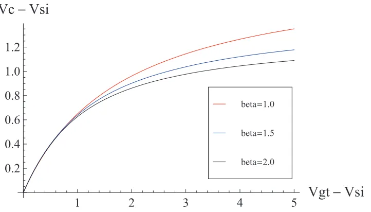
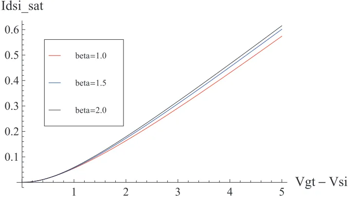
beforex=Ls+Lg, then the device is in saturated operation. In triode operation, zone Z3
does not affect the parametersx,V,E, because its lengthLs+Lg−xc = 0 vanishes, zero
voltage is dropped across the zone, and the electric field does not change. In saturation,
zone Z3 is significant because Ls+Lg−xc >0 when Ids > Ids,sat.
In saturated operation, Vdi and Edi are still defined at the drain-side gate edge, but
(3.24) is not valid there because the longitudinal electric field exceeds Ec before exiting
the gate region, so that Edi > Ec and Vdi > Vc. In this case, the length of zone Z2,Lg,eff,
is Lg subtracted by the length of zone Z3, and we write
Lg,effIds = Z Vc
Vsi
(W u0Ceff(Vgt−V))β−(
Ids
Ec
)β
1/β
dV, (3.26)
where
Vc =Vgt−
Ids
W Ceffvsat
. (3.27)
The transition of terminal characteristics between the triode mode and saturated
operation occurs when the drain current is high enough to make Vdi = Vc and Edi =Ec
at the gate edge. This Ids,sat is determined by using (3.27) for the upper limit of (3.24)
and solving
LgIds,sat = Z Vc
Vsi
(W u0Ceff(Vgt−V))β−(
Ids,sat
Ec
)β
1/β
dV (3.28)
3.3.3
Zone Z3, Space-Charge Limited Zone (SLZ)
The SLZ zone only occurs when the device enters saturation. We approximate the
one-dimensional Poisson′s equation as
dE dx =
qn(x)
εt(x) =
Ids
εW v(x)t(x) =k3(x), (3.29)
wheret(x) andv(x) is the thickness and velocity of electrons at positionxin the channel in zone Z3. The electron velocity v(x) is approximated as vsat since the electric field in
this zone is greater than the critical field. As determined from two-dimensional finite
element simulations, we assume
n(x)
nss ≈
αt(x) tGaN
, (3.30)
where α is an adjustable parameter. Also from the current continuity equation we have
Ids
Imax
= n(x)
nss
. (3.31)
So that we can define the average electric field derivative as
k3 =
∂E ∂x
=
Imax
εW v(x)tGaN
≈α qnss εtGaN
. (3.32)
Integrating Poisson′s equation once from x
c tox yields
E(x) =Ec + Z x
xc
∂E
and a second integration yields
V(x) =Vc+
Z Z x
xc
∂E
∂xdxdx. (3.34)
Then at the boundary between the zones Z3 and Z4, the electric field and voltage can
be expressed as
Edi=Ec+ Z Lg
Lg−L3
∂E
∂xdx (3.35)
and
Vdi =Vc+
Z Z Lg
Lg−L3
∂E
∂xdxdx. (3.36)
3.3.4
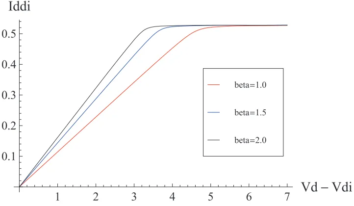
Zone Z4, Charge Deficit Zone (CDZ)
Zone Z4 occurs in both triode and saturated operation when Edi > Ec as defined by
(3.4). Since the surface voltage in zone Z4 is not clamped by the gate electrode, it rises
with the channel potential V(x). The 1-D Poisson′s equation can be expressed as
dE dx =
qn(x)
εt(x) −
Ids
εW v(x)t(x) =k4, (3.37)
which can be used to obtain the length of zone Z4
L4 =
Edi−Es
k4
. (3.38)
conditions lead to the following electric field and potential profile
E(x) =Edi+ Z x
Lg
∂E
∂xdx (3.39)
and
V(x) =Vdi+
Z Z x
Lg
∂E
∂xdxdx. (3.40)
Then at the boundary between zones Z4 and Z5
Ed0 =Edi+
Z Lg+L4
Lg
∂E
∂xdx (3.41)
and
Vd0 =Vdi+
Z Z Lg+L4
Lg
∂E
∂xdxdx. (3.42)
3.3.5
Zone Z5, Drain Neutral Zone (DNZ)
Within zone Z5, the nominal electron physics are identical to that in zone Z1 but the
zone length varies dynamically and satisfies different boundary conditions. As in zone
Z1, overall charge neutrality prevails in zone Z5 and the current is described by (3.13)
and (3.15), so the lateral electric field in zone Z5 is constant and coincides with Es in
zone Z1. In the preceding zone Z4, E(x) > Es but the electric field continuously varies
from magnitude Edi toEs.
In zone Z5 the electron transport model is similar as in zone Z1, the SNZ, but the
Z5 begins when the lateral electric field in zone Z4 is reduced to its value in zone Z1.
The potential profile in zone Z5 is
V(x) =Vd0+Es(x−Ls−Lg −L4). (3.43)
The voltage at the drain terminal is
Vd =Vd0+Es(Ld−L4). (3.44)
It may be possible to fabricate an HFET with sufficiently short drain access region
and to bias it at high enough drain voltage to deplete the entire drain access region, but
we have not observed this in any device we have considered. Currently we treat this
possibility as an error condition.
We can include zone Z3 in the sum
j=5
X
j=1
(∆V)Zj (3.45)
over all five zones of voltage increments for each zone to get the following expression
Vds(Vgt, Ids) = j=5
X
j=1
(∆V)Zj. (3.46)
In the triode mode, we can define (∆V)Z3 = 0 in the same sum. To re-express this result as the controlled current source Ids(Vgt, Vds) for given Vgt and Vds, we invert the