Broadband Waveguide-Fed 8-by-1 Gap-Coupled Microstrip Antenna
Array for 60-GHz Short-Range Point-to-Point Wireless
Communications
Chaouki Hannachi*, Djerafi Tarek, and Serioja O. Tatu
Abstract—In this paper, a 60-GHz broadband 8-by-1 gap-coupled microstrip antenna array is presented and experimentally investigated. The proposed antenna array has been implemented using a Miniature Hybrid Microwave Integrated Circuits (MHMIC) fabrication process on a thin ceramic substrate with
εr = 9.9 and h = 127µm. For a comprehensive characterization and to accurately evaluate losses, as
well as manufacturing tolerances, the proposed antenna array structure has been implemented using two different feeding techniques. The first one adopts a grounded broadband via-hole less transition from coplanar to microstrip line (GCPW-to-MS), while the second one has involved a broadband waveguide (WR12) to microstrip transition, based on a ridged waveguide concept. The obtained results have demonstrated that the proposed gap-coupled array configuration provides an improved bandwidth (4.56%) and an enhanced gain (11.8 dBi), while maintaining a lower side-lobe level (13.4 dB). These outstanding performances make the proposed WR12 gap-coupled array structure a potential candidate for the future emerging 60-GHz short-range point-to-point wireless communication systems.
1. INTRODUCTION
In the last few decades, the trend in wireless communication systems has been to develop low cost, small size, and low-profile antennas that provide high performance over a large spectrum of frequency bands [1, 2]. In this context, much attention has been focused into the design of microstrip patch antennas due to their several advantages. In fact, they are distinguished by a simple geometry, low fabrication complexity and ease of integration with microwave and millimeter-wave integrated circuits (MMIC). Despite the many advantages, patch antennas have some drawbacks. One of the main limitations is their inherently narrowband performance due to its resonant nature (bandwidth is typically on the order of a few percent) [3].
Recently, various techniques have been employed to improve the bandwidth, including stack layers, defected ground structures, square slot techniques, and gap-coupled multiple resonators concepts [1, 4– 6]. In the last approach, only single microstrip patch antenna is fed, and other patches are parasitically coupled. The coupling between the parasitic patch and resonating patch is achieved by introducing small gap between them. The typical configuration involves one or multiple parasitic patches having almost identical size, which are placed along the fed patch to increase the operational bandwidth [7–9]. Gap-coupled microstrip antennas have been the subject of extensive researches over the last few years. Nevertheless, most of the reported configurations in the literature have paid more attention to low frequency antenna structures adopting various feeding techniques, such as microstrip line feed, coaxial probe feed, aperture and proximity coupled feed [10–13]. However, millimeter-wave gap-coupled
Received 30 November 2018, Accepted 16 January 2019, Scheduled 20 March 2019
* Corresponding author: Chaouki Hannachi ([email protected]).
antenna structures based on rectangular waveguide fed for specific applications have not been addressed in the literature.
In this paper, a 60-GHz 8-by-1 gap-coupled microstrip antenna array is designed, fabricated, and investigated. To ensure a detailed characterization, the proposed gap-coupled array structure has been validated using two different feeding techniques. The first one involves a grounded broadband via-hole less transition from coplanar to microstrip line (GCPW-to-MS), whereas the second technique employs a broadband waveguide (WR12) to microstrip transition, based on a ridged waveguide concept. Both gap-coupled antenna array prototypes are designed on a thin-film ceramic substrate (εr= 9.9,h= 127µm),
using an MHMIC (Miniature Hybrid Microwave Integrated Circuits) fabrication process.
In the proposed configuration, eight optimized isosceles trapezoid patches are introduced at a proper distance from each driven element to maintain an appropriate coupling level. However, to investigate the size effect of the parasitic elements on the proposed gap-coupled structure, parametric studies were conducted to enable an optimized size and a precise input impedance matching. The obtained performances in terms of operational bandwidth, realized gain, and side-lobe level clearly confirm the potential of the proposed gap-coupled array structure to be a suitable candidate for the future emerging 60-GHz short-range point-to-point wireless communication systems.
2. ANTENNA DESIGN, FABRICATION, AND CHARACTERIZATION 2.1. Design of the 8-by-1 Gap-Coupled Antenna Array
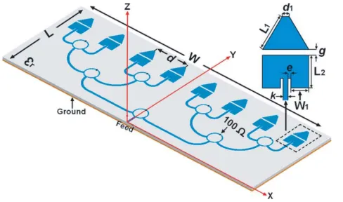
The proposed 8-by-1 gap-coupled antenna array has been designed on a thin-film ceramic substrate with dielectric constant εr = 9.9 and heighth = 127µm. The MHMIC (Miniature Hybrid Microwave
Integrated Circuits) fabrication process was employed for the implementation of the gap-coupled antenna array prototype. The structure of the proposed antenna array with its geometrical parameters is shown in Figure 1. It consists of eight gap-coupled patch elements spaced approximately 0.55λo
(λo = 5 mm), and a parallel feed network that is composed of seven rounded shape Wilkinson power
dividers/combiners, along with the 50 Ω transmission lines. The adopted design approach uses the gap-coupling technique in which an optimized coupling level from the driven to the parasitic element is achieved. This concept significantly enhances the operational bandwidth and may allow up to 3 dB more gain. As parasitic elements, the isosceles trapezoid patches are selected and optimized to reduce the effect of mutual coupling between antenna elements and reach a higher resonant frequency. The optimized geometrical parameters of the antenna array structure are: W = 18.310, L = 7.805,
W1= 0.419, L1 = 0.888,L2 = 0.759, d= 2.5, d1 = 0.152, e= 0.069, g= 0.10,k= 0.127, with all units
being millimeters.
A parametric study of the antenna array is performed to analyze and understand the dimensional parameters effects of the parasitic element on the resonant frequency, and accordingly the antenna array
Figure 1. The 8-by-1 gap-coupled antenna array design with the geometrical parameters.
frequency bandwidth. In this study we introduce three geometric shapes, in addition to the parasitic element shape already employed. As illustrated in Figure 2, these shapes include a rectangle (in 4,
x = 2λg/3 = 1.06 mm), an isosceles trapezoid (in 3, x = λg/3 = 0.53 mm), and a triangle (in 1,
x= 0 mm). The obtainedS-parameters results within the considered frequency range clearly show that the selected parasitic element (in 2,x=λg/10 = 0.15 mm) for the proposed array design provides a large
bandwidth and an optimal coupling while reaching a second higher resonant frequency, at 62.2 GHz. It is noteworthy that based on same parametric study we have demonstrated that the optimized gap thickness between driven and parasitic elements is g = 0.10 mm. This value allows an accurate input impedance matching over the considered frequency band.
2.2. Design of the Millimeter-Wave Microstrip Line to Waveguide (WR12) Transition
A rectangular WR12 waveguide to microstrip line transition has been designed on the same thin-film high-permittivity ceramic substrate to feed the gap-coupled antenna array. In the proposed structure a linear ridge section having approximately a length of λg was introduced inside the rectangular
WR12 waveguide to allow impedance matching between microstrip line and the rectangular WR12 waveguide [14–16]. Furthermore, this enables a gradual conversion of electric field mode, from the fundamental TE10 mode in the rectangular waveguide to the microstrip line quasi-TEM mode. The
proposed transition structure, including its geometrical parameters, and the fabricated prototype are shown in Figures 3(a) and (b), respectively. The optimized transition dimensions are as follows:
H = 1.422, W1 = 3.098, L = 9.123, L1 = 7.067, L2 = 7.811, g = 0.739, W = 3.721, s = 0.439,
f = 0.254, d= 0.127, with all units being millimeters.
The transition design parameters are initially calculated theoretically and subsequently have been optimized using Ansoft High Frequency Structure Simulator (HFSS), based on highly accurate finite element method (FEM) [17]. This full-wave electromagnetic (EM) software provides high level optimization capabilities and accurate assessment of electromagnetic behaviors.
Furthermore, considering the ceramic substrate fragility (h = 127µm, and thin gold layer metallization of 1µm), some arrangements were considered during the mechanical part manufacturing. However, a limit for the fixing screws is set to avoid substrate damaging. In addition, the ceramic substrate was firmly embedded in the metal block to ensure a good ground contact, while providing protection against vibration and shock.
The simulated and measured S-parameter results of the fabricated back-to-back transition are shown in Figure 4. The obtained results are in good agreement and show a return loss better than
(a) (b)
Figure 3. The geometrical parameters of the designed waveguide (WR12) to microstrip transition in (a), and the photograph of the fabricated prototype in (b).
15 dB within the frequency range of 60 to 70 GHz. However, a frequency shift response about 4.8% between simulation and measurement has occurred. This is probably due to the uncertainty in substrate thickness, and permittivity deviation frequently happens at millimeter-wave bands. The measured insertion loss over the same frequency band varies from 1.5 to 1.9 dB.
It should be noted that the relatively high losses are mainly related to metal losses (0.0025 dB/cm), the surface resistivity on the waveguide walls (0.063 Ohms/sq), and particularly the losses due to tolerances in manufacturing process and mechanical assembly.
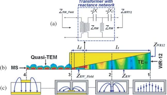
The equivalent circuit model of the junction at the metal ridge and substrate, and the simulated electrical field inside transition with the electric field intensity distributions at the main cross-sections (1–4) are illustrated in Figures 5(a), (b) and (c), respectively. As can be seen, the electrical field is uniformly distributed along the rectangular waveguide, the transition, and the microstrip line while ensuring transformation from TE10 mode (Waveguide) to quasi-TEM mode (Microstrip line).
The discontinuity at the substrate-air junction is modeled using lumped-element components. In this respect, simple mechanism is introduced to remove the imaginary portion created by the junction effect. Our approach is therefore to add dielectric transmission line having an impedance ZRW Field
and length of ld = 0.3 mm, behind a ridge contact. This would enable the reflection coefficient Γ to
rotate toward purely resistive loads on the Smith chart. The linear ridge taper length, lt = 4.07 mm,
is introduced for impedance matching purpose of the two purely resistive impedances,ZRW andZWR12
(see Figures 5(a) and (b)).
(a)
(b)
(c)
Figure 5. The metal ridge/substrate junction equivalent circuit in (a), simulated electrical field inside transition in (b), and the electric field intensity distributions at the main cross-sections (1–4) in (c).
2.3. Fabrication, Measurement Results, and Discussion
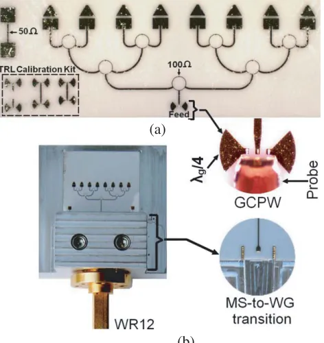
In order to ensure a complete characterization of the proposed 8-by-1 gap-coupled antenna array, a separate prototype is also implemented for on-wafer measurement. In this respect, a grounded broadband via-hole less transition from coplanar to microstrip line (GCPW-to-MS) and a precise on-wafer measurement structure were employed. The on-on-wafer structure is equipped with ground-signal-ground GSG 150µm coplanar probes from Cascade Microtech, as shown in Figure 6(a). Moreover, to ensure an accurate on-wafer S-parameter measurement, a thru-reflect-line (TRL) calibration standard design and resistors test kit to verify integrated 100 Ω per square resistors were also introduced on the same thin-film alumina substrate [18, 19]. Indeed, this further design is very useful since it allows an estimation of metal losses in rectangular waveguide and an assessment of the mechanical assembly tolerances in waveguide (WR12) to microstrip transition.
(a)
(b)
Figure 6. Photograph of the fabricated 8-by-1 gap-coupled antenna array: (a) prototype with grounded coplanar to microstrip line (GCPW-to-MS) transition and, (b) prototype with waveguide (WR12) to microstrip transition.
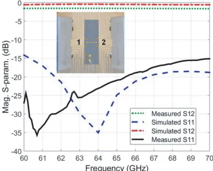
Figure 7. Measured and simulatedS-parameters of the fabricated 8-by-1 gap-coupled antenna array.
E8362B (10 MHz–20 GHz) Vector Network Analyzer, connected with E-band (60–90 GHz) extension modules. It is for this reason that the proposed antenna array has been designed to operate in frequency range of 60 to 65 GHz, and the measurements were carried out from 60 GHz instead of 57 GHz (the starting frequency of unlicensed 60 GHz frequency band). The measurements are compared with the simulations from HFSS software tool in Figure 7, over the frequency range from 60 to 65 GHz. As can be seen, measurements and simulations are in reasonable agreement. They are below −10 dB in the band of 60 GHz to 62.8 GHz, which represents a measured bandwidth of 4.56% at the center frequency of 61.4 GHz. However, the measured S-parameter using waveguide (WR12) to microstrip transition shows a relatively wider bandwidth. This is due to the extra loss added by the waveguide (WR12) to microstrip transition mismatch. Measured frequency shift response about 0.2 GHz (0.3%) is also observed, which is principally due to the tolerances in substrate and fabrication process, as mentioned earlier.
As can be seen, the S-parameter measurement results using coplanar-waveguide-to-microstrip transition show better agreement with simulations. In fact, the thin-film microstrip line losses are not significant, and they have been estimated using on-wafer probing measurement results (the average loss per mm is about 0.05 dB at 61 GHz).
To observe the excitation mechanism, average surface current distributions obtained from HFSS simulation on the conductor for the optimized 8-by-1 gap-coupled antenna array were studied. As can be seen in Figure 8(a), the electrical field is uniformly distributed and coupled from the driven to the parasitic elements, resulting in the excitation of all patches. It is important to note that this coupling is mostly managed by the gap thickness (g) between driven and parasitic elements (see Figure 1).
The simulated and measured radiation patterns at 61 GHz in E-planes are shown in Figure 8(b). As can be observed, the results demonstrate a good concordance, while maintaining high symmetry and a maximum level of radiation at the broadside direction.
(a)
(b)
Figure 8. Simulated surface current distributions on the conductor of the 8-by-1 gap-coupled antenna array at 61 GHz in (a), and E-plane measured and simulated radiation pattern in (b).
Figure 9. Simulated and measured peak gains of the fabricated 8-by-1 gap-coupled antenna array versus frequency.
lobe is about 13.4 dB below the main lobe. Hence, this low side lobe level indicates that the proposed array antenna largely meets the requirements for millimeter-wave short-range point-to-point wireless communications.
The results of the measured and simulated peak gains of the fabricated 8-by-1 gap-coupled antenna array prototype versus frequency are plotted in Figure 9. Reasonable agreement between simulation and measurement is achieved with more than 10 dB of measured gain over the frequency range of 60 to 62.5 GHz. The maximum measured peak is 11.8 dB at 61 GHz (simulated 13.5 dB). The difference between the simulated and measured gains varies from 1 to 2 dB over the considered frequency range from 60 to 62.5 GHz (in the −10 dB return loss bandwidth). These losses remain acceptable, and, as mentioned above, they are mostly due to the waveguide (WR12) to microstrip transition and manufacturing tolerances.
3. CONCLUSION
Integrated Circuits) fabrication process. The proposed antenna array configuration has demonstrated a broadband operation (about 4.56% bandwidth with respect to central frequency) and a peak gain of about 11.8 dB at 61 GHz, while keeping a low side-lobe level (13.4 dB). The performances achieved make the proposed WR12 gap-coupled antenna array a highly suitable candidate for the future 60-GHz short-range indoor point-to-point wireless communication systems.
ACKNOWLEDGMENT
The authors would like to acknowledge the Natural Sciences and Engineering Research Council of Canada (NSERC) for its generous research support and the “Centre for Systems, Technologies and Applications for Radiofrequency and Communication” (STARaCom) of Montr´eal, funded by the “Fonds de recherche du Quebec-Natures et technologies” (FRQNT), for the MHMICs fabrication.
REFERENCES
1. Balanis, C. A., Antenna Theory Analysis and Design, 3rd Edition, Wiley, New York, NY, USA, 2011.
2. Kumar, G. and K. P. Ray,Broadband Microstrip Antennas, Artech House, Boston, MA, USA, 2003. 3. Hannachi, C. and S. O. Tatu, “Performance comparison of 60 GHz printed patch antennas with different geometrical shapes using miniature hybrid microwave integrated circuits technology,”IET Microwaves, Antennas &Propagation, Vol. 11, No. 1, 106–112, Jan. 2017.
4. Fan, S. T., Y. Z. Yin, B. Lee, W. Hu, and X. Yang, “Bandwidth enhancement of a printed slot antenna with a pair of parasitic patches,” IEEE Antennas and Wireless Propag. Lett., Vol. 11, 1230–1233, 2012.
5. Wong, H., K. K. So, and X. Gao, “Bandwidth enhancement of a monopolar patch antenna with V-shaped slot for car-to-car and WLAN communications,” IEEE Trans. Veh. Technol., Vol. 65, No. 3, 1130–1136, Mar. 2016.
6. Sallam, M. O., S. M. Kandil, V. Volski, G. A. E. Vandenbosch, and E. A. Soliman, “Wideband CPW-fed flexible bow-tie slot antenna for WLAN/WiMAX systems,” IEEE Transactions on Antennas and Propagation, Vol. 65, No. 8, 4274–4277, Aug. 2017.
7. Aanandan, C. K., P. Mohanan, and K. G. Nair, “Broad-band gap coupled microstrip antenna,” IEEE Transactions on Antennas and Propagation, Vol. 38, No. 10, 1581–1586, 1990.
8. Wood, C., “Improved bandwidth of microstrip antennas using parasitic elements,” IEE Proc. — Microw. Antennas Propag., Vol. 127, No. 4, 231–234, Aug. 1980.
9. Kumar, G. and K. Gupta, “Broad-band microstrip antennas using additional resonators gap-coupled to the radiating edges,”IEEE Transactions on Antennas and Propagation, Vol. 32, No. 12, 1375–1379, Dec. 1984.
10. Deshmukh, A. A., S. Nagarbowdi, P. A. Kadam, and A. A. Odhekar, “Broadband gap-coupled isosceles triangular microstrip antennas,” 2017 International Conference on Emerging Trends & Innovation in ICT (ICEI), 67–72, Pune, 2017.
11. Nirate, S., R. M. Yadahalli, K. K. Usha, R. M. Vani, and P. V. Hunagund, “Wideband gap-coupled suspended rectangular microstrip antenna,” 2008 International Conference on Recent Advances in Microwave Theory and Applications, 833–835, Jaipur, 2008.
12. Bhalekar, P., L. K. Ragha, and R. Gupta, “Wideband gap coupled microstrip antenna using RIS and RIS cavity resonator,” 2017 2nd IEEE International Conference on Recent Trends in Electronics, Information & Communication Technology (RTEICT), 1291–1295, Bangalore, 2017.
13. Rathod, S. M., R. N. Awale, K. P. Ray, and A. D. Chaudhari, “A compact gap coupled half-hexagonal microstrip antenna with improved bandwidth,” 2017 IEEE Applied Electromagnetics Conference (AEMC), 1–2, Aurangabad, 2017.
15. Hannachi, C., T. Djerafi, and S. O. Tatu, “Broadband E-band WR12 to microstrip line transition using a ridge structure on high-permittivity thin-film material,” IEEE Microwave and Wireless Components Letters, Vol. 28, No. 7, 552–554, July 2018.
16. Nasr, M. A. and A. A. Kishk, “Wideband inline coaxial to ridge waveguide transition with tuning capability for ridge gap waveguide,” IEEE Transactions on Microwave Theory and Techniques, Vol. 66, No. 6, 2757–2766, 2018.
17. Corporation, A., Ansoft High Frequency Structure Simulation (HFSS), Version 13, 2010.
18. Hannachi, C., D. Hammou, T. Djerafi, Z. Ouardirhi, and S. O. Tatu, “Complete characterization of novel MHMICs for V-band communication systems,” Journal of Electrical and Computer Engineering, 1–7, Article ID 686708, 2013.