DESIGN AND TESTING OF HIGH-PERFORMANCE ANTENNA ARRAY WITH A NOVEL FEED NETWORK
G. Yang, R. Jin, J. Geng, and S. Ye
Shanghai Jiao Tong University
No. 800, Dongchuan Rd., Shanghai 200240, P. R. China
Abstract—A novel feed network for microstrip antenna array is presented. By using the novel feeding structure, a high-performance Ku-band antenna is designed and fabricated. The 32 elements of the array are arranged in a 2-by-16 configuration. The measured peak gain at centre frequency is 22.93 dBi with an aperture efficiency of 70.5% and SLL of−12.3 dB from 11.75 GHz–12.75 GHz.
1. INTRODUCTION
improves the performance of the array dramatically. A prototype antenna array has been fabricated and measured to verify the design. The measured return loss and radiation patterns are also presented. 2. FEED NETWORK CONFIGURATION
Large antenna array shows low efficiency due to the influence of mutual coupling and transmission line discontinuity within the feed network and the coupling between antenna elements and feed network.
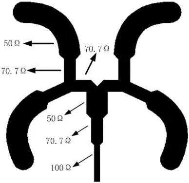
To reduce the loss within the feed network, we introduce the circular-arc feed line to feed each array element. Figure 1 shows the feed network for a 2×2 sub array. In principal, we make the main feed lines orthogonal to each other while ensuring that all the four radiating elements get the same amplitude and phase distribution. Compared to using typical T junctions and bend discontinuities to form a 2×2 element subarray (Examples can be found in [5, 13, 14]), this kind of feed network dramatically improves efficiency due to two facts: 1). Proximity coupling among feed lines causes multiple reflection within the feed network resulting in an increase of loss and a change of excitation currents, while proximity coupling among orthogonal feed lines is relatively weak; 2). T junctions and bend discontinuities generate unwanted radiation at the discontinuity of the feed line which can seriously deteriorate the desired amplitude distribution, while
circular-arc feed lines alleviate the discontinuity. When four 2×2 sub arrays form a 4×4 sub array, main feed lines in the network remain quasi-orthogonal to each other, resulting in a great enhancement of network efficiency.
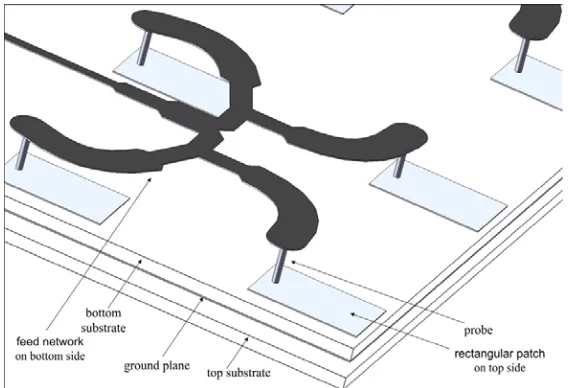
Figure 2. Configuration of the antenna (back view).
In order to reduce the coupling between antenna elements and feed network, we adopt a two-layer structure, as shown in Figure 2. The antenna consists of two Taconic TLT-6 substrates with permittivity 2.65 and thickness 1 mm. Patch elements are pasted on the top side of the top substrate, while the feed network is pasted on the bottom side of the bottom substrate. On the top side of the bottom substrate there is a ground plane, which is designed to separate the two planes and reduce unwanted radiation from various transmission line discontinuities exposed to the radiation plane.
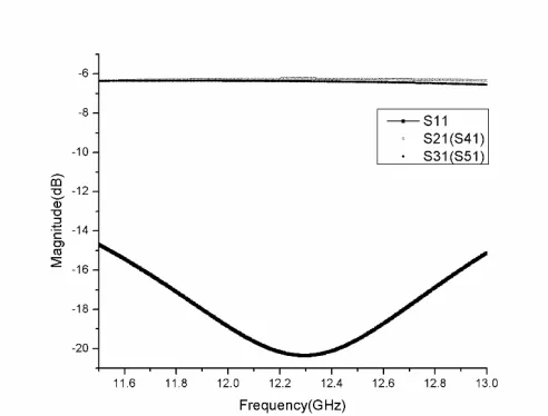
SimulatedS-parameters of the proposed 2×2 feed network using CST Microwave Environment are shown in Figure 3. The simulated
Figure 3. SimulatedS-parameters of the proposed 2×2 feed network.
3. ARRAY CONFIGURATION
The configuration of the proposed antenna array is shown in Figure 2 and photos of fabricated antenna are shown in Figure 4. Simple rectangular patches are used to test the performance of proposed feed network. Rectangular elements (8.65 mm×5 mm) are pasted on the top side of the top substrate. The element spacing of the array is 20.36 mm (or 0.82λ at centre frequency 12.25 GHz). Using reflow soldering technique, probes between the top substrate and bottom substrate connected the rectangular patches and feed network together. A suitable air gap of 1.3 mm thickness is maintained between the two substrates to increase the bandwidth of the antenna due to a decrease in the effective dielectric constant. A ground plane and corporate network is pasted on the top and bottom side of the bottom substrate respectively. The dimensions of the elements and the feed network are optimized to suit a particular requirement of SLL and gain. In short, from the top to the bottom, we have rectangular patch, top substrate, probe, ground plane, bottom substrate and feed network.
4. EXPERIMENTAL RESULTS
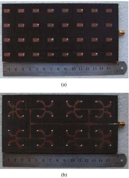
(a)
(b)
Figure 4. Photograph of the fabricated antenna (a) front view (b) back view.
of all, Agilent 8722ES Network Analyzer is used to measure the return loss of the antenna and the result is shown in Figure 5. It can be seen that a good input impedance match characteristics of |S11|<−15 dB over the desired 11.75–12.75 GHz range is obtained.
Figure 6. Measured gain, simulated gain and calculated aperture efficiency of the antenna.
(a) (b)
Figure 7. Measured and simulated normalized radiation pattern (a)
E-plane atf = 12.25 GHz (b) H-plane atf = 12.25 GHz.
of over 22 dBi is obtained, and the aperture efficiency is above 50%. Radiation patterns in E-plane and the pattern in H-plane at centre frequency are measured and plotted in Figure 7, which show the SLL of 13.29 dB in E-plane and 12.3 dB in H-plane, respectively. All experimental results indicate that a high-performance antenna array is obtained by simply using the proposed feed network.
5. CONCLUSION
A novel feed mechanism for high-performance microstrip antenna array is presented. We have used the techniques discussed here to design, develop, manufacture, and measure a 2× 16 array antenna. The complete structure has a 22.93 dBi gain and an aperture efficiency of 70.5% at centre frequency, as well as a stable antenna gain of over 22 dBi and an aperture efficiency of above 50% over the desired 11.75–12.75 GHz range. This feed network also features a stable and reproducible structure, and can be used for microstrip antenna arrays requiring high gain and broadband performance.
ACKNOWLEDGMENT
The work was supported by National Nature Science Fund (60501016). REFERENCES
1. Wang, H., X. B. Huang, D. G. Fang, and G. B. Han, “A microstrip antenna array formed by microstrip line fed tooth-like-slot patches,” IEEE Transactions on Antennas and Propagation, Vol. 55, No. 4, 1210–1214, 2007.
2. Yuan, T., N. Yuan, L.-W. Li, and M.-S. Leong, “Design and analysis of phased antenna array with low sidelobe by fast algorithm,”Progress In Electromagnetics Research, PIER 87, 131– 147, 2008.
3. Abdelaziz, A. A., “Improving the performance of an antenna array by using radar absorbing cover,” Progress In Electromagnetics Research Letters, Vol. 1, 129–138, 2008.
4. Naghshvarian-Jahromi, M., “Novel ku band fan beam reflector back array antenna,” Progress In Electromagnetics Research Letters, Vol. 3, 95–103, 2008.
feed,” IEEE Antennas and Propagation Society International Symposium 2006, 1503–1506, July 9–14, 2006.
6. Horng, T.-S. and N. G. Alexopoulos, “Corporate feed design for microstrip arrays,” IEEE Transactions on Antennas and Propagation, Vol. 41, No. 12, 1615–1624, 1993.
7. Fu, Y. Q., Q. R. Zheng, Q. Gao, and G. H. Zhang, “Mutual coupling reduction between large antenna array using electromagnetic bandgap (EBG) structures,” Journal of Electromagnetic Waves and Applications, Vol. 20, No. 6, 819–825, 2006.
8. He, Q.-Q. and B.-Z. Wang, “Design of microstrip array antenna by using active element pattern technique combining with taylor synthesis method,”Progress In Electromagnetics Research, PIER 80, 63–76, 2008.
9. Splitt, G. and M. Davidovitz, “Guidelines for design of elec-tromagnetically coupled microstrippatch antennas on two-layer substrates,” IEEE Transactions on Antennas and Propagation, Vol. 38, No. 7, 1136–1140, 1990.
10. Jarchi, S., J. Rashed-Mohassel, and M. H. Neshati, “Mutual coupling of rectangular DRA in four element circular array,” Progress In Electromagnetics Resarch Symposium 2007, 2000– 2004, Beijing, China, March 26–30, 2007.
11. Levine, E., G. Malamud, S. Shtrikman, and D. Treves, “A study of microstrip array antennas with the feed network,”IEEE Transactions on Antennas and Propagation, Vol. 37, No. 4, 426– 434, 1989.
12. Lu, K. H. and T.-N. Chan, “Circularly polarized array antenna with corporate-feed network and series-feed elements,” IEEE Transactions on Antennas and Propagation, Vol. 53, No. 10, 3288– 3292, 2005.
13. Gray, D. P., C. B. Ravipati, L. Shafai, “Corporate fed microstrip arrays with non radiating edge fed microstrip patches,” IEEE Antennas and Propagation Society International Symposium 1998, 1130–1133, June 21–26, 1998.