www.ijiset.com
Dual Mode Logic – Design for Energy Efficiency and High
Performance Carry Skip Adder
U. SureshP 1
P
, C. BhargavP 2
P
K. Prasad BabuP 3
P
, K.SudhkarP 4
P
T.ChakrapaniP 5
P
1
P
M.Tech in VLSISD (14G31D5718) ECE, JNTUA Anantapur/SJCET/St.Johns College of Engineering & Technology, Kurnool, A.P 518360, India. [email protected]
P
2
P
ASSISTANT PROFESSOR, ECE, JNTUA Anantapur/SJCET/St.Johns College of Engineering & Technology, Kurnool, A.P 518360, India
P
3,4,5
P
ASSOCIATE PROFESSOR, ECE, JNTUA Anantapur/SJCET/StJohns College of Engineering & Technology, Kurnool, A.P 518360, India
Abstract
The dual mode logic (DML) gates family enables a very high level of energy delay optimization flexibility at the gate level. In this project, this flexibility is utilized to improve energy efficiency and performance of combinatorial circuits by manipulating their critical and noncritical paths. An approach that locates the design's critical paths and operates these paths in the boosted performance mode is proposed. The proposed approach is analyzed on a 16 bit static carry skip adder, DML carry skip adder and Proposed carry skip adder with 102µm X 52 µm. Simulations for 16 bit static carry skip adder, DML carry skip adder and Proposed carry skip adder with 102µm X 52 µm carried out in a standard 45 nm digital CMOS technology and correspondent power, delay are observed.
Keywords: 25TDual Mode Logic, energy efficiency, high
performance, critical paths, energy - delay optimization.
1. Introduction
The first IC flip-flop was built by Jack Kilby in 1958 with 2 transistors at Texas instrument. In 2008, Intel’s Itanium µp contained more than 2 billion transistors and a 16 Gb Flash memory enclosed other than 4 billion transistors. This corresponds to a yearly growth rate of 53% over 50 years. For so long no more technology in record has continued such a high growth rate durable. This absurd growth has come from steady tininess of transistors and improvement in manufacturing processes. Mainly other fields of engineering engage tradeoffs between performance, power, and price. on the other hand, as transistors become smaller, they also dissipate less power, becomes faster, and are cheaper to manufacture. This activity has not solely revolutionized natural philosophy, however conjointly society at giant. Integrated became a $100 billion/year business in 1994. In 2007, the business factory-made roughly half-dozen large integer (6 x billion for each soul on the world. Thousands of engineers have created their fortunes within the field. New fortunes lie
ahead for those with innovative concepts and also the talent to bring those concepts to reality.
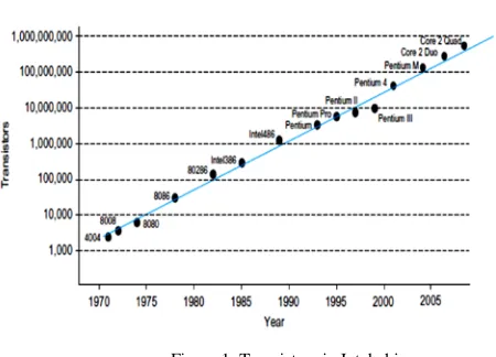
Figure1 shows that the amount of transistors in Intel microprocessors doubled each twenty six months since the invention of the 4004. Moore\'s Law is driven primarily by cutting down the dimensions of transistors and, to a extent, by building larger chips. The extent of integration of chips has been classified as small-scale, medium-scale, large-scale, and extremely giant scale. Small-scale integration (SSI) circuits, like the 7404 electrical converter, have fewer than ten gates, with roughly a dozen transistors per gate
.
Figure 1: Transistors in Intel chip.
www.ijiset.com performance, measured in time to run AN application, has
advanced even quite raw clock speed. Presently, the performance is driven by the amount of cores on a chip instead of by the clock. despite the fact that a personal CMOS electronic transistor uses terribly little energy every time it switches, the big range of transistors shift at terribly high rates of speed have created power consumption a serious design thought once more. Moreover, as transistors became therefore little, the y stop to show fully OFF. Little amounts of current unseaworthy through every electronic transistor currently result in vital power consumption once increased by millions or billions of transistors on a chip. The feature size of a CMOS producing method refers to the minimum dimension of a electronic transistor which will be faithfully designed. The 4004 had a feature size of ten. The Core a pair of pair had a feature size of forty five nm in 2008. Makers introduce a brand new method generation (also referred to as a technology with a half-hour smaller feature size to pack doubly as several transistors within the same space. Figure 1.6 shows the progression of method sizes right down to 0. 25area unit typically per microns (10-6 m), whereas smaller feature sizes area unit expressed in nanometers (10-9) were comparatively minor in metric linear unit processes, like electronic transistor outpouring, variations in characteristics of adjacent transistors, and wire resistance are of nice significance in metric linear unit processes.
2.
INTRODUCTION TO ADDERS
The core of each microprocessor, digital signal processor (DSP), and processing application-specific microcircuit (ASIC) is its knowledge path. it\'s typically the crucial circuit element If power dissipation, die area, and particularly operation speed are of concern it\'s typically the crucial circuit At the center of data-path and addressing units successively are arithmetic units, like comparators, adders, and multipliers. Finally, the basic operation found in most arithmetic parts that the binary addition. Besides of the straightforward addition of 2 numbers, adders are employed in a lot of complex operations like multiplication and division. However additionally less complicated operations like incrementation and magnitude comparison base on binary addition Therefore, binary addition is that the most vital mathematical process. it\'s additionally a awfully crucial one if enforced in hardware as a result of it involves an expensive carry-propagation step, the analysis time of that relies on the quantity word length. The economical implementation of the addition operation in associate microcircuit may be a key downside in VLSI style. Productivity in ASIC style is consistently improved by the utilization of cell based style techniques - like commonplace cells, gate arrays, and field programmable gate arrays (FPGA) - and by low- and high-level synthesis. This asks for adder architectures that end in economical cell-based circuit realizations which may
simply be synthesized. what is more they should offer enough flexibility so as to accommodate custom temporal arrangement and space constraints furthermore on enable the implementation of customized adders.
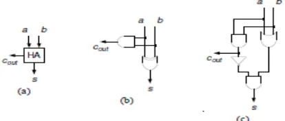
2.1 HALF-ADDER
Half-adder (HA) may be a (2,2)-counter. The a lot of vital add bit is termed carry-out as a result of it carries associate overflow to succeeding higher bit position. Figure2.1 depicts the logic image and 2 circuit implementations of a half-adder. The corresponding, arithmetic and logic equations are given below, at the side of the world and time quality measures below the unit-gate models.
Figure 2.1 :(a) Logic symbol, and (b, c) schematics of a half-adder
Logic equations:
S= a XOR b , Cout= a AND b
2.2 FULL ADDER:
www.ijiset.com
Figure 2.2 :(a) Logic symbol, and (b, c, d, e, f) schematics of a full-adder
Logic Equations : S = a xor b xorcin
Cout= (a and b) or (a and cin) or (b and cin)
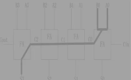
2.3 Ripple-Carry adder
The RCA is constructed via cascading FA blocks in sequence. One FA is accountable for the totaling of 2 binary digits at any phase of the ripple carry. The carry-out of 1 stage is fed directly to the carry-in of the later stage. A no of full adders may be to the RCA or RCA’s of unlike sizes may be cascaded in order to lodge binary vector strings of bigger sizes. N computational elements (FA) are required for an n-bit parallel adder, Figure 4 shows an example of a parallel adder: a 4-bit RCA. It is collected of 4 full adders. The augends bits of x are added to the addend bits of y politely of their binary location. A sum and a carry out are created by each bit 6 addition . The carry-out is then propagated to the carry-in of the next higher-order bit. The resultant output creates a sum of 4 bits + carry out (c4)
.
Figure 2.3(a) Parallel Adder: 4-bit RCA Block Diagram
Although this is easy adder and can be use to add unlimited bit length numbers, it is still not very efficient when big bit No.s are used.
One of the most severe drawbacks of this adder is that the delay and the bit length are increased linearly As mentioned earlier, every full adder has to remain for the carry out of the previous stage to output steady-state result. So still if the adder has a value at its output terminal, it has to wait for the transmission of the carry by the output reach a correct value as shown below fig. Considering over the example in figure 4, the addition of x4 and y4 cannot reach stable state till c4 becomes obtainable In sequence, c4 have to be compelled to watch for c3,
so on all the way down to c1. to finish one operation of a full adder it takes Tfa seconds , in order that the ultimate result can reach its stable-state worth solely after 4Tfa seconds. Its space is n Afa If it\'s illustrious ahead that the primary carry in (c0) can continually be zero then a (very) little area consumption may be achieved (so that the primary full adder may be replaced by a [*fr1] adder). In general, assumptive all gates have constant delay and space of NAND-2 denoted by Tgate and calcedony then this circuit has 3n Tgate delay and 5nAgate. N is that the range of full adders.( In Static CMOS above statement isn\'t true). Gate delays rely on intrinsic delay + fan-in delay +fan-out delay
Figure 2.3(b): Carry Propagation in Carry Ripple Adder
In general the worst case delay of the RCA is once a carry signal transition ripples through all stages of adder chain from significant bit until the foremost vital bit, that is
calculable by
wherever tc determines delay through the carry stage of a full adder, determines delay to calculate the total of the last stage. The delay of RCA is linearly proportional to n ( the quantity of bits) therefore the of the RCA is proscribed once n grows larger. The benefits of the RCA area unit lower power consumption and compact layout providing smaller chip space .Ripple carry adders area unit cascaded to style a bigger adder. Associate example of thirty seven carry propagate adder is given in Fig. 6
www.ijiset.com
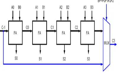
2.4 Carry-Skip Adder A straight forward ripple carry-adder with a special speed up carry chain referred to as a skip chain. This chain describes the distribution of ripple carry blocks, that produce the carry skip adder
Carry Skip Mechanics
The addition of 2 binary digits at stage i, wherever i ?zero, of carry adder depends on the carry in, Ci , that in point of fact is that the perform, Ci-1, of the previous stage. Therefore, so as to calculate the and the perform, Ci+1 , of stage i, it's imperative that the carry in, Ci, be legendary ahead. it's fascinating to notice that in some cases can be calculated while not information of Ci.
These findings would alter U.S.A. to make associate adder whose average time of computation would be proportional to the longest chains of zeros and of different digits of A and B. or else, given 2 binary strings of numbers, like the instance below, it's terribly possible that we have a tendency to could encounter large chains of consecutive bits (block 2) wherever Ai ? metal. so as to handle this state of affairs we have a tendency to should reanalyze equation three rigorously. Equ.five --from Equation one If Ai ? metal ??Ci+1 = Ci --from Equation three within the case of comparison 2 bits of opposite worth,particular stage, can merely be cherish the carry in. thus we are able to merely propagate the carry to consequent stage while not having to attend for the sum to be calculated.
2 Random Bit Strings: A 10100 01011 10100 01011 B 01101 10100 01010 01100
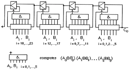
of the last property, we are able to style associate adder that's divided into blocks, as shown in Fig. 7, wherever a special purpose circuit will the two binary strings within every block and confirm if they're equal or not. within the latter case the carry coming into the block can merely be propagated to consequent block and if this can be the case all the carry inputs to the bit positions therein block square measure all either 0's or 1's betting on the carry in into the block. ought to only 1 try of bits (Ai and Bi) within a block be equal then the carry skip mechanism would be unable to skip the block. within the extreme case, though still possible, that there exist one such case, wherever Ai = metal, in every block, then no block is skipped however carry would be generated in every block instead. Carry Skip Chain
In outline the carry skip chain mechanism (Figure2.4) works as follows
Figure 2.4(a): Carry skip chain mechanism
www.ijiset.com
Figure 2.4(b) Carry Bypass Circuit Architecture
The delay of n-bit adder supported m-bit blocks of Carry Bypass Adder, CBA rippled
together are often given by:
n is the adder length and m is the length of the blocks comparison to the RCA, the CBA has slightly improved speed for wider bit adders (still linear to n), however with higher active capacitance and also the space overhead thanks to the additional bypass circuit.
LOW DELAY IN VLSI
In VLSI design, the input signal to an inverter are power and delay which results in static power consumption. The figure of merit during the selection and implementation of a device during chip fabrication. With the improvement in VLSI technology, the transistor count per chip is rapidly growing. Owing to the rise in transistor count, routing complexity of interconnect is increasing, which in turn increasing the length of interconnect. Larger length of interconnect requires more numbers of repeaters .In VLSI chip design, the designing of repeaters thus becomes significant. Less delay, low power consumption and ability to operate at higher frequency ranges are the requirements in the designing of the chip. For the better performance of a chip, the repeater should be able to dissipate less power and less delay it should also be able to operate at higher frequencies. Ismail and Friedman proposed RLC line method [4] in repeater insertion process showed that on-chip inductance could decrease the area, delay and power of the repeater insertion process as compared to an RC line model. Increased length of interconnects are obtained by increasing the complexity of interconnects. The long interconnections lead to high propagation delays. To drive high capacitive loads, Buffers are required so as to keep pace with the required speed. Hence number of buffers are required to be inserted at regular intervals of distance in interconnect for the proper detection and reconstruction of the signal, which are termed as repeaters .Single buffer is not sufficient. Numerous optimization efforts have been made [6-8] for medium performance and medium power consumption designs. Illustrious methods include switching activity
reduction, voltage scaling and logic optimization .Though, these methods are not sufficient in many applications where ultra-low power consumption with medium frequency of operation is the primary concerns, such as portable computing gadgets, medical electronics etc., The system must have a miniaturized power supply in order to achieve portability . So a portable system must be designed for low power consumption. Supply voltage scaling is an effective way to reduce power consumption. For low power applications, sub-threshold operation is a better option. However, threshold voltage cannot be scaled down with the same rate. Because of trade-off between power and speed, low power systems are slower ones. At medium frequencies the repeater circuit operating in sub-threshold region is the best option. The sub-sub-threshold logic operates with the threshold voltage Vt of the transistor is greater than power supply VDD. In this paper the sub threshold grounded-body biasing technique is proposed, having both PMOS and NMOS bodies grounded and
calculation and simulation ensure the enhanced
performance than the conventional repeater. Here ability to operate at higher frequencies without compromising with the power dissipation in sub-threshold region and emphasis is on the lower delay. The STGB style of the repeater works at higher frequencies having lower delay,
which in turn reduces power-delay product.
3. INTRODUCTION TO DUAL MODE
LOGIC:
Now a day’s rapidly growing mobile communications and day to day in grow thing in electronic industry applications power consumption is become a problem in VLSI digital design. And recently sub-threshold circuit in digital design these method of design mostly prepared in ultra-low power applications.
One thing we should know that they utilize a supply voltage or VDD is less than the threshold voltage of the transistors when circuits are operating in the sub-threshold region due to this reduction of both dynamic power and static power. However supply voltage at each scaling which results degrades the performance and much sensitivity should be high to process of variations and temperature fluctuations.
www.ijiset.com operates in feature in dynamic mode achieve much higher
performance but with increased the power dissipation. The dual mode logic (DML) provides in unique feature to control the system performance applications in which a workload should be required in flexible.
DML gates should operate at very low voltages i.e. 300mV it is possible to making a high immunity to process variations. if NAND or NOR gates should performs simulations indicate while operating in the dynamic mode , sub threshold Dual Mode Logic or DML can achieve an improvement in speed of up to 10x compared to standard complementary metal oxide semiconductor or CMOS ,while dissipating more power dissipation. In static mode a 5x reduction of power should be achieved compared to previous logic which these expense of magnitude decrement in performance. Monte carlo simulations of Dual Mode Logic or DML present a significant improvement in robustness as compared to dynamic logic or domino logic.
EXISTING SYSTEM:
Dynamic logic, such as domino logic, has been used since the 1970’s for high-performance applications. In the past, there have been several attempts to use dynamic logic in sub threshold to improve the speed. However, these attempts did not gain momentum because of high sensitivity to process variations in nano technologies.
Figure 3.1: Existing system
• Dynamic logic or Domino logic is used for high performance.
• Not suitable for high speed operation.
• Not suitable for complex mixed signal
amplification on SoC technology.
• Transistors in the circuits are operated based on saturation region. It will increase the supply voltage.
• In this circuit power consumption is low compare to normal NAND gate. Further power consumption is reduced by connecting a NMOS
footer switch. The combination of PMOS header switch and NMOS footer switch.
In this paper we proposed Dual Mode Logic (DML) should be designed to operate in sub-threshold region. This proposed logic can be operated in two different modes. They are given below i.e.
Static mode
Dynamic mode
The above two modes circuits can be implemented with complementary metal oxide semiconductor (CMOS) devices. In static we use static CMOS and in dynamic mode we use dynamic np-CMOS.
In static mode the DML gates has very low power dissipation. But in this mode performance should be in moderate. Static mode is also called as DC mode. In static mode the power dissipation mainly occurred due to supply voltage.
In dynamic mode the DML gates has higher performance but it leads higher power dissipation. Dynamic mode is also called as AC mode. Because in this mode power dissipation increased due to given input signal. This input signal is in the form of AC.
PROPOSED SYSTEM:
Dual mode logic (DML), designed to activate in the sub threshold state. In two modes the proposed logic can be operated: static CMOS-like mode and dynamic
np-CMOS-like mode
Figure 3.2: proposed system
Power gating controllers can controls the power provided by the CMOS switches. Outputs of the power gated block gets discharge slowly. Thus voltage levels of output should be spend more time in threshold voltage level. Due to this short circuit current should be increased.
www.ijiset.com • If we insert the sleep transistors can transfers the chip
power network into a permanent power network to the power supply or VDD and Virtual Power network that drives the cells and gets turned off the circuit.
• During active mode, sleep transistors are on, then reduced resistance increases current while reducing delay
• During sleep mode, sleep transistors are off, stacked transistors suppress leakage current while saving state • We can apply high threshold voltage (high-Vth), which is not used in the forced stack technique due to the dramatic delay increase.
DML circuits should be shows the high immunity to process variations and also it should be operate in very low voltage i.e. in terms of 300mV.
We should perform the NAND or NOR gates Simulations which indicate that sub-threshold DML should achieves the improvement in speed has high compared to standard CMOS similarly it dissipating mode power while operating in dynamic mode. But in static mode half percentage of power dissipation should be reduced when compared to the power dissipation of dynamic mode. It has less performance.
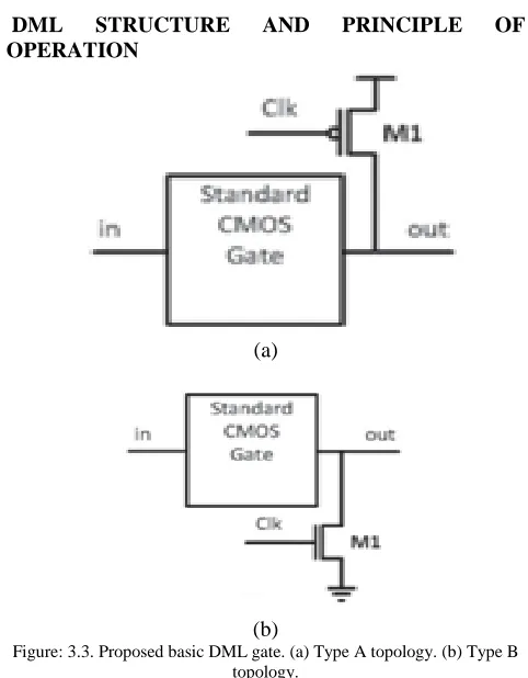
DML STRUCTURE AND PRINCIPLE OF OPERATION
(a)
(b)
Figure: 3.3. Proposed basic DML gate. (a) Type A topology. (b) Type B topology.
The basic DML gate architecture was composed of a standard CMOS gate and an additional transistor M1, it has a gate, drain and source terminal, in which gate
should be connected to global clock shown in above figure.
At first glance, this architecture is very similar to the noise tolerant pre charge (NTP) structure, introduced by Yamada et al... But the noise tolerant pre-charge (NTP) was developed in the high speed, high noise tolerant in dynamic logic. Here dual mode logic or DML can allow the operation in two modes that is static mode or DC mode and Dynamic mode or AC mode.
In the dynamic mode the input signal is given to the gate terminal that input is called as a asymmetric clock, which allowing two different phases i.e. pre-charge and evaluation. During the pre charge phase, the output should be charged to high level or low level depending on the topology of the gate terminal of the DML structure.
In the above evaluation phase, the output should be evaluated according to the values given at the gate inputs. The proposed system of DML topologies marked as a Type A and Type B should be illustrated in above shown figure.
Type B has an added n-MOS transistor that pre charges the output to a logical “0” during the precharge phase. Type A has an added p-MOS that pre charges the output to a logical “1.” Dynamic logic gates should be implemented by using high threshold voltage such as footer, which requires additional transistor. Here the high Vt footer should be used to decrease pre charge time by eliminating the data through the different nodes and allowing faster pre charge.
Changing the DML gate to operate in static mode operation is fairly the global Clk should be fixed high for Type A topology and constantly should be low for Type B topology. In which as a result, the gate attains a similar topology to CMOS, except the negligible parasitic capacitance.
DML node can be create based on a CMOS gate is also very simple: “gluing” an additional transistor for the pre charge phase, and, in the case of a footed gate, an adding a additional transistor such as a footer in type A topology and a p-MOS transistor as a header in Type B gates.
When designing a DML gate should be replace the pre-charge transistor in parallel to the stacked transistors when design methodology should be used. Hence the evaluation and analysis should be performed with the parallel transistors due to this we should say this is faster circuit.
www.ijiset.com during the evaluation and during static operation to
decrease leakage currents. All gates should be designed either a Type A or Type B based on the based on the ignoring the optimization guidelines these are mentioned the above. Even though this design methodology will allow maximum performance, minimize area, and maximize power efficiency, it is possible to connect gates of the same type by using an buffering inverter between them, it is done in domino logic. when a footer or header should be used in each stage by Connecting gates of the same type without any inverter circuits, however, this structure will cause glitching after should be ending the pre charge and data flowing through the chain until the evaluation completed.
However standard dynamic logic, inherent keeper of DML logic helps recover the logical value.
RESULTS:
STATIC CMOS FULL ADDER CIRCUIT :
OUTPUT WAVE FORM
MUX IN DML
OUTPUT WAVE FORM
www.ijiset.com
16 BIT CARRY SKIP ADDER
OUTPUT WAVEFORM
16 BIT CARRYSKIP IN DML
OUTPUT WAVEFORM
PROPOSED CARRY SKIP ADDER IN DML
www.ijiset.com
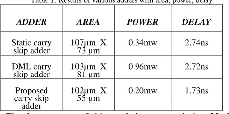
4. Conclusions
Comparative analysis of various types of carry skip
adders :
Table 1: Results of various adders with area, power, delay
0B
ADDER 1BAREA 2BPOWER 3BDELAY
Static carry
skip adder 107µm X 73 µm 0.34mw 2.74ns DML carry
skip adder 103µm X 81 µm 0.96mw 2.72ns Proposed
carry skip adder
102µm X
55 µm 0.20mw 1.73ns
The future scope of this work is we can design 32- bit carry skip adder and 64- bit carry skip adders by using the Dual Mode logic, with area power and delay considerations.
References
[1] Chandrakasan, R. Brodersen, ―Low Power Design‖, Kluwer Academic Publishers, 1995.
[2] A. M. Shams, and M. A. Bayoumi, ―A Novel High Performance CMOS 1-Bit Full Adder Cell‖, IEEE Transactions on Circuit and System, vol.47, NO. 5,May, 2000.
[3] J. H. Kang and J. B. Kim, ―Design of a Low Power CVSL Full Adder Using Low-Swing Technique‖, ICSE2004 Proc. 2004, Kuala Lumpur, Malaysia.