Recursive Approach to the Design of a Parallel Self-Timed
Adder
*Naveen & ** D. Koteshwar Rao
*
M-Tech Student Ganapathy Engineering College, Rangasaipet, Hunter Road, Warangal **Associate Professor ECE Dept Ganapathy Engineering College, Rangasaipet, Hunter Road, WarangalAbstract
—
This brief presents a parallel single-rail self-timed adder. It is based on a recursive formulation for performing multibit binary addition. The operation is parallel for those bits that do not need any carry chain propagation. Thus, the design attains logarithmic performance over random operand conditions without any special speedup circuitry or look-ahead schema. A practical implementation is provided along with a completion detection unit. The implementation s regular and does not have any practical limitations of high fanouts. A high fan-in gate is required though but this is unavoidable for asynchronous logic and is managed by connecting the transistors in parallel. Simulations have been performed using an industry standard toolkit that verify the practicality and superiority of the proposed approach over existing asynchronous adders.
I. INTRODUCTION
Binary addition is the single most important operation that a processor performs. Most of the adders have been designed for synchronous circuits even though there is a strong interest in clockless/ asynchronous processors/circuits [1]. Asynchronous circuits do not assume any quantization of time. Therefore, they hold great potential for logic design as they are free from several problems of clocked (synchronous) circuits. In principle, logic flow in asynchronous circuits is controlled by a request- acknowledgment handshaking protocol to establish a pipeline in the absence of clocks. Explicit handshaking blocks for small elements, such as bit adders, are expensive. Therefore, it is implicitly and efficiently managed using dual-rail carry propagation in adders. A valid dual-rail carry output also provides acknowledgment from a single-bit adder block. Thus, asynchronous adders are either based on full dual-rail encoding
constitute a single-rail cyclic asynchronous sequential adder [4]. Cyclic circuits can be more resource efficient than their acyclic counterparts [5], [6]. On the other hand, wave pipelining (or maximal rate pipelining) is a technique that can apply pipelined inputs before the outputs are stabilized [7]. The proposed circuit manages automatic single-rail pipelining of the carry inputs separated by propagation and inertial delays of the gates in the circuit path. Thus, it is effectively a singlerail wave-pipelined approach and quite different from conventional pipelined adders using dual-rail encoding to implicitly represent the pipelining of carry signals.
The remainder of this brief is organized as follows. Section II provides a review of self-timed adders. Section III presents the architecture and theory behind the proposed adder. Sections IV and V provide CMOS implementation and simulation results for the proposed adder. Section VI draws the conclusion.
II. BACKGROUND
There are a myriad designs of binary adders nd we focus here on asynchronous self-timed adders. Self-timed refers to logic circuits that depend on and/or engineer timing assumptions for the correct operation. Self-timed adders have the potential to run faster averaged for dynamic data, as early completion sensing can avoid the need for the worst case bundled delay mechanism of synchronous circuits. They can be further classified as follows.
A. Pipelined Adders Using Single-Rail Data Encoding
The asynchronous Req/Ack handshake can be used to enable the adder block as well as to establish the flow of carry signals. In most of the cases, a dual-rail carry convention is used for
internal bitwise flow of carry outputs. These dual-rail signals can represent more thantwo logic values (invalid, 0, 1), and therefore can be used to generate bit-level acknowledgment when a bit operation is completed. Finalcompletion is sensed when all bit Ack signals are received (high). The carry-completion sensing adder is an example of a pipelined adder [8], which uses full adder (FA) functional blocks adapted for dual-rail carry. On the other hand, a speculative completion adder is proposed in [9]. It uses so-called abort logic and early completion to select the proper completion response from a number of fixed delaylines. However, the abort logic implementation is expensive due to high fan-in requirements.
B. Delay Insensitive Adders Using Dual- Rail Encoding
A further optimization is provided from the observation that dualrail encoding logic can benefit from settling of either the 0 or 1 path. Dual-rail logic need not wait for both paths to be evaluated. Thus, it is possible to further speed up the carry look-ahead circuitry to send carry-generate/carry-kill signals to any level in the tree. This is elaborated in [8] and referred as DICLA with speedup circuitry (DICLASP).
III. DESIGN OF PASTA
In this section, the architecture and theory behind PASTA is presented. The adder first accepts two input operands to perform halfadditions for each bit. Subsequently, it iterates using earlier generated carry and sums to perform half-additions repeatedly until all carry bits are consumed and settled at zero level.
A. Architecture of PASTA
The general architecture of the adder is shown in Fig. 1. Theselection input for two-input multiplexers corresponds to the Req handshake signal and will be a single 0 to 1 transition denoted by SEL. It will initially
select the actual operands during SEL = 0 and will switch to feedback/carry paths for subsequent iterations usingSEL = 1. The feedback path from the HAs enables the multiple iterations to continue until the completion when all carry signals willassume zero values.
B. State Diagrams
In Fig. 2, two state diagrams are drawn for the initial phase and the iterative phase of the proposed architecture. Each state is represented by (Ci+1 Si) pair where Ci+1, Si represent carry out and sum values, respectively, from the ith bit adder block. During the initial phase, the circuit merely works as a combinational HA operating in fundamentalmode. It is apparent that due to the use of HAs instead of FAs, state (11) cannot appear.
During the iterative phase (SEL = 1), the feedback path throughmultiplexer block is activated. The carry transitions (Ci ) are allowed as many times as needed to complete the recursion.
From the definition of fundamental mode circuits, the present design cannot be considered as a fundamental mode circuit as theinput–outputs will go through several transitions before producing the final output. It is not a Muller circuit working outside the fundamentalmode either as internally, several transitions will take place, as shown in the state diagram. This is analogous to cyclic sequential circuits where gate delays are utilized to separate individual states [4].
B. Recursive Formula for Binary Addition
Let S j i and C j i+1 denote the sum and
iteration. The initial condition ( j = 0) for
addition is formulated as follows:
Now, the correctness of the recursive formulation is inductively proved as follows.
Theorem 1: The recursive formulation of (1)–(4) will produce correct sum for any number of bits and will terminate within a finite time.
Proof: We prove the correctness of the algorithm by induction on the required number of iterations for completing the addition (meetingthe terminating condition).
Basis: Consider the operand choices for which no carry propagation is required, i.e., C0 i= 0 for ∀i, i ∈ [0..n]. The proposed formulation will produce the correct result by a single-bit computation time and terminate instantly as (4) is met
.Induction: Assume that Ck i+1_= 0 for some ith bit at kth iteration. Let l be such a bit for which
Ckl+1= 1. We show that it will be successfully transmitted to next higher bit in the (k + 1)th iteration. As shown in the state diagram, the kth iteration of lth bit state(Ckl+1, Sk l ) and (l + 1)th bit state (Ckl+2, Skl+1) could be in anyof (0, 0), (0, 1), or (1, 0) states. As Ckl+1= 1, it implies thatSkl = 0. Hence, from (3), Ck+1 l+1= 0 for any input condition between0 to l bits.
We now consider the (l + 1)th bit state (Ckl+2, Skl+1) for kth iteration. It could also be in any of
(0, 0), (0, 1), or (1, 0) states. In (k+1)th iteration, the (0, 0) and (1, 0) states from the kth iteration will correctly produce output of (0, 1) following (2) and (3). For(0, 1) state, the carry successfully propagates through this bit level following (3). Thus, all the single-bit adders will successfully kill or propagatethe carries until all carries are zero fulfilling the terminating condition.
The mathematical form presented above is valid under the condition that the iterations progress synchronously for all bit levels and the required input and outputs for a specific iteration will also bein synchrony with the progress of one iteration. In the next section, we present an implementation of the proposed architecture which is subsequently verified using simulations.
IV. IMPLEMENTATION
is negated to obtain an active high completion signal (TERM). This requires a large fan-in n -input NOR gate. Therefore, an alternative more practical pseudo-nMOS ratio-ed design is used. The resulting design is shown in Fig. 3(d). Using the pseudo-nMOS design, the completion unit avoids the high fan-in problem as all the connections are parallel. The pMOS transistor connected to VDD of this ratio-ed design acts as a load register, resulting in static current drain when some of the nMOS transistors are on simultaneously. In addition to the Ci s, the negative of SEL signal is also included for the TERM signal to ensure that the completion cannot be accidentally turned on during the initial selection phase of the actual inputs. It also prevents the p MOS pull up transistor from being always on. Hence, static current will only be flowing for the duration of the actual computation. VLSI layout has also been performed [Fig. 3(e)] for a standard cell environment using two metal layers. The layout
occupies 270 λ × 130 λ for 1-bit resulting in
1.123 Mλ2 area for 32-bit. Thepull down
transistors of the completion detection logic are included in the single-bit layout (the T terminal) while the pull-up transistor is additionally placed for the full 32-bit adder. It is nearly double the area required for RCA and is a little less than the most of the area efficient prefix tree adder, i.e., Brent–Kung adder (BKA). V. SIMULATION RESULTS In this section, we present simulation results for different adders
using Mentor Graphics Eldo SPICE version 7.4_1.1, running on 64-bit Linux platform. For implementation of other adders, we have used standard library implementations of the basic gates. The custom adders such as DIRCA/DICLASP are implemented based on their most efficient designs from [8]. Initially, we show how the present design of PASTA can effectively
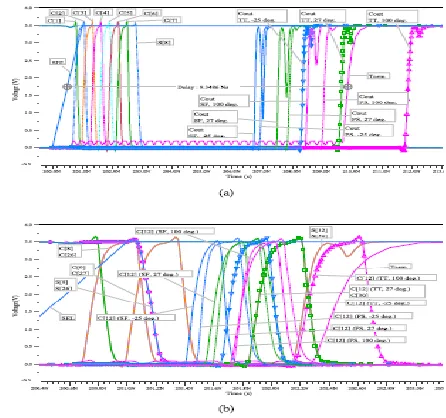
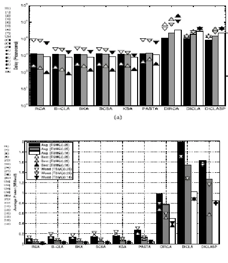
propagates through successive bit adders like a pulse as evident from Fig. 4(a). The best-case corresponding to minimum length carry chain (not shown here) does not involve any carry propagation, and hence incurs only a single-bit adder delay before producing the TERM signal. The worst-case involves maximum carry propagation cascaded delay due to the carry chain length of full 32 bit. The independence of carry chains is evident from the average case [Fig. 4(b)] where C8 and C26 are shown to trigger at nearly the same time. This circuit works correctly for all process corners. For SF corner cases, one Cout rising edge in Fig. 4(a) shows a short dynamic hazard. This has no follow on effects in the circuit nor are errors induced by the SF extreme corner case. The delay performances of different adders are shown in Fig. 5. We have used 1000 uniformly distributed random operands to represent the average case while best case, worst case correspond to specific test-cases representing zero, 32-bit carry propagation chains respectively. The delay for combinational adders is measured at 70% transition point for the result bit that experiences the maximum delay. For self-timed adders, it is measured by the delay between SEL and TERM signals, as depicted in Fig. 4(a). The 32-bit full CLA is not practical due to the requirement of high fan-in, and therefore a hierarchical block CLA (B-CLA), as shown in [8], is implemented for comparison. The combinational adders, such as RCA/B-CLA/BKA/ Kogge–Stone adder (KSA)/Sklansky’s conditional sum adder (SCSA) can only work for the worst-case delay as they do not have any completion sensing mechanism. Therefore, these results give an empirical upper bound of the performance enhancement that can be achieved using these
adders as the basic unit and employing some kind of completion sensing technique.
Fig. 4. SPICE timing diagram for PASTA implementation using TSMC 0.35 μm process. The Cout and C12 for worst case and average case, respectively, are shown for different conditions where TT, SF, and FS represents typical–typical, slow-fast, and fast–slow nMOS– pMOS conditions in these figures. (a) Worst-case carry propagation while adding operands (FFFF
that, PASTA completes the first iteration of the recursive formulation when ―SEL = 0.‖
Therefore, the best case delay represents the delay required to generate the TERM signal only and of the order of picoseconds. Similar overhead is also present in dual-rail logic circuits where they have to be reset to the invalid state prior to any computation. The dynamic/nMOS only designs require a precharge phase to be completed during this interval. These overheads are not included in this comparison. The best case and worst case carry performances of DIRCA for the chosen operands are nearly the same, as one rail needs to be set from start to end. In contrast, the average cases can have carry generation and killing in any bit and thus providing a better case for DIRCA. However, even the average case results for dual-rail adders cannot beat the worst-case performance by RCA. This is in contrast
Fig. 5. (a) SPICE timing report for different 32-bit adders. (b) Comparison of average power consumptions by different 32-bit adders. RCA: Ripple carry adder. KSA: Kogge–Stone adder. B-CLA: block carry look-ahead adder. PASTA: parallel self-timed adder. BKA: Brent–Kung adder. DIRCA: delay insensitive RCA. SCSA: Sklansky’s conditional sum adder. DICLASP: delay insensitive carry look-ahead adder with special circuitry.
The results presented in [8], and we identify a few reasons for this anomaly as follows.
1) The original CMOS implementation by [8] uses MOSIS 2 μm, level two CMOS parameters while our implementation uses submicrometer and deep submicrometer SPICE level 3, Eldo SPICE level 53 CMOS (corresponding to Berkeley
BSIM V3.3)parameters.
2) All DI designs under evaluation are based on data driven dynamic logic circuits. The performance of these dynamic circuits can be optimized using larger nMOS transistors in the pull-down network. However, it will considerably increase precharge delay as the load capacitance will also increase for pMOS transistors. Therefore, we have kept the standard sizing of nMOS and pMOS transistors that will result in equal rise/fall time in this circuit.
3) The original results were obtained without consideration of factors such as layout, wiring delays, stray capacitance, and noise [8].
5) The data driven dynamic logic cannot attain the same performance as the pure dynamic logic circuits since they often include more than one pull-up pMOS transistor which increases the switching delay.
Another interesting observation is that the performances of the combinational adders and PASTA improve with the decreasing process width and VDD values while the performance of dual-rail adders decreases with scaling down of the technology. This results from the fact that dynamic logic requires technology specific energy delay optimization as performed in [12]. We also note that the dynamic logic switching speed advantage can be attributed to the nMOS threshold voltage being lower than a static CMOS threshold voltage (VDD/2), which diminishes with decreasing process width. The PASTA layout complies with all design rules for the TSMC 0.35 μm process and this was found to increase the delay by two to three times after taking into consideration layout specific parasitic capacitances. Similar performance degradation is expected for other adders when layout effects are considered. The average power consumption of different adders for different operand choices (best, worst, and average carry chain lengths) are shown in Fig. 5. We measure average power consumed by combinational and self-timed adders for the duration of input pattern placement and completion of the addition. Combinational static CMOS circuits show significantly lower power consumption than self-timed DI adders. PASTA consumes a little more average power than combinational adders as it uses a transmission gate based XOR implementation which consumes more average power. RCA is the most efficient adder as it consumes the least amount of verage power. Among DI adders DIRCA is the best and
consumes nearly 3.6, 6.2, and 11.38 times the average power of PASTA for SMC 0.35, 0.25, and 0.18 μm processes, respectively. All adders show decreasing average power consumption as the process length is decreased and PASTA consumes least power among the self-time dadders.
VI. CONCLUSION
This brief presents an efficient implementation of a PASTA. Initially, the theoretical foundation for a single-rail wave-pipelinedadder is established. Subsequently, the architectural design and CMOS implementations are presented. The design achieves a very simple n-bit adder that is area and interconnection-wise equivalent to the simplest adder namely the RCA. Moreover, the circuit works in a parallel manner for independent carry chains, and thus achieves logarithmic average time performance over random input values. The completion detection unit for the proposed adder is also practical and efficient. Simulation results are used to verify the advantages of the proposed approach.
REFERENCES
[1] D. Geer, ―Is it time for clockless chips? [Asynchronous processor chips],‖ IEEE Comput., vol. 38, no. 3, pp. 18–19, Mar. 2005.
[2] J. Sparsø and S. Furber, Principles of Asynchronous Circuit Design. Boston, MA, USA: Kluwer Academic, 2001.
[4] M. Z. Rahman and L. Kleeman, ―A delay matched approach for the design of asynchronous sequential circuits,‖ Dept. Comput. Syst.Technol., Univ. Malaya, Kuala Lumpur, Malaysia, Tech. Rep. 05042013, 2013.
5] M. D. Riedel, ―Cyclic combinational circuits,‖ Ph.D. dissertation, Dept. Comput. Sci., California Inst. Technol., Pasadena, CA, USA, May 2004.
[6] R. F. Tinder, Asynchronous Sequential Machine Design and Analysis:A Comprehensive Development of the Design and Analysis of Clock-Independent State Machines and Systems. San Mateo, CA, USA: Morgan, 2009.
Authors profile : - NAVEEN completed his b tech and pursuing m tech in ganapathi engineering college