International Journal of Research (IJR)
e-ISSN: 2348-6848, p- ISSN: 2348-795X Volume 2, Issue 10, October 2015Available at http://internationaljournalofresearch.org
Design and Implementation of Efficient Reversible Vedic
multiplier for Low Power and High Speed Operations
1
C.Himam Hussain
PG Scholar, Sri Krishnadevaraya Engineering College, Gooty, Andhra Pradesh, India
2
B. Balasubbanna
Associate Prof,Sri Krishnadevaraya Engineering College, Gooty, Andhra Pradesh, India
Abstract:
Multipliers are vital components of any processor or computing machine. More often than not,
performance of microcontrollers and Digital signal processors are evaluated on the basis of number of
multiplications performed in unit time. Hence better multiplier architectures are bound to increase the
efficiency of the system. Vedic multiplier is one such promising solution. It’s simple architecture coupled
with increased speed forms an unparalleled combination for serving any complex multiplication
computations. Tagged with these highlights, implementing this with reversible logic further reduces
power dissipation. Power dissipation is another important constraint in an embedded system which
cannot be neglected. In this paper we bring out a Vedic multiplier known as “Urdhva Tiryakbhayam”
meaning vertical and crosswise, implemented using reversible logic, which is the first of its kind. This
multiplier may find applications in Fast Fourier Transforms (FFTs), and other applications of DSP like
imaging, software defined radios, wireless communications.
For exiting system we are using 4-bit
multiplier,but the given proposed system we are implementing 8-bit multiplier using reversible vedic
mathematics approach as shown in above diagram.
Keywords :
reversible gates ; Urdhva Tiryakbhayam; DSP; vedic multiplier
1. INTRODUCTION:
Multiplication is of immense importance in Digital Signal Processing (DSP) and Image Processing (IP). To implement the hardware module of Discrete Fourier Transformation (DFT), Discrete Cosine Transformation (DCT), Discrete Sine Transformation (DST) and modem broadband communications; large numbers of complex multipliers are required. Complex number multiplication is performed using four real
number multiplications and two additions/
subtractions.In real number processing, carry needs to be propagated from the least significant bit (LSB) to the most significant bit (MSB) when binary partial products are added. Therefore, the addition and subtraction after binary multiplications limit the overall speed. Many alternative method had so far been proposed for complex number multiplication like algebraic transformation based implementation, bit-serial multiplication using offset binary and distributed arithmetic, the CORDIC (coordinate rotation digital
computer) algorithm, the quadratic residue number system (QRNS), and recently, the redundant complex number system (RCNS) .Blahut et. al proposed a technique for complex number multiplication, where the algebraic transformation was used. This algebraic transformation saves one real multiplication, at the expense of three additions as compared to the direct method implementation. A left to right array for the fast multiplication has been reported in 2005, and the method is not further extended for complex multiplication. But, all the above techniques require either large overhead for pre/post processing or long latency. Further many design issues like as speed, accuracy, design overhead, power consumption etc., should not be addressed for fast multiplication.
International Journal of Research (IJR)
e-ISSN: 2348-6848, p- ISSN: 2348-795X Volume 2, Issue 10, October 2015Available at http://internationaljournalofresearch.org
carrypropagation for rapid additions and subtractions. Mehta et al. have been proposed a multiplier design using "Urdhva-tiryakbyham" sutras, which was adopted from the Vedas. The formulation using this sutra is similar to the modem array multiplication, which also indicating the carry propagation issues. Multiplier implementation in the gate level (FPGA) using Vedic Mathematics has already been reported but to the best of our knowledge till date there is no report on transistor level (ASIC) implementation of such complex multiplier.
The multiplier is fully parameterized, so any configuration of input and output word-lengths could be elaborated. Transistor level implementation for performance parameters such as propagation delay, dynamic leakage power and dynamic switching power consumption calculation of the proposed method was calculated by spice spectra using 90 nm standard CMOS technology and compared with the other design like distributed arithmetic parallel adder based implementation and algebraic transformation based implementation. The calculated results revealed (16, 16) x (16,16) complex multiplier have propagation delay only 4ns with 6.5 mW dynamic switching power.
2.EXISTING METHOD:
Booth's
multiplication
algorithm
is
a
multiplication algorithm that multiplies two
signed binary numbers in two's complement
notation. The algorithm was invented by Andrew
Donald Booth in 1950 while doing research on
crystallography. A binary multiplier is an
electronic circuit used in digital electronics, such
as a computer, to multiply two binary numbers. It
is built using binary adders. A variety of computer
arithmetic techniques can be used to implement a
digital multiplier. Most techniques involve
computing a set of partial products, and then
summing the partial products together. This
process is similar to the method taught to primary
schoolchildren for conducting long multiplication
on base-10 integers, but has been modified here
for application to a base-2 (binary) numeral
system
ALGORITHM
•
Booth's algorithm examines adjacent pairs
of bits of the N-bit multiplier Y in signed two's
complement representation, including an implicit
bit below the least significant bit, yi-1 = 0. For
each bit yi, for i running from 0 to N-1, the bits yi
and yi-1 are considered.
•
Where these two bits are equal, the
product accumulator P should be right shifted.
Where yi = 0 and yi-1 should the multiplicand is
added to P and then right shifted and where yi = 1
and yi-1 = 0, the multiplicand is subtracted from P
and then right shifted. The final value of P is the
signed product. High speed arithmetic operations
are very important in many signal processing
applications. Speed of the digital signal processor
(DSP) is largely determined by the speed of its
multipliers. In fact the multipliers are the most
important part of all digital signal processors; they
are very important in realizing many important
functions such as fast Fourier transforms and
convolutions.
Since
a
processor
spends
considerable amount of time in performing
multiplication, an improvement in multiplication
speed can greatly improve system performance.
Multiplication can be implemented using many
algorithms such as array, booth, carry save,and
wallace tree algorithm.The computational time
required by the array ¬multiplier is less because
the partial products are computed -independently
in parallel. The delay associated with the array
multiplier is the time taken by the signals to
propagate through the gates that form the
multiplication array .
International Journal of Research (IJR)
e-ISSN: 2348-6848, p- ISSN: 2348-795X Volume 2, Issue 10, October 2015Available at http://internationaljournalofresearch.org
3.1REVERSIBLE LOGIC GATES:
Reversible computing was started when the basis of thermodynamics of information processing was shown that conventional irreversible circuits unavoidably generate heat because of losses of information during the computation. The different physical phenomena can be exploited to construct reversible circuits avoiding the energy losses. One of the most attractive architecture requirements is to build energy lossless small and fast quantum computers. Most of the gates used in digital design are not reversible for example NAND, OR and EXOR gates. A Reversible circuit/gate can generate unique output vector from each input vector, and vice versa, i.e., there is a one to one correspondence between the input and output vectors. Thus, the number of outputs in a reversible gate or circuit has the same as the number of inputs, and commonly used traditional NOT gate is the only reversible gate. Each Reversible gate has a cost associated with it called Quantum cost. The Quantum cost of a Reversible gate is the number of 2*2 Reversible gates or Quantum logic gates required in designing. One of the most important features of a Reversible gate is its garbage output i.e., every input of the gate which is not used as input to other gate or as a primary output is called garbage output. In digital design energy loss is considered as an important performance parameter. Part of the energy dissipation is related to non-ideality of switches and materials. Higher levels of integration and new fabrication processes have dramatically reduced the heat loss over the last decades. The power dissipation in a circuit can be reduced by the use of Reversible logic.
Reversible Function:The multiple output Boolean functionF(x1; x2; :::; xn) ofnBoolean variables is called reversible if:The number of outputs is equal to the number of inputs; Any output pattern has a unique pre-image. In other words, reversible functions are those that perform permutations of the set of input vectors.
3.2 MATHEMATICAL FORMULATION OF VEDIC SUTRAS:
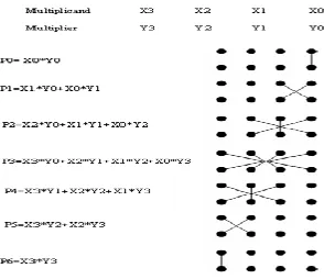
The gifts of the ancient Indian mathematics in the world history of mathematical science are not well recognized. The contributions of saint and mathematician in the field of number theory, 'Sri BharatiKrsnaThirthaji Maharaja', in the form of Vedic Sutras (formulas) are significant for calculations. He had explored the mathematical potentials from Vedic primers and showed that the mathematical operations can be carried out mentally to produce fast answers using the Sutras. In this paper we are concentrating on "Urdhva-tiryakbyham",. A. "Urdhva-tiryakbyham " Sutra The meaning of this sutra is "Vertically and crosswise" and it is applicable to all the multiplication operations.
Fig 3.1: Multiplication procedure using "Urdhva-tiryakbyham " sutra.
3.3
IMPLEMENTATION
OF
VEDIC
MULTIPLIER IN REVERSIBLE LOGIC:
The multiple output Boolean function F (x1 , x2 , ..., xn) of n Boolean variables is called reversible if
The number of outputs is equal to the
number of inputs;
Maps each input assignment to unique
output assignment and vice versa.
International Journal of Research (IJR)
e-ISSN: 2348-6848, p- ISSN: 2348-795X Volume 2, Issue 10, October 2015Available at http://internationaljournalofresearch.org
3.2 Important Parameters in Reversible Logic Circuit Designing:
Number of constant inputs (Gin):
The inputs that are added to an n*k function to make it reversible are called constant inputs.
Number of garbage outputs (Gout):
Garbage outputs are some outputs that are not used for further computations in the circuit.
Number of Gates (NOG):
The number of reversible gates used to realize the function.
Quantum Cost (QC):
The Quantum Cost (QC) of a reversible circuit is defined as the number of 1*1 or 2*2 reversible quantum or logic gates that are needed to realize the circuit.
Total logical calculations (circuit cost): One of the main factors of a circuit is its hardware complexity.
α = A two input EX-OR gate calculation.
β = A two input AND gate calculation .
δ = A NOT calculation.
T = Total logical calculation.
3.6Circuit Optimization:
3.5 REVERSIBLE CIRCUIT:
Fig 3.3.2.2*2 Multiplier.
2-bit multiplier is realized using partial products (earlier 2-bit multiplier is realized using k-map Boolean equations).
To reduce garbage output and constant inputs, tools gate is used in 2-bit multiplier circuit. Half adder gates (peres gates) and 2-cnot gate(xor gate) is used in circuit where no carry is generated in the circuit and Hence full adder gate can be replaced with them.
Fig.3.4. optimization of 4-bit full adder.
International Journal of Research (IJR)
e-ISSN: 2348-6848, p- ISSN: 2348-795X Volume 2, Issue 10, October 2015Available at http://internationaljournalofresearch.org
subtractors units were established. In this work, we present a new design of the reversible half subtractor based on the quantum gates implementation of the reversible TR gate.The reversible TR gate is designed from 2x2 quantum gates such as CNOT and Controlled-V and Controlled-V + gates.
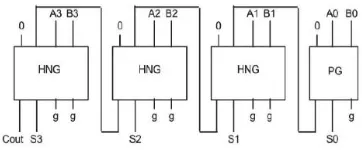
Fig:3.5 Architecture of 8*8 UT Multiplier.
3.6 APPLICATIONS OF REVERSIBLE LOGIC:
Reversible computing may have applications in computer security and transaction processing, but the main long term benefit will be felt very well in those areas which require high energy efficiency, speed and performance it include the area like
Low power CMOS.
Quantum computer.
Nanotechnology.
Optical computing.
DNA computing.
Computer graphics.
Communication.
Design of low power arithmetic
and data path for digital signal
processing (DSP).
Field Programmable Gate Arrays
(FPGAs) in CMOS technology.
Nano computing.
Bio Molecular Computation.
Laptop/Handheld/Wearable.
Computers Spacecraft.
4.RTL SCHEMATICS AND RESULT
4.1 RTL FOR REVERSIBLE VEDIC MULTIPLIER FOR 8 BIT:
4.2 INTERNAL SCHEMATIC FOR REVERSIBLE VEDIC MULTIPLIER FOR 8 BIT:
International Journal of Research (IJR)
e-ISSN: 2348-6848, p- ISSN: 2348-795X Volume 2, Issue 10, October 2015Available at http://internationaljournalofresearch.org
4.4 SIMULATION RESULT:
4.5 DEVICE UTILIZATION SUMMARY
FOR REVERSABLE VEDIC MUTIPLIER:
4.6 COMPARISON TABLES:
Comparison table for Booth multiplier specification of device xc3s500e-4fg320
Comparison table for reversible vedic multiplier specification of device xc3s500e-4fg320
The above table’s shows a comparison between the paper based technique and reversible vedic multiplier based technique in terms of delay in nsec , memory used ,number of lut’s used for the design, and power in mw for 256 bits.
CONCLUSION:
The focus of this paper is mainly to design a low power high speed multiplier which is done by constructing the multiplier using reversible logic gates. The procedure is arried ut so as to yield an optimized design as compared to those in the literature. The efficiency of a reversible logic circuit is characterized in terms of parameters such as quantum cost, number of constant inputs, garbage outputs and number o gates utilized to realize the logic implementations. Lower the value of these parameters more efficient is the design. In parameter called TRLIC had been proposed which is defined as sum of all cost metrics of the given design. The quantum cost is a parameter that directly reflects the delay of the quantum circuit. Also lower TRLIC implicitly means lower the quantuam cost, hence lower is the delay vice versa. Besides imbibing the design criterion that fan-out must be generated within the circuit, he proposed designs also reduce the TRLIC as compared to the previously proposed design. The further optimization of the circuit in terms of the total logical costs is under progress and is taken as future work.
5. REFERENCES:
[1] R. Landauer, “Irreversibility and Heat Generation in the Computational Process”, IBM Journal of Research Development, 5,1961, 183-191.
International Journal of Research (IJR)
e-ISSN: 2348-6848, p- ISSN: 2348-795X Volume 2, Issue 10, October 2015Available at http://internationaljournalofresearch.org
[3] M. Haghparast, M. Mohammadi, K. Navi, and M. Eshghi, 2009, Optimized Reversible Multiplier Circuit, Journal of Circuits, Systems and Computer
Sciences, 18(2):311-323, DOI:
10.1142/S0218126609005083, 2009.
[4] M. Perkowski, A. Al-Rabadi, P. Kerntopf, A. Buller, M. Chrzanowska-Jeske, A. Mishchenko, M. Azad Khan, A. Coppola, S. Yanushkevich, V. Shmerko and L. Jozwiak, A general decomposition for reversible logic, Proc. RM’2001, Starkville, (2001) pp. 119-138.
[5] M. Mohammadi, M. Haghparast, M. Eshghi, and K. Navi, 2009. Minimization and Optimization of Reversible BCD-Full Adder/Subtractor Using Genetic Algorithm and Don’t Care Concept. International Journal of Quantum Information Processing, 7 (5): 969-989, DOI: 10.1142/S0219749909005523.
[6] MajidHaghparast and K. Navi, Novel Reversible Fault Tolerant Error Coding and Detection Circuits, International Journal of Quantum Information, 2011, 9(2): 723-738.
[7] D. Maslov, G. W. Dueck, D. M. Miller: Toffoli Network Synthesis With Templates, IEEE TCAD of Integrated Circuits and Systems, 24, 06, (2005), 807-817.
[8] M. Haghparast, K. Navi, 2007: A Novel Reversible Full Adder Circuit for Nanotechnology Based Systems, J. Applied Sci., 7(24), 3995-4000.
[9] M. Haghparast, K. Navi, 2008. A Novel reversible BCD adder for nanotechnology based systems, Am. J. Applied Sci., 5(3): 282-288.
[10] MD. Saiful Islam and Zerina Begum, Reversible Logic Synthesis Of Fault Tolerant Carry Skip BCD Adder, Journal of Bangladesh Academy of Sciences, Vol. 32, No. 2, 193-200, 2008
[11] SomayehBabazadeh and MajidHaghparast,
Design of a Nanometric Fault Tolerant Reversible
Multiplier Circuit, Journal of Basic and Applied Scientific Research, 2012, 2(2):1355-1361.
[12] R. Feynman, “Quantum Mechanical Computers,” Optics News, Vol. 11, pp. 11–20, 1985.
[13] T. Toffoli, “Reversible Computing,” Tech memo MIT/LCS/TM-151, MIT Lab for Comp.Sci, 1980.
[14] A. Peres, Reversible logic and quantum computers, Physical Review: A, 32 (6) (1985) 3266-3276.
[15] M. Haghparast, K. Navi, 2008: A Novel Fault Tolerant Reversible Gate For Nanotechnology Based Systems, Am. J. Applied Sci., 5(5), 519-523. World Appl. Sci. J., 3(1): 114-118.
[16] M. Haghparast, K. Navi, 2008. Design of a Novel
Fault Tolerant Reversible Full Adder For
Nanotechnology Based Systems.
[17] E. Fredkin and T. Toffoli, “Conservative logic,” Int’l J. Theoretical Physics, Vol. 21, pp.219–253, 1982.
[18] B. Parhami, “Fault Tolerant Reversible Circuits” Proc. 40th Asilomar Conf. Signals, Systems, and Computers, Pacific Grove, CA, Oct. 2006.
[19] P.Saravanan, P. Chandrasekar, LivyaChandran,
NikillaSriram, and P. Kalpana, Design and