IJEDR1601017
International Journal of Engineering Development and Research (www.ijedr.org)103
Performance Enhancement of DC to DC Boost
Converter Based on PID Controller using Automatic
Tuning Method
1
Abhishake Dutta,
2Baljit Singh
1
M-Tech student
, 2Assistant Professor
Department Of Electrical Engineering, Daviet, Jalandhar, India
________________________________________________________________________________________________________
Abstract - This research paper confer the improvement of operating characteristics of DC-DC Boost converter applying PID controller. Primarily we studied the Dc-Dc converter. After that we obtained the state space model of the Dc-Dc converter and using this state space model a transfer function is derived. Next we design the converter in Matlab/Simulation environment. Later we obtain the output response of the designed boost converter. Then we incorporate a PID controller tuned manually in conjunction with designed converter and output results are again obtained. Now we used the obtained transfer function with the PID controller in a unity feedback closed loop model for auto-tuning to get the output response. At the end all the three output results obtained are compared and conclusion is drawn. All simulations have been carried out in Matlab/Simulink environment.
IndexTerms – DC- DC Boost Converter, State Space Average Model,Transfer function of Boost Converter, PID Controller ________________________________________________________________________________________________________
I.INTRODUCTION
With the advancement in technology of the power semiconductor devices and integrated circuit, the applications of power electronics become wider. The task of a power converter is to control and process the flow of electric energy by supplying currents and voltages in a form that are accepted optimally by the various loads. Early electromechanical converters (mostly rotating machines) are used for this purpose[1]. Today, with the development and the mass production of power semiconductors, static power converters find applications in numerous domains and especially in particle accelerators. They have better static and dynamic performances and they are smaller and lighter as compared to their electromechanical counterparts. Every convertor posses its significant importance as per the application and the requirement in the related field.[2]
II. DC TO DC CONVERTERS
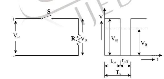
DC- to- DC converter supplies a regulated DC output voltage through a variable-load from a fluctuating DC input voltage. Usually, the input DC voltage that is obtained by rectifying a line voltage gets changed in magnitude. The switching action is generally required in dc-to-dc converters to control the DC output voltage, as shown by the basic DC-DC converter shown in Fig 1 (a).
Vin
+
-S
R Vin
V0
ton toff
Ts
V
t V0
Figure 1: (a) Basic DC – DC converter. (b) DC- DC converter voltage waveforms.
During past two decades, DC-DC converters with silicon-controlled rectifiers (SCRs) were in use as the switching mechanisms and are known as choppers [1]. Now-a-days, DC-DC converters employ insulated gate bipolar transistors (IGBTs) and metal oxide silicon field effect transistors (MOSFETs) and are classified as switch mode power supplies (SMPS). The regulated average output voltage in a DC-DC converter depends on the pulse width, on-time of the switch, and the switching frequency Fs [3].
III. BOOST CONVERTERS
IJEDR1601017
International Journal of Engineering Development and Research (www.ijedr.org)104
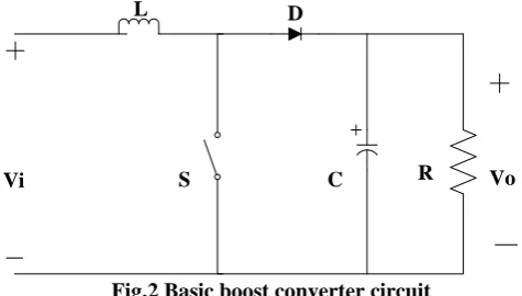
providing energy from the inductor and the source to increase the average output voltage. The boost converter is commonly used in regulated DC power supplies and regenerative braking of DC motors. The circuit that models the basic operation of the boost converter is shown in Fig 2 The boost converter uses the same components as the buck converter with different placement. The input voltage in series with the inductor acts as a current source. The energy stored in the inductor builds up when the switch is closed. When the switch is opened, current continues to flow through the inductor to the load. Since the source and the discharging inductor are both providing energy with the switch open, the effect is to boost the voltage across the load. The load consists of a resistor in parallel with a filter capacitor. The capacitor voltage is larger than the input voltage. The capacitor is large to keep a constant output voltage and acts to reduce the ripple in the output voltage [9].L D
S C
Vi R Vo
Fig.2 Basic boost converter circuit
IV. GENERAL BOOST CONVERTER CONFIGURATION
Fig 3 shows the basic blocks of building a boost converter circuit. The voltage source provides the input DC voltage to the switch control, and also to the magnetic field storage element. The block which contains switch control directs the action of the switching element, whereas the output rectifier and filter deliver an acceptable DC voltage to the output [15] .
Voltage source
Switch Control
Switch Element
Output Rectifier and Filter Circuit Magnetic
Field Storage Elemment
Figure 3 Block diagram of Boost Converter Circuit
The DC-DC Switching Boost Converter is designed to provide an efficient method of taking a given DC voltage supply and boosting it to a desired value. Power for the boost converter can come from any suitable DC sources, such as DC generators, batteries, solar panels and rectifiers. A boost converter using a power MOSFET is shown below in figure 4.
VC
S1 C R Vo
S2 L
Vg
Figure 4 Boost Converter Circuit using MOSFET as switching element
The function of boost converter can be divided into two modes, Mode 1 and Mode 2. Mode 1 begins when switch S1 is switched on during time dTs. The current from the source flows in the inductance L and switch S1. The value of current increases linearly
with time in this interval, with (dIg/dt) being positive. As the current through L increases, the polarity of the induced emf is taken
as say, positive, the left hand side of L being +ve [2]. The equation for the circuit is,
𝑉𝑔
=
L 𝑑𝐼𝑔𝑑𝑡
Or
𝑑𝐼𝑔 𝑑𝑡 =
𝑉𝑔
𝐿
Mode 2 begins when transistor S1 is switched off and S2 is switched on during time (1- d)Ts. As the current through L decreases, with its direction being in the same direction as shown (same as in the earlier case), the induced emf reverses, the left hand side of L being -ve. So, the induced emf (taken as –ve in the equation given later) is added with the supply voltage, being of the same polarity, thus, keeping the current (Ig = Io) in the same direction. The energy stored in inductor L flows through the load. The
current (Ig = Io) decreases linearly in the time interval, as the output voltage is assumed to be nearly constant at vo = VO with
IJEDR1601017
International Journal of Engineering Development and Research (www.ijedr.org)105
VO= Vg
+
L dIgdt Or
dIg dt =
(Vo− Vg)
L
V. STATE SPACE AVERAGE MODEL
Figure 5 describes the circuit for mode I of operation of boost converter. The mode I is during time dTs when the switch S1 is on
and switch S2 is OFF. The state space matrices for the operation mode I of the given boost converter model is as under
[𝑖𝑙
.
𝑣𝑐.] = [
0 0
0 −1 𝑅𝐶⁄ ] [ 𝑖𝐿
𝑣𝐶] + [ 1 𝐿
0] [𝑣
𝑔] And 𝑣𝑜 = [0 1][
𝑖𝐿
𝑣𝐶]
L
S1 C Vo
Vg Vc R
iL
Figure 5 Circuit for mode I of Operation
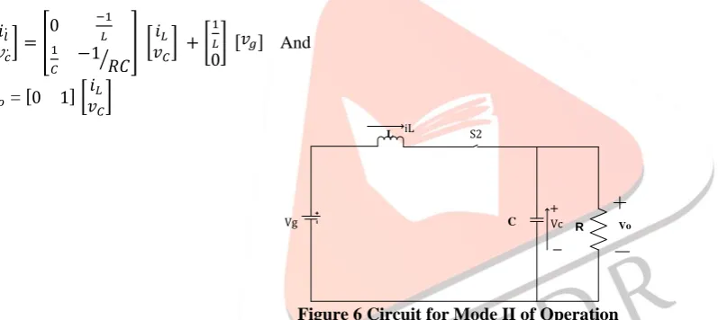
Figure 6 describes the circuit for mode II of operation of boost converter. The mode II is during time (1- d) Tswhen the switch S1
is OFF and switch S2 is ON. The state space matrices for the operation mode I of the given boost converter model is as under
[𝑖𝑙
.
𝑣𝑐.] = [
0 −1
𝐿 1 𝐶
−1 𝑅𝐶 ⁄ ] [
𝑖𝐿
𝑣𝐶] + [ 1 𝐿
0] [𝑣
𝑔] And
𝑣𝑜 = [0 1][
𝑖𝐿
𝑣𝐶]
L S2
C Vo
Vg Vc R
iL
Figure 6 Circuit for Mode II of Operation
The average large signal model for the complete boost converter circuit can be obtained by adding the two state space matrices obtained during two modes of operation i.e. mode I and II using the equation A = A1d + A2(1-d) . The average large signal of the
given boost circuit is given as under
[𝑖𝑙.
𝑣𝑐.] = [
0 −(1−𝑑)
𝐿 (1−𝑑)
𝐶
−1 𝑅𝐶 ⁄ ] [
𝑖𝐿
𝑣𝐶] + [ 1 𝐿
0] [𝑣
𝑔]
And
𝑣𝑜 = [0 1][
𝑖𝐿
𝑣𝐶]
Average large signal model comprises of two parts i.e. steady state part and small signal part as under
[𝐼𝐿 + 𝑖̂𝑙
.
𝑉𝐶+ 𝑣̂𝑐.] = [
0 −(1−𝐷−𝑑̂)
𝐿 (1−𝐷−𝑑)̂
𝐶
−1 𝑅𝐶 ⁄
] [𝐼𝐿+ 𝑖̂𝐿 𝑉𝐶+ 𝑣̂𝐶] + [
1 𝐿
0] [𝑉𝑔 + 𝑣̂𝑔]
And
𝑣𝑜 = [0 1][
𝐼𝐿+ 𝑖̂𝐿
𝑉𝑐+ 𝑣̂𝐶]
The steady state part of the average large signal model represented by the upper case letters IL, like VC, Vg and D are all set to zero
IJEDR1601017
International Journal of Engineering Development and Research (www.ijedr.org)106
[𝑖̂𝑙
.
𝑣̂𝑐.] = [
0 −(1−𝐷)
𝐿 (1−𝐷)
𝐶
−1 𝑅𝐶 ⁄ ] [
𝑖̂𝐿
𝑣̂𝐶] + [
0 𝑑̂
𝐿 −𝑑̂
𝐶 0
] [𝐼𝑉𝐿
𝑐] + [ 1 𝐿
0] [𝑣̂𝑔]
Or
[𝑖̂𝑙
.
𝑣̂𝑐.] = [
0 −(1−𝐷)
𝐿 (1−𝐷)
𝐶 −1⁄𝑅𝐶
] [𝑖̂𝐿 𝑣̂𝐶] + [
𝑉𝐶 𝐿 −𝐼𝐿
𝐶
] [𝑑̂] + [
1 𝐿
0] [𝑣̂𝑔]
Output equations
𝑣̂𝑜 = [0 1] [
𝑖̂𝑙
𝑣̂𝑐
]
The steady state output and input voltage relationship can derived from the given equation
VO = - [0 1][
0 −(1−𝐷)
𝐿 (1−𝐷)
𝐶 −1⁄𝑅𝐶
] [
1 𝐿
0][Vg] 𝑉𝑂
𝑉𝑔
= 1 1 − 𝐷
VI. TRANSFER FUNCTION IN S-DOMAIN
The requisite relationship between the output voltage and the control input d (duty cycle) for designing the necessary controller is given as under
𝑽𝒐 𝒅(𝒔)=
−𝟐𝟎𝟎(𝒔−𝟐𝒆𝟎𝟎𝟓) 𝒔𝟐 +𝟐.𝟎𝟖𝟑𝒔+𝟒.𝟏𝟔𝟕𝒆𝟎𝟎𝟓
The derived transfer relationship between output voltage Vo and controlled input d is used in unity feedback closed loop system in conjunction with PID controller so as to get the desired results.
VII. PID CONTROLLER
A proportional-integral-derivative controller (PID controller) is a feedback control loop mechanism i.e. Widely used in many industrial applications. A PID controller calculates an error value i.e. the difference between a desired set point and the actual value measured. The controller attempts to minimize this error by manipulating the variables through the process known as tuning [4].
The PID controller algorithm involve three different steady parameters, and for that reason occasionally called three-term control: the proportional, the integral and derivative values, denoted P,I, and D. Figure 7 shows the basic block diagram of a PID controller. Where P depends on the current error, I on the gathering of precedent errors, and D is a forecast of upcoming errors, based on present rate of transform. The biased sum of these three events is used to regulate the procedure by means of a control element such as a damper, the position of a control valve or the power delivered to a heating element.
A number of applications may call for using only one or two actions to offer the suitable system control. This can be achieved by setting the other parameters to zero. A PID controller will be called a P, I, PI or PD controller in the absence of the respective control actions [5]
.
Figure 7Block diagram of PID controller
VIII. PID TUNING
Tuning a control loop is the amendment of its control parameters (proportional gain, integral gain, derivative gain) to the best possible values for the most wanted control response. Steadiness (no unbounded oscillation) is a fundamental requirement, but
1 𝑠
𝑑𝑣 𝑑𝑡 𝐾𝑑
𝐾𝑖 𝐾𝑝
IJEDR1601017
International Journal of Engineering Development and Research (www.ijedr.org)107
ahead of that, different systems have different performance, different applications have different necessities, and necessities may clash with one another [4].PID tuning is a not an easy problem, although there are only three parameters because it must convince complex criteria within the restrictions of PID control. There are accordingly various methods for loop tuning, and classier techniques are the subject of patents; this section describes some regular manual methods for loop tuning [7].
Designing and tuning a PID controller appears to be theoretically intuitive, but can be hard in practice and often conflicting, if several objectives such as high stability and short transient are to be achieved. PID controllers regularly provide satisfactory control using default tunings, but performance can usually be enhanced by careful tuning, and performance may be disagreeable with poor tuning. Generally, preliminary designs must be adjusted continually through computer simulations until the closed-loop system performs as desired [5].
IX. MANUAL TUNING
With the system left online, one tuning method is to initially setting all parameters to nil. Raise until the output of the loop oscillates, and after that should be set to just about half of that value for a "quarter amplitude decline" type comeback. At that moment enhance until any offset is corrected in satisfactory time for the process. Yet, too much increase will cause unsteadiness. Lastly, increase, if essential, until the loop is well enough quick to arrive at its position after a load annoyance. On the other hand, in excess of will cause unnecessary response and overshoots. A quick PID loop tuning generally go beyond a little to arrive at the set position more rapidly; still, some systems cannot agree to overshoots, in such a case an over-damped closed-loop system is requisite, which will call for a setting considerably less than half of setting that was resulting in oscillations [26].
Table 1: Effect of Independent P, I and D Tuning Closedloop
Response
Rise Time Overshoot Settling time Steady state Error Stability Increasing KP
Decrease Increase Small Increase
Decrease Degrade
Increasing KI
Small Decrease
Increase Increase Large Decrease Degrade Increasing KD Small Decrease
Decrease Decrease Minor Change
Improve
X. AUTOMATIC PID TUNING
MATLAB provides tools without human intervention for choosing best possible PID gains which makes the hit and trial method described over an unnecessary one. We are able to access the tuning algorithm straightforwardly using PID tune or through a nice graphical user interface (GUI) using PID tool. The MATLAB programmed tuning algorithm chooses PID gains to get robustness (stability margins) and balance the performance (bandwidth, response time). By default the algorithm designed for sixty degrees phase margin.
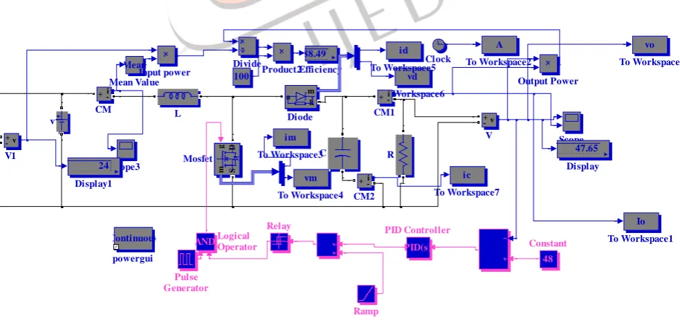
XI. SIMULINK MODEL FOR BOOST CONVERTER
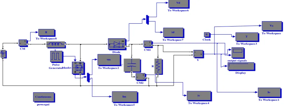
Given below is a circuit diagram used for MATLAB simulation of boost converter. The purpose of this circuit is to measure output voltage and current waveform. The DC-DC Switching Boost Converter will take a 24 Volt DC voltage supply and deliver 47.65 Volts to the load. The maximum current delivered to the load will be 0.2A. The inductor shown in Fig acts as the magnetic field storage element. It stores energy in its core material. The power stage has two inputs: the input voltage and the duty cycle. The duty cycle is the control input, i.e., this input is a logic signal which controls the switching action of the switching element, i.e. mosfet and hence the output voltage. The frequency of operation is 100 kHz. Duty Cycle is maintained at 50 %
Figure 8 Showing the Simulink model of Boost converter without PID controller [15]
IJEDR1601017
International Journal of Engineering Development and Research (www.ijedr.org)108
Figure 9 Showing Output voltage (VO) without any controllerTable 2: Output of Boost converter without any controller
Sr. No.
Parameter Values1
Rise Time .00245 seconds2
Settling Time 0.3468 sec3
Peak Value 78.5 Volts4
Overshoot 64.75 %5
Settled voltage 47.65 VoltsXII. SIMULINK MODEL FOR BOOST CONVERTER USING PID CONTROLLER
In order to get acceptable performance, the PID controller that contains all the control components (proportional, derivative, and integral) is used in the given model of boost converter. The constants KP, KD and KI can be adjusted to get the desired output with minimum overshoot voltage and less settling time. This adjustment process is called tuning the controller. In the given work, auto tuning method is used. For this, I found the overall transfer function of the given model. Then I used the derived transfer function with the PID controller in closed loop model for auto tuning to get the values of KP, KI and KD.
Figure 10 Showing the Simulation Diagram of Boost converter with PID controller
0 0.2 0.4 0.6 0.8 1 1.2 1.4 1.6 1.8 2
0 10 20 30 40 50 60 70 80 Time (Seconds) A mp li tu d
e ( O
IJEDR1601017
International Journal of Engineering Development and Research (www.ijedr.org)109
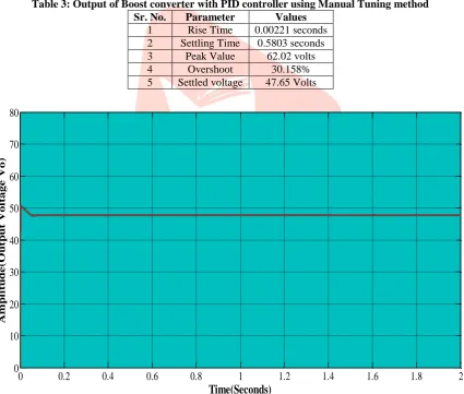
Figure 11 Showing Output voltage (VO) with manually tuned PID controllerTable 3: Output of Boost converter with PID controller using Manual Tuning method Sr. No. Parameter Values
1 Rise Time 0.00221 seconds 2 Settling Time 0.5803 seconds 3 Peak Value 62.02 volts
4 Overshoot 30.158%
5 Settled voltage 47.65 Volts
Figure 12 Showing Output voltage (VO) with automatically tuned PID controller
Table 4: Output of Boost converter using automatic tuning method of PID controller
0 0.2 0.4 0.6 0.8 1 1.2 1.4 1.6 1.8 2
0 10 20 30 40 50 60 70 80
Time(Seconds)
A
mp
li
tu
d
e
(O
u
tp
u
t V
ol
tage
V
o)
0 0.2 0.4 0.6 0.8 1 1.2 1.4 1.6 1.8 2
0 10 20 30 40 50 60 70 80
Time(Seconds)
A
mp
li
tu
d
e
(O
u
tp
u
t V
ol
tage
V
o)
Sr. No. Parameter Values 1 Rise Time 0.0019 seconds 2 Settling Time 0.08281 sec 3 Peak Value 50.78 Volts
4 Overshoot 6.57 %
IJEDR1601017
International Journal of Engineering Development and Research (www.ijedr.org)110
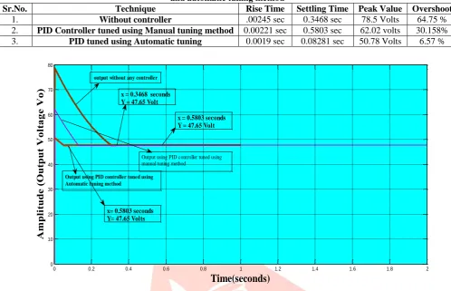
Table 5: Comparison of output results for Boost Converter without any Controller, PID controller tuned using Manualand automatic tuning method
Sr.No. Technique Rise Time Settling Time Peak Value Overshoot 1. Without controller .00245 sec 0.3468 sec 78.5 Volts 64.75 % 2. PID Controller tuned using Manual tuning method 0.00221 sec 0.5803 sec 62.02 volts 30.158% 3. PID tuned using Automatic tuning 0.0019 sec 0.08281 sec 50.78 Volts 6.57 %
Figure 13 showing the comparison between Output voltage in three cases
As the previous table shows the compression of different techniques on the bases of parameters Rise time, Settling time, Peak value and Overshoot. With the help of table we can conclude that Automatic tuning Technique gives best results as compare to without any controller and Manual tuning method.
Table 6: Table showing the general system parameters of Boost Converter used in this work
Sr.No. Parameters Values 1 Input Voltage (Vg) 24 Volts
2 Input Current (Ig) 0.4 ma
3 Capacitance ( C ) 2000µF
4 Inductance ( L ) 300µH
5 Switching Frequency ( F ) 100KHz 6 Load Resistance ( R ) 240 Ω
7 Duty Ratio (D ) 0.5
XIII. CONCLUSION
This work discusses the performance of DC to DC Boost converter without any controller, conventional tuning and the Automatic tuning PID controller method. Two methods have been described in detail that is automatic tuning and conventional tuning method for PID tuning.
Dc-Dc Converters are widely used for traction motor in electric automobiles, trolley cars, marine hoists, and forklift trucks. They provide smooth acceleration control, high efficiency, and fast dynamic response. General idea of dc-dc converter is to convert a fixed voltage dc source into a variable voltage dc source. In the beginning of 1970s, a good number of DC-DC converter circuits have been designed and analyzed in detail. Such converter circuits can amplify or reduce the scale of the DC voltage and/or reverse its polarity. In the topology known as Boost converter, the inductor is used in series with input voltage source, which allows this converter to produce an output DC voltage that is greater in magnitude than the input voltage.
A proposed model for DC to DC Boost converter with and without any controller is constructed in MATLAB/SIMULINK. Output results for Boost converter with and without controller are obtained. From the results obtained above can be concluded that the Automatic Tuning method to tune PID controller gives much better in overall performance in terms of rise time, peak overshoot and settling time as compared to manual tuning method and without controller.
XIV. FUTURE SCOPE: By looking at the number of papers published in recent year and work done in these thesis following scope is for future:
0 0.2 0.4 0.6 0.8 1 1.2 1.4 1.6 1.8 2
0 10 20 30 40 50 60 70 80
Time(seconds)
A
m
pl
itud
e
(Outp
ut
V
o
lta
g
e
V
o
)
output without any controller
Output using PID controller tuned using Automatic tuning method
x = 0.3468 seconds Y = 47.65 Volt
Output using PID controller tuned using manual tuning method
x = 0.5803 seconds Y = 47.65 Volt
IJEDR1601017
International Journal of Engineering Development and Research (www.ijedr.org)111
1. Next step of this study is to implement this Boost converter simulink model in real time environment using variouscomponents and PID Controller and get the desired results.
2. To optimize the performance of given Boost Converter model using various optimization techniques like genetic algorithm, PSO and comparing the results with this study.
3.
To design the Boost converter model, for maintaining constant voltage at the output irrespective of the variable voltage at the input side and for varying loads.
XV.ACKNOWLEDGMENT
The authors are thankful to the management DAVIET Engineering College Jalandhar, Punjab for providing all the computational facilities to carry out this work successfully.
REFERENCES
[1] Ashfaq Ahmed. Power Electronics For Technology, pp. 1-427, Prentice Hall, 1998. [2] B.R.Gupta, V. Singhal. Power Electronics pp 1- 600, S.K. Kataria & Sons, 2009.
[3] M.H.Rashid Power electronics Circuits, Devices and Applications,pp.1-912 Prentice Hall, 2003.
[4] J. C. Basilio and S. R. Matos, “Design of PI and PID Controllers With Transient Performance Specification” IEEE Transactions On Education, VOL. 45, NO. 4, November 2002, pp. 364-370,2002
[5] Kiam Heong Ang, Gregory Chong and Yun Li, Member , “PID Control System Analysis, Design and Technology”, IEEE Transactions On Control Systems Technology, VOL. 13, NO. 4, July 2005, pp. 559-576,2005.
[6] Sreekumar C, Vivek Agarwal, “Hybrid Control of a Boost Converter Operating in Discontinuous Current Mode” Power Elecronics Specialists Confrence, 2006 PESC, pp. 1-6,2006.
[7] Xinping Ding, Zhaoming Qian, Shuitao Yang, Bin Cuil, Fangzheng Peng, “A PID Control Strategy for DC Link Boost Voltage in Z – Source Inverter,” Applied Power Electronics Conference, Apec Twenty Second Annual IEEE, pp. 1145 – 1148,2007.
[8] H. El Fadil and F. Giri, “Robust and Nonlinear Control of PWM DC-to-DC Boost Power Converters,” pp.407-412, IEEE 2007.
[9] A. Khaligh, A. M. Rahimi, A. Emadi, “Modified Pulse Adjustment Technique to Control Dc/Dc Converters Driving Variable Constant Power Loads,” IEEE Transactions on Industrial Electronics Vol. 55 No. 3, pp. 1133 -1146,IEEE 2008..
[10] Mariko Shirazi, Regan Zane, Dragan Maksimovic, “An Auto tuning Digital Controller for DC-DC Power Converters Based on Online Frequency Measurement,” IEEE Transactions on Power Electronics Vol. 24, No. 11, pp. 2578-2588, 2009.
[11] R. Firat Tigrek, “Simple Efficiency Formula for Regulated DC-to-DC Converters,” IEEE Transactions on Aerospace and Electronic Systems Vol. 46, No. 4, pp. 2123-2130, 2010.
[12] Gabriel Ortiz, Dominik Bortis, Johann W. Kolar, Jürgen Biela, “Optimal Design of a 3.5 KV/11KW DC – DC Converters for Charging Capacitor Banks for Power Modulators,” IEEE Transactions on Plasma Science, Vol. 38, No. 10, pp. 2565-2573, 2010. [13] S. N. Deepa, G. Sugumaran , “Design of PID Controller for Higher Order Continuous Systems using MPSO based Model Formulation Technique”, International Scholarly and Scientific Research & Innovation, Vol:5, August 2011, pp. 1004- 1010,2011.
[14] Mitul kumar R. Dave K.C. Dave, “Analysis of Boost Converter Using PI Control Algorithms,” International Journal of Engineering Trends and Technology, Vol. 1, No. 2, pp. 71-73, 2012.
[15] Sumita Dhali, P. Nageshwara Rao, Praveen Mande, “PWM-Based Sliding Mode Controller for DC-DC Boost Converter,” International Journal of Engineering Research and Applications, Vol. 2, No. 1, pp. 618 - 623, 2012.
[16] Arjyadhara Pradhan, Dr S.M Ali, Chitrlekha Jena and Puspapriya Behera, “Design and Simulation of DC-DC Converter Used in Solar Charge Controllers”, International Journal of Engineering Inventions, Volume 2, Issue 3, February 2013 PP: 59-62,2013.
[17] S. Sendil Kumar, V. Devaraj, R. Ravi Kumar, P. Hem Kumar, V. Megala, G. Merlin Subha and S. Amudhapriya, “ Implementation of Direct AC-DC Boost Converter for Low Voltage Energy Harvesting,” International Journal of Engineering Science Innovation, Vol. 2, No. 3, pp. 08 - 16, 2013.
[18] Barry W. Williams, “DC-to-DC Converters with Continuous Input and Output Power,” ,” IEEE Transactions on Power Electronics Vol. 28, No. 5, pp. 2307-2316, 2013.
[19] Thanana Nuchkrua and Thananchai Leephakpreeda, “Adaptive PID Control of DC-link Voltage via DC/DC Buck Boost converter,” Thammasat International Journal of Engineering Science Innovation, Vol. 18, No. 2, pp. 42 - 53, 2013.
[20] Alberto Rodriguez, Marcos Fernandez, Aitor Vazquez, Diego. G. Lamar, Manuel Arias and Javier Sebastian, “Optimizing the Efficiency of a DC-DC Boost Converter Over 98% by Using Commercial SiC Transistors with Switching Frequencies from 100 kHz to 1MHz,” pp. 641-648,IEEE 2013
[21] Saijun Zhang and Xiaoyan Yu, “A Unified Analytical Modeling of the Interleaved Pulse Width Modulation (PWM) DC–DC Converter and Its Applications” , Ieee Transactions On Power Electronics, Vol. 28, No. 11, November 2013, pp. 5147-5158,2013. [22] Zeeshan Shahid, Sheroz Khan, AHM Zahirul Alam and Musse Muhamod Ahmed, “DC-DC Boost Converter for Grid-tied Renewable Energy Generation Systems” World Applied Sciences , Journal 30, March 2014,pp. 144-147,2014
IJEDR1601017
International Journal of Engineering Development and Research (www.ijedr.org)112
[24] R. J. Deshpande and K. N. Kasat, “A Review on Performance of DC- DC Buck Converter Using Conventional and Self Tuning Fuzzy PID Controller” International Journal Of Advance Research in Computer Science and Software Engineering, Vol. 4, No. 4, pp. 941 - 946, 2014.[25] P.MUTHUKRISHNAN, R.DHANASEKARAN, “DC- DC BOOST CONVERTER FOR SOLAR POWER APPLICATION” Journal of Theoretical and Applied Information Technology, Vol. 68 No.3, October 2014, pp. 630-636, 2014