1
1
Pilot Search
Code
Synchro-nization
Combiner Error Decoding
Demux
Channel-izing
Vocoder Control Functions
-Power Control, Acquisition, Finger Allocation, Tracking, etc
10-32 Ms/s
10-40 MB/s
2-10 MB/s
256 KS/s
ASIC/FPGA DSP/Processor
6481 drw01
ABSTRACT
Recent research has shown that the digital signal processor (DSP)/ Dual port/ field programmable gate array (FPGA) chain is a very good candidate for baseband processing in third generation wireless (3G) systems. One of the questions designers are faced with is how to partition the algorithms in this architecture. In this paper we looked at different performance figures for partitioning baseband processing. We show that the DSP should communicate using frames on the memory bus to the dual port and that the frames should be larger than 256 data words to get good memory bus utilization. We also found that memories larger than 256 Kbit should not be embedded into the FPGA but should be moved into an external dual port memory so that power, area, cost and design complexity of the overall system are optimized.
General Terms
Algorithms, Measurement, Performance, Design, Economics, Reliability, Experimentation, Theory.
Keywords
FPGA, Dual Port, DSP, baseband, 3G.
INTRODUCTION
Baseband-processing architectures in third-generation (3G) base stations need to be flexible enough to accommodate different 3G standards like code-division multiple access (CDMA2000), wideband CDMA (WCDMA), and time division-synchronous CDMA (TD-SCDMA).
Since most of the required functionality can be realized digitally using a digital signal processor (DSP), a field programmable gate array (FPGA), or a combination of these parts, wireless designers have many architectural choices. Recent studies [1,2,3,4]show that the best strategy
for baseband architecture uses FPGAs for high MIPS operations, and DSPs for functions that can be broken down and shared (pipelined) across several DSPs. DSPs are also used for duplicated functions, such as processing data from different antennas, and for overall control. An application specific integrated circuit (ASIC) may replace an FPGA in some designs, but the programmability of an FPGA makes it more suitable for a flexible multi-standard architecture.
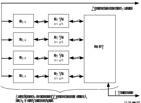
Data rates (a measure of baseband processing requirements), and partitioning of algorithms are given in Figure 1.
DUAL PORT MEMORY
SIMPLIFIES WIRELESS
BASE STATION DESIGN
APPLICATION
NOTE
AN-409
Figure 1. Baseband processing requirements[1]
DSP
DSP
DUAL PORT
DUAL PORT
DUAL PORT
DUAL PORT DSP
DSP
FPGA
Channel Decoding System
4 Antennas Base-band Processing: Channel Estimation,
JD, Smart Antenna, etc 6481 drw02
One of the most flexible architectures, with low cost and power requirements, is an array of DSPs or a “DSP farm”. In this architecture, an FPGA resides in the middle of the DSP array to perform heavily mathematical signal processing functions, such as chip-rate processing. This is very flexible in the way it can adapt to new standards. New heavily mathematical operations can be easily implemented in the FPGA, and if a more powerful DSP becomes available, the function can be absorbed back into the DSP. Using the FPGA as a switch enables DSPs working together to communicate with each other.
In baseband processing, another need is large memory space[4].
Both FPGAs and DSPs generally have limited on-chip memory, and price increases exponentially with on-chip memory size. Performance also decreases, especially for FPGAs, as more on-chip memory is added.
Since FPGAs and DSPs usually have different Input/Output (I/O) speeds and requirements, communications and buffering of data in the FPGA can drastically increase design complexity. This suggests that a communication device be placed between the DSPs and FPGA.
A dual ported memory[7] is the most suitable device for communication
between two asynchronous (different I/O speed) devices, such as a DSP and FPGA. In addition, both devices may use dual port memories as storage, memory and/or cache. Combining DSPs, dual port memories, and an FPGA result in a generic and flexible implementation of a baseband processor as shown in Figure 2.
An alternative would be to use fast memory like quad data rate synchronous RAM (QDR SRAM) (directly connected to an FPGA). Although this would be a cheaper solution, more latency is experienced in the FPGA to DSP data transfer.This solution also does not support asynchronous interface operation between different devices.
Here we investigate the performance, design area, and cost tradeoffs of different configurations, which use FPGA, DSP, and dual port memories, without necessarily focusing on a specific algorithm. Simula-tion results of different FPGA dual port memories in the architecture will be given, as well as proto-board experimental results.
EXPERIMENTAL ENVIRONMENT
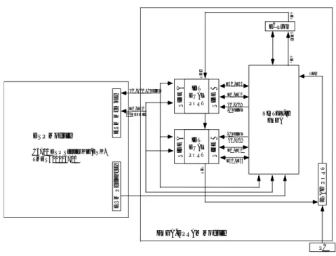
To study the DSP-farm's architecture and observe trade-offs in the architecture, we built a simple “DSP-farms lite” board. This architecture consisted of a TI C6711 starter kit connected through its external memory interface (EMIF) connector to a custom-built FPGA-DPRAM (Dual Port RAM) board (Figure 3).
The FPGA-DPRAM board consists of a Xilinx Virtex-II XC2V1000 along with two IDT 200MHz Dual Ports (DP). To make the design flexible, the dual ports were connected to the EMIF interface on the A-side and the FPGA on the B-A-side. The FPGA was also directly connected to the EMIF interface. This let us compare the system performance with and without the dual ports.
A bank of five user-function-LEDs were connected to five available I/O’s on the FPGA. These indicate “RUN”, “STOP”, “PASS”, “FAIL”, and “READY” status. We used these lights to indicate the state of the test. An Agilent 81110A pulse generator was used to vary the clock frequency. The FPGA was made to write and read patterns into its internal memory and external dual port. We compared the FPGA timing simulation results with the board experiment results.
Because the dual port helps these devices work asynchronously, we also looked at the DSP-dual port and the FPGA-dual port pairings and trade-offs separately.
Figure 2. Basic architecture of a flexible bseband processor in TD-SCDMA line card. FPGA receives signals from RF receiver system.
3
DSP Module C6711 DSP Starter Kit (DSK) TMDS320006711 E V M P e ri p h e ry E V M M e m o ry IDT DUAL PORT IDT DUAL PORT S ID E A S ID E A S ID E B S ID E B VIRTEX-II FPGA J T A G P O R T PC D32 - D35
D32 - D35
D0 - D31 D0 - D31
A0 - A19 A0 - A19 +Control
+Control
E2Prom
TD O TD O TDI T D I TD I T D O
A2 - A21 +Control
D0 - D31
FPGA-DPRAM Module 100MHz Max
6481 drw03
A dual port memory is a static memory core with dual access ports. Each port has separate address, data, and control signals for the core. A dual port can be used to connect two devices running at different interface frequencies, i.e., operating asynchronously. The advantage of a dual port is that the data is accessible by either port in a random fashion, with no constraints. Both ports are standardized SRAM interfaces, thus a dual port memory can be easily configured for FPGA or DSP use. The hardware connection is glue-less, typically requiring simple connections to the appropriate address, I/O, and control lines.
Using a dual port isolates the clock domains of the DSP and the FPGA. Isolating the clock domains allows the DSP to independently process raw data and pass resultant data while the processor on the opposite port loads additional raw data or receives the resultant data. Alternatively, if the system designer uses a SRAM, clock domains cannot be isolated, and memory access arbitration may increase the complexity in the FPGA/ASIC design or in the DSP software implementation.
DSP/DUAL PORT OVERVIEW
Texas Instrument’s (TI) TMS320C6000 Series DSPs may directly access an external dual port through the external memory interface (EMIF). The EMIF is easily configured to access many types of memories such as asynchronous and synchronous SRAM, SDRAM, and ROM. It has standardized address, I/O, and control buses for simple connection to the EMIF aforementioned memories. In many designs like “DSP-farms” it is not only used for data transfer, but is also used as the control plane (messaging). Please refer to the TI website for appropriate application notes[5].
The DSP works very well for pipelined algorithms, but bit-level parallelism is not exploited well by DSPs. Storage of bits as bytes in the DSP also results in significant overhead[6]. Furthermore, the compiler
may not take advantage of the fact that most multiplications are bit multiplications and may not replace them with additions or subtractions; high bit rate and parallel capabilities keep DSPs from replacing the FPGAs or ASICs[7].
To solve high bit rate requirements, the solution is to use multiple DSPs. Apart from cost and power drawbacks, this raises the difficulty in coordination between multiple processors because DSPs have limited switching capabilities. This can be resolved by using an FPGA as a switch between multiple DSPs. External accesses for the DSP have unpredictable execution times, and in the next section we will identify DSP external access latencies.
Direct Accesses Degrade DSP Performance
The major disadvantage of accessing the dual port directly from the DSP is the inherent latency incurred. The DSP stops while waiting for an external read or write instruction to complete, which may take many clocks. Thus, any processing that may be occurring is temporarily stopped. One alternative is to use the cache on the DSP, but execution times are unpredictable.
The theoretical DSP asynchronous direct memory access stalls for the board in Figure 3 for a single load (read) instruction is seven cycles, with an additional seven required for the CE_Read_Hold (chip enable should stay high for 7 clock cycles after the read instruction) (14 total cycles). Similarly, for a single write instruction six cycles are required for the store instruction itself, with an additional 4 for the CE_Write_Hold (chip enable should stay high for 7 clock cycles after the write instruction) (10 total cycles).
Figure 3. Top level block diagram of DSP and FPGA-DPRAM modules
WHAT ARE DUAL PORT MEMORIES?
LOAD (Read) # Clocks
STORE (Write) # Clocks Theoretical 14 10 Experiment 15 12
6481 tbl01 100.0% 90.0% 80.0% 70.0% 60.0% 50.0% 40.0%
0 256 512 768 1024 1280 1536 1792 2048 2304
6481 drw04
Frame Size (32-bit Dataword)
B W E ff ic ie n c y
Thus, if we assume the DSP is running at 100MHz, we will likely incur best case ~140ns delay for read instructions, and ~100ns for write instructions to the dual port. Using simple C code, which had loops of back-to-back read and write instructions, we noted approximately the same values. To help reduce the delays incurred by these stalls, we have to avoid performing direct external memory accesses.
Improve Bandwidth and Reduce DSP Stalls with
Direct Memory Access (DMA)
DSP stalls incurred by direct accesses to the external dual port can be avoided by instead using the DSP DMA.
The DMA provides a second, independent state machine to handle batch reads and writes from an external memory. For example, this batch processing is ideal for FFT processing. The accesses still are performed across the standard EMIF interface, so the same standard connection and configuration may be used to access the dual port. The DMA transfers the dual port’s data to the DSP’s on-chip data memory. The internal data memory is optimized for high-speed direct access by the DSP.
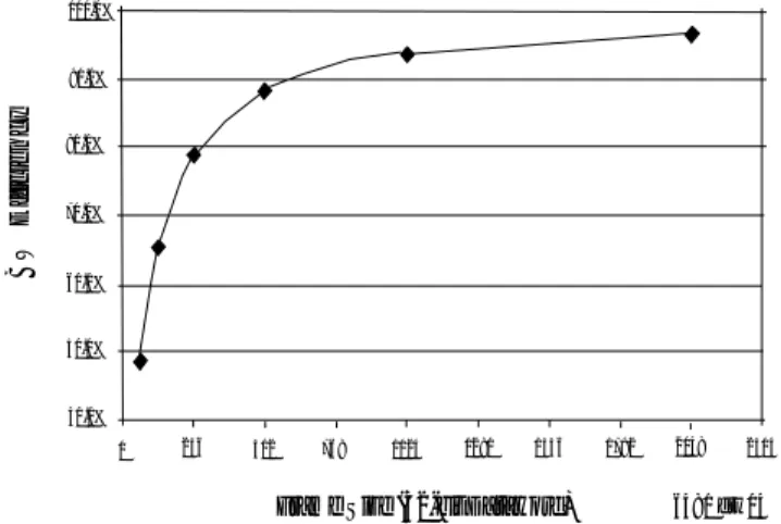
Because of the latency involved in starting a DMA transfer, large block transfers are recommended in order to maximize DMA bandwidth efficiency. Using a dual port memory allows large blocks of data to be completely buffered in dual port memory prior to transfer to or from the DSP, and performance is increased such that one data word is transferred for every EMIF cycle.
We can determine the bandwidth efficiency for a given frame size for a typical event-driven DMA transfer from the dual port to the DSP's internal data memory. This would typically take six cycles for synchronizing the DMA, two cycles read instruction latency for the dual port, forty cycles for the DMA to start the read, and twenty cycles to start the write (approximately 68 cycles total).
The bandwidth is about 80 percent utilized at 256-word frame length where each word is 32 bits. The size of unspread 3G-frames is from 160 bits (20 bytes) to 10240 bits (1280 bytes). If the FPGA handles the chip rate processing, it will hand off unspread data to the DSP. Transfers of more than 256 bytes should be used if possible in order to best utilize available bandwidth. In the case of a 3G spread-frame size of 40960 bits, 5120 byte transfers may be used so that the frame can be completely stored in dual port memory during processing.
Typically, the DSP CPU can perform read and write accesses to the internal data memory on a per cycle basis. This can be further optimized to two simultaneous accesses per clock cycle. The only caveat is if the DMA and the DSP CPU try to simultaneously access the same memory location. Even under this condition, only one to two cycle stalls will incur.
For our experiment's board access performance comparison, we again used the simple memory-access code. The code was simply modified to have the memory pointer point to the on-chip data memory rather than the external dual port. The code ran approximately two times as fast for the DSP to data memory compared to that of the direct DSP to dual port access.
Bandwidth is optimized when the DMA is performing transfers of new or resultant data simultaneous to the DSP CPU performing its operations. If the user takes advantage of this parallel architecture, it is likely in most applications that the DMA will stream enough data to keep the DSP CPU busy. That is, the program operations will likely determine the bandwidth of the overall system. This is an important feature for the DSP programmer, because the stalling to wait for memory results would affect the overall system performance.
Dual Port Adds Buffer for DSP Performance
The dual port acts as a buffer for the DSP, which is particularly useful for increasing performance. Dual ports are currently offered in densities up to 18Mb (~2MB). This is greater than the maximum data memory space available in most DSPs. The greater buffer space in a dual port is a major strength of using the DSP – dual port pairing.
Dual Port Splits Clock Domains to Maximize DSP Performance
As stated in Rajagopal et al.[6], a single DSP will not be enough
even for the channel estimation portion of baseband processing. This paper shows that going from 1 to 2 DSPs increases the performance from 1.19-5.92 times for varying number of users, but programming two DSPs to work simultaneously is a challenging task. By inserting a dual port in between DSPs, the clock domains and execution times of DSPs are separated from each other, which simplifies the software design. Doing smaller (byte-by-byte) external memory access from the DSP is not effective. DSP algorithms should work on large chunks of data that are small enough to fit the DSP's internal memory. Since DSPs are not good at parallel operations like matrix operations, and since these operations require a lot of memory, these algorithms should be realized by a custom ASIC or FPGA.
Figure 4. Bandwidth efficiency vs. effective frame size of DSP EMIF interface whil using the DMA
Table 1. Theoretical and experimental results for direct read and write to external memory latency
5
6481 drw05
FPGA-DP OVERVIEW
The programmability of the FPGA makes it an ideal candidate for baseband processing. Since standards and algorithms are changing continuously, they can be easily implemented with a DSP/dual port/ FPGA chain. The FPGA is responsible for chip rate processing and is very effective for parallel operations like matrix multiplication, inversion, etc. The designer will then face the question: How much memory should stay in the FPGA, and how much should go outside to the dual port?
Performance Trade-offs
To analyze the affects of utilizing the FPGA dual port memory we simulated the change in speed, area, and power performance by embedding dual port memory in the FPGA using Xilinx's Integrated System Development Tool. The results were compared against the board experiment results.
Figure 5 is the template for the simulation of the dual port function set-up within the FPGA. For increasing amounts of internal dual port memory, internal speed, set-up time, and maximum speed were measured. Maximum speed was compared to the results from the board experiment. The internal speed indicated how quickly information could be directly written into and read from the dual port core block in the FPGA. Setup time was the minimum data arrival time to the dual port core in the FPGA before the clock. Clock-to-pad was the minimum output time required after the clock. To compare against the external dual port, we pipelined the outputs (FF in Figure 5), but not the inputs.
We used the optimized dual port core from the Xilinx Core generator tool. Performance benchmarks were based on post-layout timing analysis. Since cores in the Core Generator tool are layout-optimized, the performance was predictable and repeatable. We compared the external dual port against the dual port core (not SRAM core) in the FPGA. The dual port core should show the same features, like clock isolation, as the external dual port, although the second port may not be connected to an outside ASIC but may be connected to an internal module. Place and route was performed through software with no further optimization.
Figure 5. FPGA internal memory performance measurement template
Maximum Speed = Minimum {Internal Speed, External Speed} External Speed = 1/{Clock-to-PAD+ transmission line delay+
Setup time of neighbor ASIC}
For all of the simulations, transmission line delay (only three inches of 0.01-in. 1-oz copper trace between the ASIC and the FPGA) was minimal and hence was ignored. Setup time of neighbor ASIC was taken as the setup time of the FPGA assuming that the FPGA was connected to a similar FPGA.
Performance Results
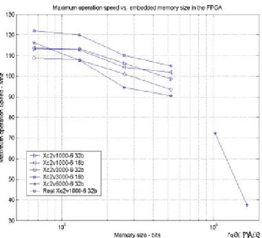
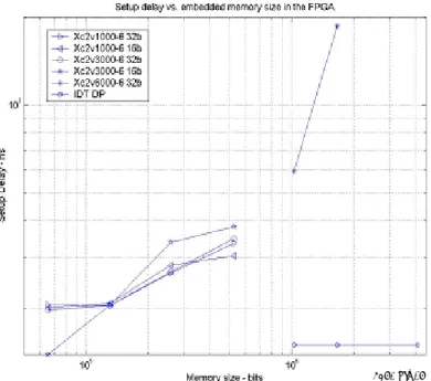
Figure 6 to Figure 9 show the internal speed, setup time, maximum speed, and estimated worst case power consumption of the simulated dual port for the Xilinx XC2V1000-6, XC2V3000-6, and XC2V6000-6 with increasing memory size from XC2V6000-65Kbits to 1.5Mbits.
The speed drops significantly around the 256Kbit point as the memory interconnect delays start to take significant effect. This is due to the timing delays associated with the length of the logic interconnections between the dual port core in the FPGA. Figure 8 also includes the board experiment results. Observe that the frequency at which the hardware setup exhibited failure is comparable to the simulation results. All of the plots (Figure 6 to Figure 9) show that the internal FPGA routing may have a nonlinear effect on the overall speed performance of the system. A 16-bit wide data path dual port core has better overall speed performance for smaller embedded DP memories compared to a 32-bit one, but as more memory is embedded, the routing of memory blocks to 32 pins is easier compared to 16 bits. Although the maximum speed (Figure 8) was around 90MHz for 500Kbit dual port core, it dropped to 40MHz for a 1.6Mb dual port core embedded in the 6-million gate FPGA.
Another important observation is that setup and clock to pad delays become the limiting factor in the overall system performance. Since we do not buffer at the input, the setup time gets larger as more dual port
6481 drw06
6481 drw07
Figure 6. Internal speed vs. dual port core size
7
6481 drw08
6481 drw09
Figure 8. Maximum speed (simulation and experiment) vs. dual port core size results
Figure9. Dissipated power vs. dual port core size simulation results
72 144 432 576 720 1,728 2592 3,024 Memory (Kbits)
0 200 400 600 800 1000 1200
1400 Virtex-II Package Sizes
Packag
e
Siz
e
(s
q
.
mm)
6481 drw12
FPGA family and the equivalent external dual port. Note that the memory cost per bit of the dual ports actually decreases as the memory increase. The memory cost per bit for the FPGA starts to increase above 256K. This graph clearly shows that FPGA memory is some of the most expensive memory available.
Design complexities of optimizing FPGA performance
Optimizing the FPGA code requires a significant amount of experience due to routing constraints. For example, if the same amount of logic and memory is implemented a bigger FPGA will be slower than a smaller one, and significant optimization of HDL code is required to achieve the performance desired.
Comparison of packages for board space issues
Figure 11 shows the FPGA package size as it relates to the amount of memory available in the FPGA. Using a larger FPGA just for the increased memory may not be the best idea. For smaller memory requirements, the FPGA package size may be sufficiently small. However, greater memory density requires much larger packaging. For example going from 720Kbits of memory to 1728Kbits of internal dual port core, the total area of the FPGA increase by 650mm2. If the same memory is
exported to dual ports, the total package size increment is 300mm2.
memory is embedded in the FPGA. Although this is smaller than the internal delay, for overall system performance we have to take the clock-to-pad delay of the neighbor ASIC into account. Summation of setup and clock-to-pad delay gives us maximum latency in the system.
If the same memory size is embedded in two different sized FPGAs, the smaller FPGA will have better speed and power performance. The maximum speed plot shows that a 32-bit data path, 3 million-gate FPGA is 10MHz slower than a 1-million gate FPGA. Furthermore, dissipated power increases from 698mW in the 1-million gate FPGA to 978mW in the 6-million gate FPGA for 500Kbit dual port core. No other logic or memory was embedded in the FPGA.
Note that the setup time for the external dual port is constant at 1.5ns and for most of the memory usage range it is significantly lower than any of the FPGA. The maximum speed of the external dual port is 200MHz (not shown on Figure 8). Hence this is much faster compared to the same size embedded dual port on the FPGA.
Baseband processing algorithms such as parallel interference cancellation (PIC) for pilot synchronization in 3G base stations may need more than 7Mbit of memory alone (Table2)[8] . So it may be more
beneficial to move this memory to an external dual port and let the FPGA handle the parallel multipliers and adders by accessing the data from the external dual port. The external dual port will be able to run at 200MHz. The FPGA will also speed up because of less routing, and it can be replaced with a smaller size FPGA, which further increases the performance.
Another prohibitive factor for the FPGA is cost. Figure 10 shows the relative memory cost per bit comparison between the Xilinx Virtex II
Figure 11. Board space comparison of IDT DP vs. the FPGA
Figure 10. Relative cost of FPGA vs. dual port memory Table 2. 3G parallel interference cancellation (PIC)
algorithm memory requirements[6]
CONCLUSION
In this paper, we discussed memory trade-offs in a flexible DSP/ dual port/FPGA architecture. DSP's cannot handle the parallel operations needed in chip-rate processing, so an FPGA is needed to off-load these functions and to work as a switch between multiple DSPs. A dual port is a vital device between the DSP and the FPGA, as it isolates two devices from each other thereby simplifying design.
Spreading Factor Number Users Bits of Memory
32 32 112,000 32 32 811,264 256 256 7,350,272
Cost
256-Pin 1.0mm BGA 456-Pin 1.0mm BGA 676-Pin 1.0mm BGA 896-Pin 1.0mm BGA 1152-Pin 1.0mm BGA IDT 256-Pin 1.0mm BGA
6481 drw11
9
REFERENCES
[1] S. Sriram. 3G Cellular Baseband Design. BWCR, September 2000 [2] S. Morris. Signal-Processing Demands Shape 3G Base Stations.
Wireless System Design Magazine 12-18, November 1999
[3] J. Lee, J.Chung, K. Kim, Y. Jeong, K.Cho. Implementation of the Wideband CDMA Receiver for an IMT-2000 System. IEICE
Trans. on Commummunications. VOL. E84-B, NO. 4, Pages
709-715, April 2001
[4] J. Das, S. Rajagopal, Arithmetic Acceleration Techniques for Wireless Communication Receivers. 33rd Asilomar
Conference on Signals, Systems and Computers. Pages
1469-1474, Pacific Grove, CA., October 1999 [5] TI DSP Products, www.ti.com
[6] S. Rajagopal, B.A. Jones, J.R. Cavallaro. Task Partitioning Wireless Base-Station Receiver Alorithms on Multiple DSPs and FPGAs. ICSPAT. Dallas TX., October 2000
[7] Rupert Baines, Doug Pulley. A Total Cost Approach to Evaluating Different Reconfigurable Architectures for Baseband
Processing in Wireless Receivers. IEEE Communications
Magazine. Pages 105-113, January 2003
[8] S. Rajagopal, S. Bhashyam, J.R. Cavallaro, B. Aazhang. Efficient VLSI Architectures for Baseband Signal Processing in Wireless Base-Station Algorithms. Rice University Center for Multimedia
Communication, 2000
Since DSPs are pipelined devices, data transfer from and to the DSP should be done in frames. We found that packets larger than 256 bytes utilize the dual port-DSP bandwidth efficiently. Dual ports can act as a buffer not only to the DSP but also to the FPGA.
We have demonstrated when dual port memory should be moved external to the FPGA. The FPGAs have dual port cores that are available as soft intellectual property. Performance simulations have shown us that as more memory is incorporated in the FPGA, overall performance of the system drops significantly. Dual port memories larger than 256 Kbits should be exported to the external dual port, because of power, speed, cost and design complexity issues.
The IDT logo is a registered trademark of Integrated Device Technology, Inc.
CORPORATE HEADQUARTERS for SALES: for Tech Support:
6024 Silver Creek Valley Road 800-345-7015 or 408-284-8200 408-284-2794 San Jose, CA 95138 fax: 408-284-2775 [email protected]
![Figure 1. Baseband processing requirements [1]](https://thumb-us.123doks.com/thumbv2/123dok_us/8569301.2320901/1.918.210.700.687.1040/figure-baseband-processing-requirements.webp)

![Figure 10. Relative cost of FPGA vs. dual port memoryTable 2. 3G parallel interference cancellation (PIC)algorithm memory requirements[6]](https://thumb-us.123doks.com/thumbv2/123dok_us/8569301.2320901/8.918.111.425.791.1064/figure-relative-memorytable-parallel-interference-cancellation-algorithm-requirements.webp)
