TIME DELAY MEASUREMENT AND VOLTAGE REFERENCE CIRCUITS COMPATIBLE FOR EMBEDDED TEST IN 3D STACKED ICS
By
SHADI M. HARB
A DISSERTATION PRESENTED TO THE GRADUATE SCHOOL OF THE UNIVERSITY OF FLORIDA IN PARTIAL FULFILLMENT
OF THE REQUIREMENTS FOR THE DEGREE OF DOCTOR OF PHILOSOPHY
UNIVERSITY OF FLORIDA 2010
© 2010 Shadi M. Harb
To my wonderful mom, my great dad, my dear wife, my sweet brother and sisters
ACKNOWLEDGMENTS
I would like at this opportunity to thank everybody who helped me and support me to make my dissertation possible.
First, I would like to express my sincere appreciation to my PhD advisor, Professor William R. Eisenstadt, for all his generous supports and guidance throughout my PhD journey as graduate student. It has been my great pleasure and honor to work with Professor Eisenstadt towards my PhD degree.
I would like to give a special thank to my co-advisor professor Robert M Fox; I cannot express in words the importance of his involvement in my graduate career. I would really appreciate all the academic advising and the valuable suggestions and comments from the idea proposal to its realization.
I would like also to thank Professors John G. Harris, Fan Ren, and Bruce A. Welt for their advice in this work and their willing service on my committee. I am grateful to Dr. Rizwan Bashirullah, Dr. Jenshan Lin and their students who allowed me to access the test equipment whenever needed.
My special appreciation and thanks also go to my great manager at Intel Corporation, Bob Bock, for his understanding, patience, support, and help.
Finally, and importantly, I would like to thank my parents for their support when I faced choices. A very special thank my Mom, who has always been with me throughout all the challenges and struggles in my life, and without whose live, support, and
inspiration, I would never be what I am today. Above all, I would like to thank my God for being supporting me for every walk in my life and for the blessings that he gave me throughout my life. Also I am grateful to my wife, Sahar Alhaj-Ali. Her love, help and support have been essential to the fulfillment of this work.
TABLE OF CONTENTS page ACKNOWLEDGMENTS ... 4 LIST OF TABLES ... 8 LIST OF FIGURES ... 9 ABSTRACT ... 16 CHAPTER 1 INTRODUCTION ... 18
1.1 Three Dimensional Integration Technologies ... 18
1.1.1 General 3D Integration Technologies ... 21
1.1.2 Potential Drivers for 3D Technology ... 24
1.1.3 Applications and Designs using 3D Technology ... 26
1.1.4 Merits and Advantages of 3D Circuits ... 28
1.1.5 The Challenges of Adopting 3D Technology ... 32
1.1.6 Limitations and Concerns in 3D Technology ... 33
1.1.7 MIT Lincoln Lab 3D Integration Technology ... 35
1.1.7.1 MIT 3DM3 integration process ... 35
1.1.7.2 Thermal consideration in MIT 3D stacked ICs process ... 39
1.1.7.3 MIT 3D stacked ICs testing during procession ... 40
1.2 Challenges of High Speed 3D IC Test ... 41
1.2.1 IC Testing Cost ... 41
1.2.2 Time Involved in IC Testing ... 43
1.2.3 Test Challenges in 3D Integrated Circuits ... 43
1.3 Embedded Test as a Potential Solution ... 45
1.4 Organization of the Dissertation ... 46
2 SIGNAL INTEGRITY AND THERMAL EFFECTS IN 3D STACKED ICs ... 49
2.1 Introduction ... 49
2.2 Signal Integrity Effects in 3D Stacked ICs ... 50
2.2.1 Introduction to Common Signal Integrity Effects ... 50
2.2.2 Noise Coupling Effects in 3D Stacked ICs ... 53
2.3 The Benefit of I/O Characterizing in 3D Stacked ICs ... 54
2.4 Motivation and Contribution of this Work ... 55
2.5 Electrical Characterization of 3D Interconnect based on 3D Full Wave Simulator ... 57
2.5.1 3D Full Wave (HFSS) and Spice Type Circuit (ADS) Circuit Simulations ... 58
2.5.2 Structural Effects on Electrical Characteristics of 3D Vias ... 62
2.5.3 Crosstalk between 3D Vias ... 64 5
2.5.3.1 The influence of 3D via dimensions on crosstalk ... 64
2.5.3.2 3D via crosstalk in structures with different configuration ... 66
2.6 Thermal Effects in 3D Stacked ICs ... 69
2.6.1 A Simplified Thermal Model for 3D Stacked ICs ... 70
2.6.2 Thermal Estimation in 3D Stacked Chips using the Thermal Analysis Tool (FloTHERM) ... 71
3 A CMOS VOLTAGE REFERENCE GENERATOR ... 73
3.1 Introduction ... 73
3.2 The Proposed Voltage Reference ... 77
3.3 Analytical Study of the Proposed Voltage Reference ... 79
3.3.1 Design Analysis ... 79
3.3.2 Temperature Compensation ... 81
3.3.3 Design Requirements ... 83
3.4 Circuit Design and Implementation ... 84
3.4.1 Circuit Topology with On-chip Trimming ... 84
3.4.2 Stability Analysis ... 86
3.4.3 Power Supply Rejection ... 89
3.4.4 Circuit Performance and Results ... 91
3.5 Summary and the Contribution of this Work ... 93
4 EMBEDDED HIGH RESOLUTION TIME DELAY MEASUREMENT ... 99
4.1 Introduction ... 99
4.2 The Basic Techniques in Time Measurement ... 99
4.2.1 Tapped Delay Lines ... 99
4.2.2 Vernier Delay Line ... 101
4.3 Proposed High Resolution Delay Generator ... 102
4.4 Proposed System Architecture for Embedded Time Delay Measurement ... 103
4.5 Simulated and Measured Results ... 108
4.6 Summary and the Contribution of this Work ... 111
5 A HIGH RESOLUTION CMOS MULTI-EDGE DELAY GENERATOR ... 117
5.1 Introduction ... 117
5.2 Sub-gate Timing Resolution Using Vernier Delay Line (VDL) ... 118
5.3 A Novel Multi-Edge Vernier Delay Generator ... 121
5.4 Circuit Performance and Results ... 125
5.5 Summary and the Contribution of this Work ... 128
6 ON-CHIP SELF-TESTING (BIST) TECHNIQUES FOR 3D STACKED ICs ... 135
6.1 Introduction ... 135
6.2 An Equivalent Electrical Circuit Pi-Model for Through Silicon Vias (TSVs) ... 136
6.3 Proposed Testing Strategy for 3D IC Characterization ... 138
6.3.1 3D GTL I/O Test ... 139
6.3.1.1 Single-ended gunning transceiver logic (GTL) I/O design ... 139 6
6.3.1.2 GTL circuit architecture in 3D stacked ICs ... 140
6.3.2 3D TSV Time Delay Measurement ... 144
6.3.3 Temperature Sensors for 3D Thermal Characterization ... 145
6.3.3.1 Background on the diode-connected temperature sensors ... 146
6.3.3.2 Circuit design of the temperature sensor biased by the voltage reference circuit ... 148
6.4 3DTest for Crosstalk Induced-Delay and Glitches ... 152
6.5 3D TSV Test using the GTL I/O Shift Register as Scan Chain ... 154
6.6 Oscillation Ring (OR) Based 3D Interconnect Test Architecture ... 156
6.6.1 Oscillation Ring (OR) Test ... 156
6.6.2 Proposed Oscillation Ring (OR) 3D Test Methodology Using the Multi-Edge Delay Generator ... 157
6.6.2.1 TSVs test with different configurations ... 157
6.6.2.2 TSV rise time degradation test ... 160
6.6.2.3 TSVs crosstalk test ... 162
6.7 Summary and Contribution of this Work ... 164
7 SUMMARY AND FUTURE WORK ... 168
7.1 Summary ... 168
7.2 Suggested Future Work ... 169
APPENDIX A APPLICATIONS FOR THE PROPOSED DELAY GENERATOR ... 171
A.1 Sampling Clock Generator (SCG) ... 171
A.1.1 Sampling Clock Generation Architectures ... 171
A.1.2 High Resolution SCG using the Proposed Delay Generator ... 173
A.2 High Speed Real-Time Samplers ... 178
B PHASE INTERPOLATORS TO IMPROVE THE SAMPLING RESOLUTION OF THE PROPOSED DELAY GENERATOR ... 179
B.1 Introduction to Phase Interpolators ... 179
B.2 Types of Phase Interpolators ... 180
B.2.1 Single-Ended CMOS Phase Interpolators ... 180
B.2.2 Differential CML Phase Interpolators ... 182
LIST OF REFERENCES ... 185
BIOGRAPHICAL SKETCH ... 193
LIST OF TABLES
Table page
1-1 Potential drivers for 3D integration ... 26
1-2 The metal layers of the 3DLAND and doughnut feature for each tier ... 39
3-1 Typical DC voltages for the implemented voltage reference ... 85
3-2 Measured performance for the voltage reference ... 93
3-3 Comparison between this work and published work in literature ... 93
4-1 Eight-state finite state machine ... 108
4-2 Comparison between this design and previous works in literature ... 112
5-1 Jitter performance for the delay generator at difference noise frequencies ... 125
5-2 Comparison between this work and different timing generators in literature .... 130
LIST OF FIGURES
Figure page
1-1 Interconnect roadmap ... 18
1-2 A simple illustration of a 3D stacked IC with TSVs ... 19
1-3 Schematic of a 3-D chip showing heterogeneous technology integration ... 21
1-4 3D stacking geometries ... 22
1-5 Illustration of vertical interconnect technologies ... 24
1-6 Wire reduction due to 3D routing ... 25
1-7 Improvement in path delay achieved using 3D technology vs. technology scaling alone ... 27
1-8 (a) Planer floorplan of a deeply pipelined x86 microprocessor, (b) 3D floorplan of a deeply pipelined x86 microprocessor ... 29
1-9 3D network-in-memory architecture ... 30
1-10 (a) 3D image architecture, (b) Mapping of a single pixel circuit on 3D layers ... 31
1-11 Cross-sectional views of matchline TCAM, (a) Conventional 2D with single tier, (b) 3-tier 3D TCAM design ... 31
1-12 Three-dimensional implementation of FPGAs with 3D routing switches ... 32
1-13 Coupling effects in 3D technology ... 34
1-14 Heat flow in 3D technology ... 34
1-15 The 3D process flow ... 37
1-16 Thickness stack for three-tier structure with actual layer thicknesses ... 38
1-17 Moore’s law for test: fab vs. test capital ... 41
2-1 Crosstalk mechanism: (a) Capacitive crosstalk (b) Inductive crosstalk ... 52
2-2 Near-end crosstalk (NEXT) and far-end crosstalk (FEXT) ... 52
2-3 The VDD and ground noise ... 53
2-4 A conceptual view for 3D stacked ICs on-chip test ... 56
2-5 Structure of 3D via for 3D full wave simulator ... 58 2-6 Simulation of high speed TSV properties ... 59 2-7 Evaluated S21 magnitude (a) and S11 magnitude (b) of 3D via using HFSS ... 59
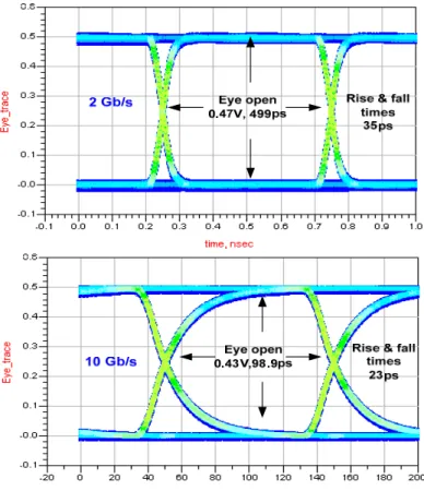
2-8 The simulated eye-diagrams of 2Gbps (a), and 10 Gbps (b) PRBSs after
passing through the 3D via ... 60 2-9 Eye diagrams for stacked 3D vias ... 61 2-10 S21 magnitudes of 2, 5, 10, and 20 stacked 3D vias associated to the graphs
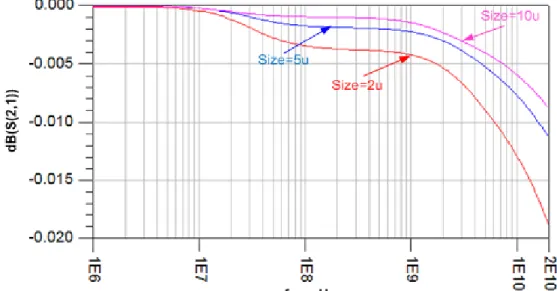
from top to bottom respectively ... 62 2-11 Evaluated S21 magnitudes for size of 2 µm, 5 µm, and 10 µm associated to
the graphs from bottom to top respectively ... 63 2-12 Evaluated S21 magnitudes for height of 4µm, 7µm, and 17µm associated to
the graphs from top to bottom respectively ... 63 2-13 Evaluated S21 magnitudes for Via pitch of 5µm, 20µm, and 50 µm associated
to the graphs from bottom to top respectively ... 64 2-14 Location of signal vias and GND vias for crosstalk evaluation, (a) SGSG, (b)
SGGS configurations ... 64 2-15 Comparison of five locations of 3D vias. The distances 4 µm, 8 µm, 16 µm,
and 32 µm between two signal vias are associated to the graphs from top to bottom respectively ... 65 2-16 Comparison of three locations of GND Vias. The distances 4 µm, 8 µm, 16
µm, and 32 µm between two GND vias are associated to the graphs from
bottom to top respectively ... 66 2-17 Comparison between SGSG and SGGS configurations for 10 µm distance,
SGSG and SGGS are the top and bottom graphs respectively ... 66 2-18 Comparison of three different configurations, (a) Configuration #1, (b)
Configuration #2, (c) Configuration #3, and (d) Configuration #4 ... 67 2-19 Crosstalk between four different configurations ... 68 2-20 A TSV coupling model that includes the transmission lines ... 68 2-21 Comparison of crosstalk between TSVs with and without the inclusion of
transmission lines ... 69 2-22 (a) A 3D IC with n layers, (b) Equivalent thermal circuit for 3D stacked ICs ... 70
2-23 Maximum Temperature vs. number of stacked TSV chips ... 72
3-1 An example of a self-biased (Bootstrapped) current reference ... 74
3-2 The general principle of bandgap reference ... 75
3-3 Typical bandgap reference circuit in CMOS technology ... 75
3-4 De Vita’s Voltage Reference... 78
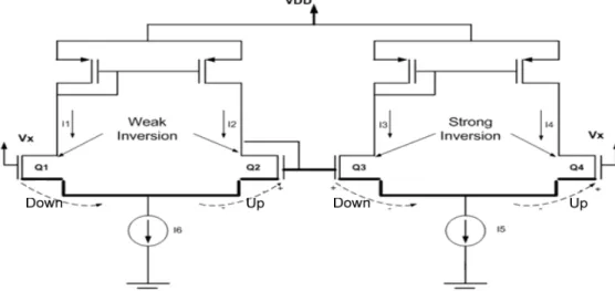
3-5 The proposed voltage reference topology with “up-down-up-down” configuration ... 79
3-6 The proposed voltage reference circuit with a translinear Loop ... 81
3-7 The proposed voltage reference circuit with self-biasing ... 84
3-8 Schematic for the proposed voltage reference ... 85
3-9 Schematic of the binary to thermal code inverter ... 85
3-10 The layout of the voltage reference, (a) Core circuit, (b) Whole layout ... 86
3-11 Loop gain and phase with respect to frequency ... 87
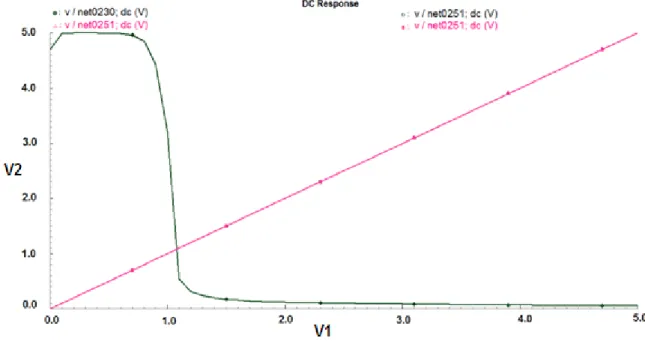
3-12 The first test setup, which breaks the main common loop in the circuit ... 88
3-13 Large signal sweep (V2 vs. V1) plot showing only one operating point ... 88
3-14 The second test setup, which breaks all possible loops in the circuit ... 89
3-15 Output currents of the sources (V1 &V2) with respect to the large signal sweep of V2 ... 89
3-16 Small signal analysis for power supply noise using the right side of the proposed circuit ... 90
3-17 The output voltage reference as a function of temperature (~ 0.26mV variation) ... 91
3-18 Chip microphotograph ... 92
3-19 Photo of the packaged die ... 92
3-20 Measurement setup using temperature control oven ... 92
4-1 Simple delay line measurement scheme ... 100
4-2 DLL block diagram ... 101
4-3 The Vernier delay line ... 102
4-4 The high resolution multi-edge delay generator... 103
4-5 Interconnect time delay measurement ... 104
4-6 Proposed embedded time delay measurement architecture ... 105
4-7 Modified version of the proposed embedded time delay measurement architecture ... 106
4-8 Sampling timing diagram ... 107
4-9 Current starved delay element ... 109
4-10 Simulated waveforms for the time delay measurement architecture ... 109
4-11 Whole layout of the proposed embedded time delay architecture ... 110
4-12 Measurement setup for the time delay architecture ... 110
4-13 Chip microphotograph ... 110
4-14 The measured counter outputs with respect to the input control voltage of the DUT ... 111
4-15 (a) Simple digital time delay measurement circuit, (b) Time delay measurement diagram ... 111
5-1 Absolute delay and relative delay ... 117
5-2 Sub-gate timing resolution VDL ... 119
5-3 Single-stage VDL ... 119
5-4 Circuit implementation of the fast and slow oscillators ... 120
5-5 (a) Simple delay element, (b) Current starved delay cell ... 120
5-6 Sub-gate Vernier delay generator using chains of delay elements ... 121
5-7 The proposed architecture of the multi-edge delay generator ... 123
5-8 Modified version for the proposed architecture of the multi-edge delay generator ... 124
5-9 Simulated single-ended CMOS delay generator with a state-of-the-art 45nm technology and 1.1V supply voltage ... 125
5-10 The two triggered oscillators from the proposed architecture ... 126
5-11 The generated delay edges from the proposed architecture ... 126
5-12 (a) Delay generator layout, (b) Whole layout ... 127
5-13 Measurement and test setup ... 127
5-14 Chip microphotograph ... 127
5-15 Measurements of the time delay generator ... 128
5-16 Delay versus control voltage (vctr_slow) (AMI 0.5µm process, Vdd=5V) ... 128
6-1 Equivalent Circuit Model of a Standard GSG TSV ... 137
6-2 Equivalent Circuit Model of a Standard GSSG TSV ... 137
6-3 3D BIST System ... 138
6-4 A GTL I/O test structure ... 139
6-5 The GTL I/O test structure in 3D stacked IC ... 140
6-6 3D GTL I/O Circuit Implementation ... 141
6-7 Measuring crosstalk between TSVs in 3D stacked IC ... 142
6-8 3D GTL I/O test using ADS... 142
6-9 Simulated 3D GTL test results at 1Gb/s data rate ... 143
6-10 3D layout for the GTL I/O test ... 143
6-11 A U shape interconnect time delay measurement ... 144
6-12 An example of 3D interconnect time delay measurement ... 144
6-13 Schematic of the temperature sensor ... 147
6-14 The temperature sensor biased by the voltage reference circuit ... 148
6-15 Simulated transconductance characteristics of diode connected NMOS transistor ... 149
6-16 Simulated transconductance characteristics of PMOS transistor ... 150
6-17 The output of the voltage reference with respect to temperature (biasing voltage=0.641V) ... 150
6-18 The temperature invariant current for the PMOS FET with respect to
temperature (1.1µA variation) ... 151
6-19 The temperature sensor output (Vtemp) with respect to temperature ... 151
6-20 3D Interconnect crosstalk induced-delay test ... 152
6-21 Different crosstalk patterns ... 153
6-22 3D interconnect induced-delay crosstalk for different crosstalk patterns ... 154
6-23 3D interconnect induced-delay crosstalk cancellation ... 154
6-24 The GTL serial-to-parallel shifts register for 3D TSV test ... 155
6-25 An example of using the GTL shift register as scan chain ... 156
6-26 Outputs of the scan chain using the GTL shift register (a) with fault-free TSVS, (b) with faulty TSVs ... 156
6-27 3D interconnect test based on the multi-edge delay generator ... 158
6-28 3D test with different configurations ... 159
6-29 Output frequencies for the triggered oscillators ... 160
6-30 Output frequencies and counters values for different 3D configuration (a), 2 TSVs, (b) 4 TSVs, (c) 8 TSVs ... 160
6-31 TSV rise time (red: 45ps, blue: 1.3ns) ... 161
6-32 Output frequencies and counter values for (a) 45 ps TSV rise time, (b) 1.3 ns TSV rise time ... 161
6-33 3D crosstalk detection test based on the multi-edge delay generator ... 162
6-34 Test setup for 3D interconnect crosstalk ... 163
6-35 Simulated results for 3D interconnect crosstalk, (a) Crosstalk-coupled (b) Crosstalk-free ... 163
6-36 Output frequency for (a) Crosstalk-coupled and (b) Crosstalk-free oscillators . 164 7-1 Conceptual view of the 3D BIST system ... 170
7-2 Multi-edge delay generator for 3D interconnect characterization... 170
A-1 Traditional circuit architecture of the sampling clock generator ... 171
A-2 System with on-chip sampling clock generator ... 172
A-3 System with external sampling clock generator ... 173
A-4 The sampling system architecture I ... 174
A-5 The phase fine tuning levels ... 175
A-6 The phase select architecture ... 176
A-7 The sampling system architecture II ... 176
A-8 The sampling system architecture III ... 177
A-9 The four generated clock phases ... 177
A-10 Characterizing signal integrity effects using high speed samplers... 178
A-11 High speed real-time sampler using the proposed delay generator ... 178
B-1 Block diagram of a phase interpolator ... 179
B-2 Phase interpolation output waveforms ... 180
B-3 Single-stage phase-blender circuit ... 181
B-4 Two-stage, cascaded phase-blender circuit for 4x phase-resolution improvement ... 182
B-5 Phase interpolator implementation, Type I ... 183
B-6 (a) Phase interpolator implementation, Type II (b) Unit cell of type II phase interpolator ... 184
Abstract of Dissertation Presented to the Graduate School of the University of Florida in Partial Fulfillment of the Requirements for the Degree of Doctor of Philosophy
TIME DELAY MEASUREMENT AND VOLTAGE REFERENCE CIRCUITS COMPATIBLE FOR EMBEDDED TEST IN 3D STACKED ICS
By Shadi M. Harb
August 2010 Chair: William R. Eisenstadt
Cochair: Robert M Fox
Major: Electrical and Computer Engineering
3D Technology is emerging as an attractive way to sustain Moore’s law, by making it possible for highly integrated, high performance, cost effective compact structures. The key benefits of 3D ICs over traditional 2D chips include 1) reduction of the global interconnect length, which can reduce the time delay significantly between components and functional blocks, 2) high packing density, 3) smaller footprint, and 4) the
enablement of mixed-technology integration. However, a problem facing the industry now is in the testing of such stacked die devices after they have been stacked and packaged. Stacked ICs suffer from the same problem as multi-chip modules (MCMs), IC boards, and other integration schemes: one bad component can kill the system. As more components are integrated, the yield of the final product falls off exponentially. With the IC exposed, areas of interest in the IC become accessible for testing. However, in the case of a stacked device, there is more than one die. Thus, at least some of the electrical contacts of the lower dies are typically covered by the dies above them and cannot be accessed. Furthermore, it is not possible to isolate the characteristics of individual devices since the functioning of devices on one die is impacted by the devices
17
on the other dies, since the dies are interconnected to allow all of the dies to work as one large IC. Thus for aforementioned reasons, 3D IC testing has become more challenging, expensive and complicated. The cost of the ATEs for IC test is becoming more prohibitive, and the reliable high frequency testing has become a significant restrictive and influencing factor for the time-to-market of the IC industry. A more attractive solution to this problem, which has more potential to reduce the cost of
testing, is the embedded Buit-In-Test (BIT). This method helps to keep up with the pace of the growing complexity of tests. Embedded test reduces the time to production
without increasing the test cost and enables the use of low-cost testers, already on the factory floor, efficiently. However, there is some increase in chip die area and
production chip cost. The fundamental idea in this solution for 3D test is to provide a full embedded test solution in 3D stacked ICs by moving some of the external high-speed and high-bandwidth test functions on to the chip. However, embedded 3D test is still in the early stages and needs a lot of research effort from the testing community.
This work presented here developed some area efficient test circuitry that could reside along the device-under-test in 3D stacked ICs. These embedded test circuits help in extracting useful information from the high frequency on-chip signals for off-chip processing at low external cost, low frequency ATE. A High resolution delay generator for time delay measurement and voltage reference circuit are developed in this work, which are compatible to use for embedded test in 3D stacked ICs.
CHAPTER 1 INTRODUCTION
1.1 Three Dimensional Integration Technologies
Increased chip size and reduced feature size has helped IC technology in following Moore’s law for several decades. This has had an impact on interconnect properties, which is resulting in chip timing performance degradation. Despite the introduction of new materials with Low-K dielectrics for interconnects, their signal delay increases dramatically (ITRS roadmap 2005 [1]) as shown in Figure 1-1, which is expected to substantially limit the chip performance.
Figure 1-1. Interconnect roadmap [2]
To overcome this problem, the need for new technology has arrived. One such promising technology is the three-dimensional integrated chips (3D ICs) [3], [4] with multiple silicon layers. Recent developments in technology have favored the fabrication of stacked multiple device interconnect layers on top of each other on a single-chip. This novel approach is commonly called the 3D integration of ICs. The main idea is the integration of several device layers in the third dimension (z-plane) to decrease the interconnect delay by using (vertical) TSV vias in the third dimension. Figure 1-2
illustrates the 3-D integration that creates multi-active layers, and as a result allows higher transistor packing density and reduced chip area. In the 3-D design architecture, a 2-D chip can be divided into logic blocks. Each block can be placed on a separate active layer stacked on top of each other. Each active layer is accompanied with a number of interconnect layers. These stacked layers can be connected with short vertical inter-layer inter-connections (TSVs) as shown in the Figure 1.2. TSVs can eliminate the long global wires that realize the inter-block communications in 2-D. A 3-D architecture allows extra flexibility in the system design, placement and routing by allowing the logic gates on a critical path to be placed very close to each other using multiple active layers. This results in significant reduction of the RC delay and can enhance the performance of the logic circuits.
Figure 1-2. A simple illustration of a 3D stacked IC with TSVs [5]
3-D IC technology can be exploited to build SOCs by placing circuits with different technologies and performance requirements on separate layers to reduce the noise, as shown in Figure 1.3. In the perspective of heterogeneous integration, mixed-technology assimilation could be made less complex and more cost effective by fabricating different
technologies on separate substrates followed by physical bonding. However, care needs to be taken on how to organize these technologies in different layers to meet the needs of performance, power dissipation, I/O and test. For instance, the components of the mixed-signal systems, namely, the digital and analog can be placed on different Si layers, thereby achieving better noise performance due to lower electromagnetic interference between the circuit blocks. Considering 3D thermal effects, the upper layers, which are located further from the heat sink, will experience a long heat
dissipation path and generate a significant heat and temperature elevation. Therefore, 3D circuits with performance sensitive to temperature or that consume more power, should be placed in the lower layers. For example, in high performance
microprocessors, the power consumption in on-chip memory is generally less than 10% of the total power consumption [6]. Thus, it is desirable to place memory in close
proximity to logic circuitry to reduce latency. Logic that consumes great amount of power can be placed in the bottom layer close to the heat sink, while the memory is placed on the top layer. Implementing logic circuitry on the bottom substrate and memory arrays in the 3D plane is a unique feature of 3D ICs that improves the 3D temperature performance by allowing heat to be dissipated much more efficiently. Heat from the logic circuits flows to the bottom silicon substrate with its low thermal
resistance. Because memory arrays do not operate as fast as logic and data is often taken in very small blocks from the array, heat dissipation from the memory array is generally not a significant concern.
On the other hand, as heat dissipation from logic circuitry in 3D planes must be carefully considered, stacking logic parts back-to-back will experience a much higher
temperature rise. Furthermore, having RF passive components away from the silicon substrate (i.e. top layers) in a 3D stacked heterogeneous system can significantly reduce RF signal loss.
Figure 1-3. Schematic of a 3-D chip showing heterogeneous technology integration [7]
1.1.1 General 3D Integration Technologies
There are many technologies that can be considered for 3D integration as shown in Figure 1-4. When compared in terms of the method of assembly, 3D technologies can be defined as package scale integration, die scale integration or wafer scale integration. In package stacking technology, packages can be assembled in 3D stacked structures as package-in-package (PiP) or package-on-package (PoP) (shown in Figure 1-4). In the die scale integration, wafers are processed and cut into dies first. Dies are then aligned, stacked, and thinned. Through-silicon-vias are rarely used in die scale
integration due to fabrication cost and difficulty. Dies are connected through either pads on peripheral or solder bumps. Because each die has its own IOs, it can be fully tested before stacking to improve yield. In the wafer scale integration, wafers are first stacked then cut into dies and the peripheral I/O of the final chip are usually on top tier. Wafers
can be thinned to the scale of several microns in SOI 3D technology. Through-silicon vias are used extensively to communicate signals between different tiers. Wafer scale integration provides high-density inter-wafer interconnections and is more likely to improve performance. However, wafer scale integration usually results in higher cost because wafers are not testable before stacking.
Figure 1-4. 3D stacking geometries
Figure 1-5 shows some of vertical interconnect approaches in 3D technology. Wire bonding is one of the most common approaches, where the wires connect the individual die in a stack. In general, connections between chips go through the board or chip carrier and back to other chips in the stack. Wire bonds are usually possible only on the chip’s periphery, which limits interconnect density.
Microbump technology involves the use of solder of gold bumps on the surface of the die to make connections. 3D package technology involves embedding previously
fabricated die into a set of carrier wafers with a fixed size, enabling engineers to assemble them into a tight cube.
Face-to face microbump technology [8] offers the ability to shorten the wires between tiers and improve performance by reducing parasitics. Taking connections out of the chip stack requires the use of this technology in conjunction with a wire-bonded or through-via approach.
Contactless or AC-coupled interconnection involves the use of capacitive or inductive coupling to communicate between tiers [9]. This approach eliminates the processing steps for creating inter-tier DC connectivity and eliminates the need to route signals to the periphery, allowing for reduced wire lengths.
Capacitive coupling uses half capacitors formed from the top level of metal. The density of these interconnects depends on the distance between the tiers, the rise and fall times of the technology, and the dielectric constant of the gap.
In the case of through-via interconnection, assembly occurs at the wafer level, placing a second wafer face down on the first wafer (face-to-face) and subsequence wafers face down (face-to-back) as the number of tiers grows. The manufacturing process then etches holes through the upper wafer into the lower wafer and fills the holes with tungsten to provide connectivity. As in the 3D package approaches, the assembly process in through-via approaches does not limit the number of possible tiers, rather, heat inside the stack is the limiting factor. Bulk technologies have demonstrated through-via interconnection by first coating the hole with an insulator.
Silicon-on-insulator (SOI) technologies avoid the need for passivating the hole by polishing the substrate away completely down to the buried oxide. As for routing resources, the
through-via approaches consume all layers in the upper tier in addition to the top layer in the lower tier.
Figure 1-5. Illustration of vertical interconnect technologies [10]
1.1.2 Potential Drivers for 3D Technology
Due to the stacking of multiple layers, 3D ICs offer higher packing density and a smaller footprint than traditional two-dimensional designs. A list of potential drivers for 3D integration is provided in Table 1-1. 3D ICs are seen as potential solutions for interconnect-driven design; because stacking silicon layers allows more cells to be placed close to one another, thereby decreasing the average interconnect length [3]. Global interconnects do not scale as transistor technologies continue to shrink. Instead,
the relative distance increases and the distance a signal can travel on these interconnects become a bottleneck, especially with increasing clock frequencies. Buffers need to be inserted to drive the signal, which also increases power
consumption. In 3D ICs, the distance of interconnects dramatically decreases because of the vertical stacking. Figure 1-6 shows the results of a reduction in wire length due to 3D routing. Logic blocks that were once across the entire 2D chip, are now only
separated by a vertical distance and a smaller chip size. This increases the
performance, as the signal travels less distance. In addition, the power consumption decreases [11] as it takes less power to drive the signal, and the number of buffers needed is decreased. A recent example of a two-tier system demonstrated a 15% reduction in both delay and power over the traditional 2D IC case [8].
Figure 1-6. Wire reduction due to 3D routing
3D ICs can also help bridge the memory wall. The speed of the CPU keeps
increasing faster than the speed of accessing memory data. Thus, memory latency has become a major bottleneck in computer performance. An important reason for this is the limited bandwidth between memory and the CPU. 3D ICs can potentially solve this
problem by stacking memory and the CPU on different tiers, and using many TSVs to connect them. This will allow more data from the memory to be transferred to the CPU in a shorter time, increasing the bandwidth and reducing the memory latency.
Table 1-1. Potential drivers for 3D integration Driving Issue Case for 3D
Miniaturization Stacked memories “smart dust” sensors
Interconnect delay When delay in critical paths can be substantially reduced through 3D integration Memory bandwidth Logic on memory can dramatically improve memory bandwidth Power consumption In certain cases, a 3D architecture might have substantially lower
power over a 2D Mixed technology
(heterogeneous integration)
Tightly integrated mixed technology (e.g. GaAs on silicon, or analog or digital) can bring many system advantages
1.1.3 Applications and Designs using 3D Technology
As 3D application space is just starting to be explored with the given high-density vertical interconnection that is offered by 3D technology, questions then become, when is it advantageous to go vertical and when it is not? What are the architectures and applications that can take advantage of the order-of-magnitude improvement in routing resources?. Stacking two wafers together and integrating them with vertical vias is not cheap. The higher cost of adding individual dies stacked on the top of each other must be justified through performance gains or cost savings elsewhere in the system.
Fortunately, with careful choice appropriate 3D design applications can be found. For example, Memories illustrate the benefits of miniaturization in the 3D technology. Wire bonding cannot be easily used to stack identical memory chips, as they are all the same size. There are system advantages to thinning and stacking multiple memory die such that the aggregate memory has the same end form factor as one memory
package. For example, this technology could enable a credit card sized video storage 26
and viewing device containing 100s of hours of video. Other applications, which is interconnect-dominated can take advantage of the reduced interconnect delay, for example; FPGAs are very interconnect bound and can achieve substantial performance and power improvements when recast in 3D [12]. Another interconnect bound circuit is the Ternary Content Addressable Memory (TCAM). Remapping a TCAM onto 3D can provide 23% power improvement [13]. Figure 1-7 shows two practical designs executed in the MIT Lincoln labs 3-tier process. One is a Fast Fourier Transform (FFT). The other is a dial core process – an Open Risc Processor System On a Chip (ORPSOC) [14]. In this study, the performance benefits of 3D integration were compared with those of technology scaling. In these examples, 3D integration provided about the same performance advantage of two generations of technology scaling – a very compelling case.
Figure 1-7. Improvement in path delay achieved using 3D technology vs. technology scaling alone [15]
Stacking memory die to create a new “super-memory” chip is not the only 3D application involving memory. An interesting and little explored area is logic-on-memory.
That is creating a high bandwidth memory interface to the logic. For many end
applications, the demand for memory bandwidth is growing rapidly. In many cases, this is due to the increased use of multi-core processors. With the addition of each
processor, comes a similar requirement for increasing memory bandwidth. It is
predicted that by 2010, a 32-core CPU will require 1 TBps of off-chip memory bandwidth [16]. This, by itself, gives a fairly natural case for 3D, that has been only lightly explored, and then mainly in the context of general purpose computer architecture. For example, 3D caches can lead to 10% - 50% reductions in cache latency, depending on the benchmark used [11], [17]. Other applications that are likely to benefit from logic-on-memory include digital signal processing, graphics and networking.
Another potential advantage is to use 3D memory integration to reduce memory power. Finally, a main application of using 3D technology as mixed or heterogeneous integration is imaging arrays. The advantage of using 3D is that no area has to be sacrificed on the imaging layer for circuitry (making it a more efficient photon collector), and considerable circuitry can be placed right underneath each pixel for pixel-level processing. For example, this approach has been used to produce a laser radar receiver array [18].
1.1.4 Merits and Advantages of 3D Circuits
3D IC Technology has added great benefits to the IC industry as compared to standard IC technology by providing an innovative, simpler and more cost-effective way to enhance large functional blocks, such as memory arrays, photodiodes for image sensors, systems-on-a-chip, microprocessors, and memory control logic circuitry in advanced semiconductor chips. 3D technology enables ultra low-cost solid-state drives (SSDs), semiconductor memories, image sensors, and high performance logic products
with large embedded memory blocks. With this 3D technology, a high definition movie can be stored on a small 3D IC chip having a terabyte storage capacity for a few dollars.
High-performance cell phones with multi-functional and super fast 3D IC chips using this technology will be possible and able to compete with laptops in the near future. For single chip mobile phone applications, the mobile high density flash memory and DRAM are formed in a multi-layer 3D IC on top of a baseband processor chip. This configuration provides lower power consumption, higher speed and a smaller form factor.
Solid-state driver (SSD) has been considered as replacement for Hard Drive
(HDD). However, the high cost of SSDs has prevented their introduction into the market. Multi-layer 3D ICs provide a high density vertical flash memory cell structure that is ideal for ultra low-cost SSDs and will accelerate the introduction of SSDs into the market.
3D processing technology and its impact on iA32 microprocessors has been studies in [8]. It is demonstrated that there are distinct advantages to a 3D structure that can be exploited to increase the performance and decrease the power of a heavily pipelined machine. This study shows that the 3D implementation of a real iA32 microprocessor compared to a planer implementation can potentially improve the performance by 15% while simultaneously decreasing the power by 15%. Figure 1-8 shows the 3D floorplan for a deeply pipelined x86 microprocessor.
(a) (b)
Figure 1-8. (a) Planer floorplan of a deeply pipelined x86 microprocessor, (b) 3D floorplan of a deeply pipelined x86 microprocessor [8]
A study of 3D chip multiprocessors architecture (shown in Figure 1-9) using network-in-memory demonstrates that 3D L2 memory architecture generates much better results than the conventional two-dimensional (2D) designs under different number of layers and vertical (inter-wafer) connections [11]. In particular, 3D
architecture with no dynamic data migration generates better performance than a 2D architecture that employs data migration. This also helps reduce power consumption in L2 cache due to a reduced number of data movements.
Figure 1-9. 3D network-in-memory architecture [11]
Image sensors targeted to wireless image sensor networks has been implemented using 3D CMOS technology [19], [20]. The 3D Feature-extracting image sensor shown in Figure 1-10 can simultaneously capture an intensity image and extract image
features, which include temporal illumination differentiations and contours. By taking 30
advantage of massively parallel, vertical connectivity, the image sensor can perform more analog computations at higher speed and higher communication efficiency.
Figure 1-10. (a) 3D image architecture, (b) Mapping of a single pixel circuit on 3D layers [19]
Three-dimensional Ternary Content Addressable Memory shown in Figure 1-11 [13] has been designed and implemented using 3-tier SOI process. The 3D TCAM has achieved 40% matchline capacitance reduction and 21% power reduction compared to a TCAM in a conventional single-tier process.
Figure 1-11. Cross-sectional views of matchline TCAM, (a) Conventional 2D with single tier, (b) 3-tier 3D TCAM design [13]
3D FPGA technology based on 3-D routing switches as shown in Figure 1-12 has been assessed using analytical models [12]. FPGAs with more than 20K four-input look-up tables, the reduction in channel width, interconnect delay and power dissipation can be over 50% by 3D implementation. For programmable function units (PFUs) density, 20%-40% improvement can be achieved. Reduction in interconnect delay by 3D integration can be as much as 45% for short interconnects and 60% for long
interconnects. Similar reduction in total power dissipation is also feasible for comparable system performance.
Figure 1-12. Three-dimensional implementation of FPGAs with 3D routing switches [12]
1.1.5 The Challenges of Adopting 3D Technology
Even though 3D integrated circuits show great benefits, there are several challenges for the adoption of 3D architectures. First, there are few commercially available EDA tools and design methodologies for 3D integrated circuits. Second, design space exploration at the architectural level is essential to fully take advantage of the 3D integration technologies and build high performance applications.
Care has to be taken as any performance gain can easily be sacrificed if the increased heat density leads to degraded performance. For circuits operating in
saturation, the degradation of mobility with temperature tends to be the dominant effect, and each 100C increase in operating temperature increases delay by almost 5% [21]. Doubling the heat density, without any improvement in cooling capacity, will lead to more than a 30% degradation in performance!. Applications being explored include ones requiring large amounts of memory bandwidth (such as networking and scientific computing) and ones that are traditionally interconnect dominated (switches and FPGAs). All of these applications tend to be very power-hungry. In order for 3D IC technology to show a benefit, it must show that the reduction in interconnect delay outweighs the increase in temperature delay.
1.1.6 Limitations and Concerns in 3D Technology
EMI coupling in 3D Stacked ICs is a big concern, where interconnect coupling capacitance and crosstalk might happen. For example, a coupling between the top layer metal of the first active layer and the device on the second active layer devices is
expected as shown in Figure 1-13. On the other hand, the interconnect inductance effects could be reduced by having a shorter wire length. Also the presence of a second substrate close to global wires might help lower inductance by providing shorter return paths.
The move from 2D to 3D architectures could also accentuate the thermal concerns due to the increased power densities that result from placing one logic block over
another in the multilayered 3D stack, which dramatically impact interconnect and device reliability in 3D circuits. Due to the reduction in chip size of a 3D implementation, 3D circuits exhibit a sharp increase in power density as more dies are stacked, due to increasing proximity of active (heat generating) devices, thus causing the temperatures to increase. With multi-layer circuits shown in Figure 1-14, the upper layers, which are
located further from the heat sink, will experience a long heat dissipation path and generate a significant fraction of heat, where heat increases linearly with level increase. Therefore heat dissipation in 3D circuits can accelerate many failure mechanisms.
Figure 1-13. Coupling effects in 3D technology
Figure 1-14. Heat flow in 3D technology
3D technology has also reliability issues where Electro-thermal and Thermo-mechanical effects between various active layers can influence electro-migration and
chip performance. Die yield issues may arise due to mismatches between die yields of different layers, which affect net yield of 3D chips.
1.1.7 MIT Lincoln Lab 3D Integration Technology
The primary 3D processing technology used in this work is the MIT Lincoln Lab (3DM3) 0.15 µm 1.5V low power fully depleted silicon on insulator (FDSOI) CMOS technology. In this technology, three tiers are vertically stacked and interconnected using inter-tier vias, which are known as 3DCUT and 3DLAND. Tier 1 and 2 are each individually fabricated in the MITLL 0.15 µm 1.5V digital FDSOI process version, which includes single-level poly and triple-level metal with stacked contacts and vias. Tier 2 includes an additional back side metallization layer. Tier 3 is implemented using the MITLL 0.15 µm 1.5V RF-optimized process version, which includes single-level poly, three interconnect metal levels, a back side metallization level with Inter Layer Dielectric (ILD) and metal thicknesses optimized for design of RF passives, tungsten gate shunts (TGSRF) for reduced gate series resistance, local salicide, and stacked contacts and vias. Interconnect vias on all tiers are borderless as fabricated for improved contacted metal pitch. A top-level RF metal layer is not included on tier 3; rather back metal 1 should be used for formation of passives.
1.1.7.1 MIT 3DM3 Integration Process
Lincoln Laboratory has developed a three dimensional (3D) integrated circuit technology in which circuit structures formed on several silicon-on-insulator (SOI) substrates may be integrated into a 3D integrated circuit. The building blocks of the 3D circuit integration technology are fully depleted SOI circuit fabrication, low-temperature wafer-wafer oxide bonding, precision wafer-wafer alignment, and electrical connection of the circuit structures with dense vertical interconnections. When compared to
conventional bump on technology, this 3D technology offers better
circuit-to-interconnect ratio, higher-density vertical circuit-to-interconnections, and reduced system power. The detailed process is briefly illustrated in Figure 1-15.
Three-dimensional circuits are fabricated by transferring and interconnecting the active sections of wafers fabricated on 150-mm SOI substrates to a base wafer. The active section, labeled a tier, in a 3D system of n tiers consists of the interconnect and active silicon and is transferred to the base tier, tier 1, which can be either a bulk or SOI wafer. Since all 3D circuits that are designed as part of the digital 3D process will be composed of three SOI tiers, the base wafer will be SOI as well.
The 3D circuit integration process begins with the fabrication of three fully depleted SOI tiers, as shown in Figure 1-15(a). Then, wafer 2 is inverted, aligned, and bonded to wafer 1, as shown in Figure 1-15(b). The handle silicon is removed from tier 2, 3D vias are etched through the oxides of tier 2 and 1 and stop on metal pads in tier 1, and tungsten is deposited and planarized using chemical-mechanical polishing (CMP). The structure shown in Figure 1-15(c) is a two-tier assembly with electrical connections between the top-level metal of tier 2 and the top-level metal of tier 1. Following the inter-tier via formation, back side via and back side metal are formed, as shown in Figure 1-15(d). Tier 3 is transferred to the two-tier assembly using the same processes as for the tier 2 transfer, except that the 3D vias connect the top-level metal of tier 3 to the back side metal of tier 2, as shown in Figure 1-15(e). The completed 3D assembly is shown in Figure 1-15(f) after back side metallization of tier 3. Bond pads and heat sink cuts are formed (3DOGC) to expose this tier 3 back side metal for probing, wire bonding, and cooling. A detailed list of layer thicknesses is presented in Figure 1-16.
Figure 1-15. The 3D process flow [22] 37
Figure 1-16. Thickness stack for three-tier structure with actual layer thicknesses [22] The layout of each tier of a 3D circuit should be done as in conventional 2D technology. The designer must take into account the integration process, since the two upper tiers will be inverted with respect to tier 1 and the three tiers must be designed
such that they will be aligned during fabrication. The layers for each tier will be placed correctly on each reticle with existing layout software, provided the designer has designed each tier with coincident origins. Connections between tiers require 3DCUT, which defines the 3D via starting point on the higher numbered tier, and 3DLAND, which defines the 3D via stopping location on a metal layer on the lower numbered tier. When the tiers are overlaid, the 3DCUTs must exactly match the 3DLANDs in the lower tier and each 3DLAND must have a matching 3DCUT in the higher tier. The top of a 3D via starts on the back side of the higher numbered tier, and the 3DCUT dimension
determines its size. The size of the 3Dvia in the lower tier is defined by the doughnut opening in metal 3 of the upper tier; the doughnut is illustrated in the MITLL Low-Power FDOSI CMOS Process. The 3DCUT feature is unique to the 3D technology, but the designer must ensure that the 3DLAND and doughnut features are included in the metal designs of the FDSOI layers. Table 1-2 shows the metal layers of the 3DLAND and doughnut features for each tier; the two 3DCUT layers are color coded to associate them with tiers to be interconnected.
Table 1-2. The metal layers of the 3DLAND and doughnut feature for each tier [22]
Tier 3DLAND Doughnut Tier
3DCUT 1 1 M3 None 1
2 BM1 M3 2 3DCUT 2
3 None M3 3
Layouts for all three tiers should be done as viewed after assembly, with bond pads to the 3D circuit face up.
1.1.7.2 Thermal Consideration in MIT 3D Stacked ICs Process
The analysis and control of temperature effects in a 3D circuit is a topic of current research. The designer can reduce the effects of power dissipation on the operation of
3D circuits by placing the circuits that dissipate the most power in tier 1, since the base of tier 1 is the silicon handle and it will be attached to an IC package for mechanical stability and heat conduction. Heat generated by circuits in tier 3 can be managed by including a back metal structure to aid the extraction of heat through the top side of the circuit.
1.1.7.3 MIT 3D Stacked ICs Testing During Procession
Testing 3D Stacked ICs during procession can be summarized as follows: First, after each single tier is fabricated, an extensive parametric testing on the 3DM3 process monitor blocks is performed, including passive elements (contact & via chains, active, ploy, metal snake and comb structure), transistors (NMOS and PMOS with low and mid threshold voltages), capacitors (gate oxide, buried oxide, and metal-metal interlayer dielectric). In the mean time, testing is performed on a series of simple circuits to verify the health of each wafer.
Second, after verifying the silicon healthiness for the single wafers based on the first step, then wafers are selected for 3D integration.
Third, when the final assembly and stacking of the wafers are completed, the parametric testing will be repeated again.
Forth, the 3D test block will be probed to verify the health of the 3D process including 3D vias, back vias, back metals, etc.
Fifth, testing of internal MITLL single tier and 3D integrated circuits will be performed.
So based on the testing results of the last three steps, the good 3D integrated wafers are selected for dicing and the completed 3D chips are packaged and shipped to all contributors.
1.2 Challenges of High Speed 3D IC Test 1.2.1 IC Testing Cost
Two key semiconductor supplier cost challenges are changing the way VLSI ICs are tested today. One is that the cost of manufacturing test has not been scaling.
Secondly, the engineering effort to generate tests has been growing geometrically along with product complexity. A general rule of thumb is that capital costs run in the range of 50% of the overall IC test cost in the industry, so looking at capital costs is an essential analysis for manufacturing test.
Figure 1-17 shows a plot extrapolated from the 1997 SIA technology roadmap for semiconductors [1]. It shows the capital costs for chip fabrication versus the capital costs from manufacturing test, normalized per transistor. The top curve shows the consistent reduction in chip fabrication cost per transistor that is the basis for Moore’s law, which in turn drives the continued expansion and evolution of the semiconductor business. The bottom curve, which can be traced back 20 years, indicate capital expenses for IC test have been essentially flat per transistor. Based on the 1997 SIA data, this trend of flat test capital cost per transistor was projected to continue for the foreseeable future.
Figure 1-17. Moore’s law for test: fab vs. test capital [23] 41
Has IC test really been standing still the last 20 years? Not at all. In fact, the
capabilities, methodologies, and technologies of design for test (DfT) and manufacturing test have continued to move steadily forward, from the curve tracers used on the
original discreet commercial semiconductors to the multi-million dollar ATEs used at the high end of the VLSI testing today. Rather, the historical test capital per transistor trend indicates we have used a tremendous amount of effort and technology in test to keep up with the continued increases in IC device performance and complexity. If not addressed, the data in Figure 1-17 would project the industry could reach a point in several years where the general cost of testing ICs exceed the cost of fabrication them.
As an industry, the semiconductor suppliers have recognized the business models for IC manufacturing test must change to support the continued evolution of the
semiconductor business. They have already moved to increase the use and
effectiveness of more comprehensive embedded test methods to enable greater reuse of older ATEs and new simpler ATEs for the future of manufacturing test. The trend is to invest a larger share of the additional transistors enabled by Moore’s law for improved DfT and test manufacturability rather than to continue to add hardware and features to ATE used for high volume manufacturing.
The test capital per transistor extrapolation from the more recent 2000 ITRS roadmap now shows a downward trend moving forward [24]. This shows a commitment and belief on the part of semiconductor manufacturers that new business models for IC testing will be successful based on DfT, reduced ATE capital expenditures, and
increased use of BIST. In 3D test, the test engineer needs to understand the test economics and their relationships to other costs by having close coupling between
cost analysis and 3D physical design optimization. Also there is a need to understand wafer cost, bonding cost model, die area, test cost related to various stacking options.
1.2.2 Time Involved in IC Testing
Time to market is a pressing issue because profit margins for a new product are highest shortly after an IC has been released to the market. Margins begin to shrink as competitors introduce similar products at lower prices. The lack of a complete, cost-effective test methodology is often a bottleneck preventing the release of a new product for profitable volume production. In the case of I/O verification experiments, which are limited and under extreme time pressure, unexpected loading parasitic, mismatches and coupling in the packages and boards add weeks or months and can make a new digital IC miss its profitable market window. As a result of the prohibitive time and cost
involved in IC testing, the test community is not able to keep pace with the test requirements of high speed designs. It is time to look for innovative methods to circumvent these challenges, methods that offer the possibility of low cost test methodologies at-speed testing techniques and quicker time to market that help to maximize the profit margins. Only then can the test techniques catch up to the pace of the design techniques.
1.2.3 Test Challenges in 3D Integrated Circuits
Technology scaling, combined with high speed of operation and dense levels of integration have made the problem of testing modern ICs a big challenge. With 3D integration, 3D testing has imposes more and unique challenges, which includes the following aspects: First, trying to understand the unique defects of 3D integration such as TSV shorts and opens, imperfect via contacts, edge effects. Second, wafer probing and accessibility. Third, Known-Good-Die Testing. Forth, thermal and power delivery in
3D testing, Fifth, Test of TSVs. Sixth, Test access and Test-Scheduling for core-based 3D IC. Seventh, 3D Test economics and its relationships to other cost.
The stacked ICs suffer from the same problem as multi-chip modules (MCMs), IC boards, and other integration schemes: one bad component can kill the system. As more components are integrated, the yield of the final product falls off exponentially. Thus, it is common for faulty ICs to be returned by customer to the manufacturer for analysis to determine the root cause of the fault. With the IC exposed, areas of interest in the IC become accessible for testing. However, in the case of a stacked device, there is more than one die. Thus, at least some of the electrical contacts of the lower dies are typically covered by the dies above them and cannot be accessed. Furthermore, it is not possible to isolate the characteristics of individual devices since the functioning of
devices on one die are impacted by the devices on the other dies, since the dies are interconnected to allow all of the dies to work as one large IC. This interconnection may take place externally (on the printed circuit board on which the stacked device is
mounted) or internally by having vias through the epoxy between the die to thereby allow electrical connection between contacts on one die and contacts of another die. Furthermore, 3D integration poses many testing issues [25], not the least is the
challenge of testing partial circuits at the wafer level, but the sub-circuits under test will not be considered completely tested until all the dies are fused together. Functional testing is a challenge which may be needed for better pairing of defect-free dies or dies that has similar process characteristics. Structural testing with all these dangling nodes of millions of these tiny vias/pads is another challenge. Clock and power distribution between dies is another challenging factor, which is essentially considered an
incomplete structure on each individual wafer. An open question is raised in 3D testing, if the partial dies are left relatively untested, what would be the resulting yield? And what would be the resulting performance of the die stack?.
1.3 Embedded Test as a Potential Solution
With entering the gigahertz era, IC testing has become more expensive and complicated. The cost of the testing instruments is becoming prohibitive. So reliable high frequency testing has become a significant restrictive and influencing factor for the time-to-market of the IC industry. At present, researchers have done some advanced work to develop efficient testing techniques in order to reduce the high frequency testing cost, in which embedded Built-In-Test (BIT) has been considered as a feasible way for functionality verification and production real-time monitoring. In general, getting precise measurements using mature technologies and methods are relatively expensive, forcing the BIT designer towards simplicity and an integrated built-in-test approach.
Embedded BIT reduces the tester complexity by using low-cost DC and low frequency test instruments, eliminates the need for off-chip interfacing by integrating with the tested circuit on-chip, and allows the device-under-test (DUT) to be tested many times during the production evaluation. Because the BIT circuit is customized and optimized to the DUT and the setup and performance requirements for the external tester are drastically reduced, the testing time can be decreased.
Design-for-test (DfT) is a major topic of interest in the testing field. Any circuit design that results in a more easily or thoroughly testable product can be categorized as DfT. There are many types of DfT. Some DfT concepts are based on built-in circuits that allow easier or more complete testing. The choice of DfT approach depends very much on the specifics of the device-under-test (DUT) and the demands placed on it by its
system-level application. Built-in self test (BIST) or embedded test circuits allow the device-under-test (DUT) to self-evaluate quality without elaborate automated test equipment (ATE) support. The benefits of BIST are higher quality testing, faster time-to-market and lower costs. Chips can be tested at speed without incurring yield losses because of tester inaccuracy. BIST automates a higher degree of the test development process and simplifies the development of test programs. BIST reduces the
dependency on an expensive ATE. High end ATE costs are approximately five million US. Dollars. This need is attributed to more memory to store large patterns, faster pin electronics; BIST solves the ATE cost problem by moving data directly onto the chip. Future test solutions will have to effectively exploit the cost tradeoffs between the uses of complex external tester instrumentation and built-in self test involving test circuitry on silicon. Further, in the case of BIST the test methodology should be capable in providing the designer tradeoffs regarding area and power overhead to test coverage and fault detection latency.
As ICs integration takes second level of complexity by adopting 3D technology, the formentioned testing challenges has been exacerbated. This creates strong needs for embedded self-test for 3D technology compared to the standard planer technology. However, embedded 3D test is still in the early stages and needs a lot of research effort from the testing community.
1.4 Organization of the Dissertation
This section describes the organization of the dissertation. The research work focuses on developing efficient embedded test methods compatible for 3D Stacked ICs test. An overview of the research is given in this current chapter (Chapter 1), including
a background of 3D stacked IC technology, test challenges in 3D stacked ICs , motivation of embedded test as a potential solution for 3D testing.
Chapter 2 presents signal integrity effects in 3D stacked ICs and the motivation of embedded test solutions to characterize them. An extensive study for 3D interconnects modeling and characterization based on 3D Full wave simulator is presented. A study of the thermal effects in 3D stacked ICs is also discussed. Motivation and contributions of this research work to the area of 3D test is described in this chapter as well.
Chapter 3 describes the theory and design of a sub-1-V voltage reference circuit, which can be used as a biasing reference for 3D embedded test structures such as on-chip temperature sensors and 3D CML I/O test. The proposed circuit can be used to improve the performance of these 3D test structures.
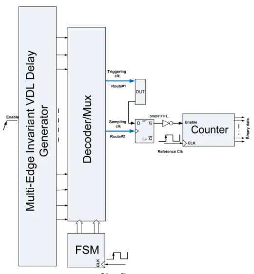
Chapter 4 describes a system architecture to measure the interconnect time delay following a triggering event. based on the Multi-Edge Invariant Vernier Delay Generator (MEIVDG), which is discussed in details in Chapter 5.
Design and circuit implementation of the proposed high resolution delay generator (MEIVDG) is discussed in Chapter 5.
Chapter 6 describes the 3D BIST techniques and applications using the proposed embedded test structures.
Chapter 7 presents TSV characterizations based on the proposed 3D BIST techniques.
Finally, Chapter 8 summarizes the dissertation and concludes by discussing about the future work involved in 3D test.
48
[Chapter 1]
Introduction to 3D Test and Technology 3D Test Challenges and Potential Solutions
3D DUT Response ExtractorsFeature Comparison
Embedded 3D Test Test Stimulus TSV Characterization [Chapter 3] Voltage Reference used for Temp
Sensors [Chapter 4] Time Delay Measurement [Chapter 5] Multi-Edge Delay Generator [Chapter 6]
On-chip Self-Test (BIST)Techniques Compatible for 3D Stacked ICs
[Chapter2]
Pass /Fall
CHAPTER 2
SIGNAL INTEGRITY AND THERMAL EFFECTS IN 3D STACKED ICS
2.1 Introduction
Three-dimensional integration is emerging as an attractive way to sustain Moore’s law, by making it possible to create highly integrated, high performance, cost effective compact structures. However, the complexity of the signal routing will grow significantly, and the high density interconnection increases the potential causes of signal integrity degradation such as crosstalk and Inter-Symbol-Interference (ISI) [26]. Moreover, high frequency signals with short distance interconnections have parasitic and transmission line effects, which may cause severe signal degradation due to reflection, distortion, and signal delays. For example; Through Silicon Vias (TSVs) can cause
Inter-Symbol-Interference (ISI) due to frequency dependent loss when data is transmitted through them, which induces severe signal integrity degradation and system faults.
On the other hand, in 3D technology, the electrical properties and system
performance depend on the materials and the geometry of the 3D structure; therefore, providing unique test techniques and methodologies for 3D designs are imperative for 3D integration. To apply 3D technology, the electrical properties of Through-Silicon-Vias (TSVs) should be characterized to estimate the quality of the signal. 3D integration will inevitably put more daunting challenges on testing future’s ICs, where conventional ATE methods appear to be more costly and unfeasible for 3D testing. This drives
researchers to adopt embedded testing methodologies, which may prove to be a very attractive solution. This embedded test approach involves building on-chip area and power efficient test IC structures on the same silicon, which normally reside around the device-under-test (DUT).
This work provides a unique method of verifying and characterizing 3D
performance by building on-chip test structures compatible for 3D IC that can provide high speed 3D I/O stimulus and testing capability. These on-chip test structures could potentially evaluate and verify the electrical models of 3D interconnects.
In this chapter, signal integrity effects and the benefit of 3D I/O characterization in 3D stacked ICs are discussed. Motivation and contribution of this work is provided. An extensive study for 3D interconnects modeling and characterization based on 3D Full wave simulator is presented. Finally, a study of the thermal effects in 3D stacked ICs is also discussed.
2.2 Signal Integrity Effects in 3D Stacked ICs 2.2.1 Introduction to Common Signal Integrity Effects
Signal integrity is a great concern in high speed designs when high clock
frequencies and higher transmission data rates are needed. Common signal integrity effects due to interconnect parasitics, which impacts system reliability, are be briefly discussed here:
Transmission Line Effect and Reflection Noise. Transmission line is the term
that is commonly used for today’s long interconnects. An interconnect can be
considered as a lumped element or a distributed RLGC model depending on its physical length’s relation to the wavelength (frequency) of the signal that it is carrying. As a rule of thumb, if the physical length of an interconnect is larger than one-tenth of the
wavelength of the signal in the line, it should be considered as a distributed
transmission line. When interconnect response is treated through distributed RLGC models, the voltage along the length of interconnect is not constant but is position and time dependent. The signal takes a finite time to travel across this interconnect and gets
![Figure 1-7. Improvement in path delay achieved using 3D technology vs. technology scaling alone [15]](https://thumb-us.123doks.com/thumbv2/123dok_us/703923.2587169/27.918.258.667.651.900/figure-improvement-delay-achieved-using-technology-technology-scaling.webp)
![Figure 1-16. Thickness stack for three-tier structure with actual layer thicknesses [22]](https://thumb-us.123doks.com/thumbv2/123dok_us/703923.2587169/38.918.174.754.113.898/figure-thickness-stack-tier-structure-actual-layer-thicknesses.webp)


![1 (4 {[(E) 5 Chloro 2 hydroxybenzylidene]amino}phenyl)ethanone oxime](data:image/gif;base64,R0lGODlhAQABAIAAAP///wAAACH5BAEAAAAALAAAAAABAAEAAAICRAEAOw==)